International Research Journal of Engineering and Technology (IRJET)
e-ISSN: 2395-0056
Volume: 06 Issue: 04 | Apr 2019
p-ISSN: 2395-0072
www.irjet.net
Analysis of Proposed FinFET Based Full Adder using CMOS Logic Style Harshita Gehlot1, Mohd Ejaz Aslam Lodhi2 1M.
Tech. Scholar, Department of ECE, Indira Gandhi Delhi Technical University for Women, Delhi, India Professor, Department of E ECE, Indira Gandhi Delhi Technical University for Women, Delhi, India ------------------------------------------------------------------------***------------------------------------------------------------------------2Assistant
Abstract - With the innovation in technology, FinFETs are
Nanometer Technologies and simulations were done at 45nm, 32nm technologies. [4]
the new emerging transistors that can work in the nanometer range to overcome Short Channel Effects (SCE) as conventional CMOS has Short Channel Effects. The logic styles used for implementation are Gate Diffusion Input (GDI) and Static Energy Recovery Full (SERF) Adder. To improve the Full Adder architecture many improvements has been made. Hence, in order to reduce the Short Channel Effects, FinFET based Full Adder has proposed. The experiment designs are implemented in CADENCE VIRTUOSO software using 180nm technology GPDK tool kit and performance analyses were done with respect to Power, Delay and Power Delay Product (PDP). Here FinFET Based GDI Adder and FinFET Based SERF Adder results in less switching activity and area due to less number of transistors i.e. 10. The result shows that the power of FinFET SERF Adder is reduced to 58.86 % compared to FinFET GDI Full Adder. The Delay of FinFET SERF Adder is reduced to 24.98% compared to FinFET GDI Full Adder. The PDP of FinFET SERF Adder has reduced to 69.14% compared to FinFET GDI Full Adder. It is evident that the FinFET based SERF Adder using CMOS Logic Style helpful in digital application in respect of portable, reliable, energy efficient, consume low power and perform high speed.
Binary addition is the basic operation found in most arithmetic components. Computation needs to be achieved by using area efficient circuits operating at high speed with low power consumption. Addition is the fundamental arithmetic operation and most fundamental arithmetic component of the processor is adder. A full adder is a logical circuit that performs an addition operation on three one-bit binary numbers. Complementary Metal-OxideSemiconductor (CMOS) is a technology for constructing integrated circuits. To improve the Full Adder architecture many improvements has been made by researchers. Full adders are fundamental cell in various circuits which is used to perform arithmetic operations and the VLSI design can be addressed at various design levels. Conventional CMOS has Short Channel Effects and difficult in implementation, thereby market demand retarding day by day. Hence, in order to reduce the Short Channel Effects, FinFET based Full Adder using CMOS logic style has been proposed. In this study, The logic styles used for implementation are Gate Diffusion Input (GDI) and Static Energy Recovery Full (SERF) Adder. The experiment designs are implemented in CADENCE VIRTUOSO software using 180nm technology GPDK tool kit and performance analyses were done with respect to Power, Delay and Power Delay Product (PDP).
Key Words: FinFET, Full Adder, GDI, SERF 1. INTRODUCTION Now a day, modern digital devices are of a great demand in many industrial applications because these devices are portable, reliable, energy efficient, consume low power and perform high speed. The most important feature of modern electronics is low power and energy efficient active block that enables the implementation of long lasting battery operated devices.
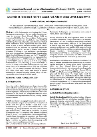
2. CMOS LOGIC STYLES 2.1 Gate Diffusion Input Operation Gate Diffusion Input (GDI) is nothing but Gate Diffusion
Input Technique. This type of technique is suitable for lower delay and designing a circuit with reduced power. This is because the technique helps to decrease the transistor count when compared with CMOS and other obtainable low power methods. [1]
FinFETs are the new emerging transistors that can work in the nanometer range to overcome these Short Channel Effects and low power FinFET based Full Adder implemented by using CADENCE VIRTUOSO tools in 45nm technology [1]. Study of different full adder cells with two logic styles i.e. FinFET Based one bit Full Adder Cell using Transmission Gate (TG) and CMOS Logic Styles At 10, 22 and 32nm[2]. Moore’s Law: Gordon Moore: co-founder of Intel. Predicted that the number of transistors per chip would grow exponentially [3]. He has set the pace for our modern digital revolution and utilized that the computing world increases in power and decreases in cost. Ultra Low Power Based one bit Full Adder using different
Š 2019, IRJET
|
Impact Factor value: 7.211
Fig-1: Basic GDI Cell [Ref 1]
|
ISO 9001:2008 Certified Journal
|
Page 4085