International Research Journal of Engineering and Technology (IRJET)
e-ISSN: 2395-0056
Volume: 06 Issue: 04 | Apr 2019
p-ISSN: 2395-0072
www.irjet.net
Simulation of High k dielectric MOS with Hfo2 as a gate dielectric Kajal Yadav1, Shivani Saxena2 1Student
of M .Tech (VLSI Design), Department of Electronics, Banasthali Vidyapith, Rajasthan, India Professor, Department of Electronics, Banasthali Vidyapith, Rajasthan, India
2Assistant
---------------------------------------------------------------------***-------------------------------------------------------------------
Abstract- Conventional MOS over 40years has been
fabricated using Silicon substrate with polysilicon in gate material. As scaling of SiO2 increases, a serious issue in terms of tunneling current and oxide breakdown raises. To overcome of these problems, silicon based MOS with High-k dielectric material in gate is becoming a strong alternative for replacing the conventional SiO2 dielectrics gates MOSFETs. High-k oxides provide a solution to leakage problems and improve performance such types of MOS can be used in both application of high performance and low power consumption. In this paper, HFO2 based high k dielectric gate is used for the formation of device because HFO2 is having high dielectric constant value and improves the performance of the device. On the basis of some electrical parameters, a comparative study in between conventional MOS and High k dielectric MOS is also presented.
Keywords: High k material, Hfo2, Leakage current, power consumption, output resistance, gate oxide.
1. Introduction: The National Technology Roadmap of semiconductor (NTRS) and ITRS having scaling predication from 100 components per IC in 1965 to 15 billion in the current state. There are less gain in device performance i.e. power Consumption, short channel effects and parasitic capacitance as scaling goes further below sub-100 nm. In 2007, the use of high-k dielectrics [6] is first time introduced, to show gate leakage issues. High K dielectric devices have applications in low power dissipation, low leakage current and high performance over conventional MOS. Basic difference in structure of conventional MOS over high k dielectric device is gate material. The materials used for the conventional MOS is SiO2 but in high K dielectric based device gate material can be HFO2, Al2O3, Y2O3, La2O3, Sc2O3 [7]. For further downward scaling, dielectric having a higher dielectric constant will be the solution for achieving the same transistor performance while maintaining a relatively thick physical thickness [6].
Š 2019, IRJET
|
Impact Factor value: 7.211
|
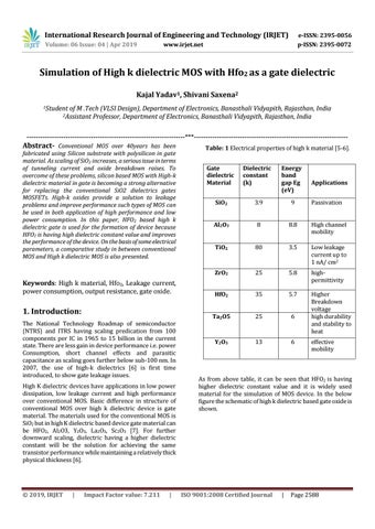
Table: 1 Electrical properties of high k material [5-6]. Gate dielectric Material
Dielectric constant (k)
Energy band gap Eg (eV)
Applications
SiO2
3.9
9
Passivation
Al2O3
8
8.8
High channel mobility
TiO2
80
3.5
Low leakage current up to 1 nA/ cm2
ZrO2
25
5.8
highpermittivity
HfO2
35
5.7
Ta2O5
25
6
Higher Breakdown voltage high durability and stability to heat
Y2O3
13
6
effective mobility
As from above table, it can be seen that HFO2 is having higher dielectric constant value and it is widely used material for the simulation of MOS device. In the below figure the schematic of high k dielectric based gate oxide is shown.
ISO 9001:2008 Certified Journal
|
Page 2588