International Research Journal of Engineering and Technology (IRJET)
e-ISSN: 2395-0056
Volume: 06 Issue: 03 | Mar 2019
p-ISSN: 2395-0072
www.irjet.net
Where is a transient (time) response, L is a load capacitance (charging or discharging), Vdd equal voltage, f equal frequency.
c
4. Simulation Results
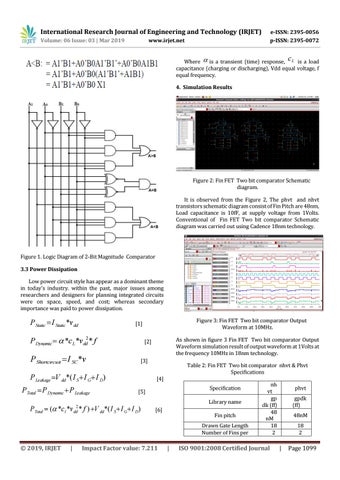
Figure 2: Fin FET Two bit comparator Schematic diagram. It is observed from the Figure 2, The phvt and nhvt transistors schematic diagram consist of Fin Pitch are 48nm, Load capacitance is 10fF, at supply voltage from 1Volts. Conventional of Fin FET Two bit comparator Schematic diagram was carried out using Cadence 18nm technology.
Figure 1. Logic Diagram of 2-Bit Magnitude Comparator 3.3 Power Dissipation Low power circuit style has appear as a dominant theme in today’s industry. within the past, major issues among researchers and designers for planning integrated circuits were on space, speed, and cost; whereas secondary importance was paid to power dissipation.
P Static I Static *v dd
Figure 3: Fin FET Two bit comparator Output Waveform at 10MHz.
[1]
P Dynamic *c L *vdd2 * f
P Shortcircu it I SC*v
[3]
P Leakage V dd*( I S I G I D) PTotal P Dynamic P Leakage
Table 2: Fin FET Two bit comparator nhvt & Phvt Specifications
[4]
Specification
[5]
PTotal ( *c l *v * f ) V dd*( I S I G I D) 2 dd
As shown in figure 3 Fin FET Two bit comparator Output Waveform simulation result of output waveform at 1Volts at the frequency 10MHz in 18nm technology.
[2]
Library name [6]
Fin pitch Drawn Gate Length Number of Fins per
© 2019, IRJET
|
Impact Factor value: 7.211
|
nh vt gp dk (ff) 48 nM 18 2
ISO 9001:2008 Certified Journal
phvt gpdk (ff) 48nM 18 2
|
Page 1099