International Research Journal of Engineering and Technology (IRJET)
e-ISSN: 2395-0056
Volume: 06 Issue: 03 | Mar 2019
p-ISSN: 2395-0072
www.irjet.net
DEISGN OF LOW POWER 16x16 SRAM WITH ADIABATIC LOGIC M. Kiran Kumar1, Amrita Sajja2, Saurabh Barpute3 ,Y. Nikhil 4, D.Yaswanth Lal5 1,2Assistant
Professor, Dept. of ECE Anurag Group Of Institutions,Hyderabad scholar & Anurag Group Of Institutions, Hyderabad -----------------------------------------------------------------------***-------------------------------------------------------------------3,4,5Research
Abstract - A SRAM or Static Random Access Memory is a
Cadence tool is used to design the SRAM cell which includes a 180nm CMOS technology, which is a standard base for the fabrication given directly to the fabrication unit.
type of semiconductor memory that uses bi-stable latching circuitry to store each bit. SRAM exhibits data remains, but it is still volatile in the conventional sense that data is eventually lost when the memory is not powered. SRAM is useful building blocks in many applications such as a data storage, embedded applications, cache memories, microprocessors. In microprocessors, large SRAM arrays are widely used as cache memory and application-specific integrated circuits can occupy a significant portion of the die area. SRAM arrays are high density circuits which are projected to occupy more than 90% of the SoC (System on Chip) area in the next 10 years. The performance of such chips is to optimized for which large arrays of fast SRAM are useful to boost of the performance. Besides, the impact of integrating large SRAM cells onto a chip will certainly lead to a higher chip cost, resulting in the involvement of millions of small size SRAM arrays are together integrated forming the densest circuitry on the chip. Access time, speed, and power consumption are the three key parameters of an SRAM memory design. In this paper an effort is made to design a low power consuming 16X16 SRAM memory array comprising of Adiabatic logic on 180nm CMOS technology using Cadence tool.
The design of a low power SRAM includes the functioning of some internally connected circuits such as Row and Column Decoders, Sense Amplifiers, SRAM Cells and Pre-Charge circuit. This paper illustrates the successful outputs of read and write operations consuming proposed low power and proper Adiabatic logic.
2. ADIABATIC LOGIC Adiabatic Logic is the term given to low-power electronic circuits that implement the reversible logic. The term comes from the fact that an adiabatic process is one in which the total heat or energy in the system remains constant. Research in this area has mainly been fueled by the fact that as circuits get smaller and faster, their energy dissipation greatly increases, a problem that adiabatic circuits promises to solve. Most research has focused on building adiabatic logic out of CMOS. However, current CMOS technology, though fairly energy efficient compared to similar technologies, dissipate energy as heat, mostly when switching. In order to solve this problem, there are two fundamental rules CMOS adiabatic circuits must follow, the reasons for which are explained below. The first is never to turn on a transistor when there is a voltage difference between the drain and source. The second says never to turn off a transistor that has current flowing through it..
Key Words: SRAM, Adiabatic logic, SOC, power consumption
1.INTRODUCTION With the rapid growth of modern communications and signal processing systems, handheld wireless computers and consumer electronics are becoming highly popular. The design of 6T SRAM has become a challenge for storage purpose in System on Chip (SoC) using Nanometer technology because of variations in the threshold values. The read/write operations carried out in the SRAM and the stability of the SRAM are effected due to the threshold variations. The SRAM is major component only occupies a larger area of the chip die. The demand for static randomaccess memory (SRAM) is increasing with large use of SRAM in mobile products, System On-Chip (SoC) and high performance VLSI circuits. SRAM covers an area of about 70% of the System on Chip. SRAM is a crucial component which has embedded use such as many scientific and industrial subsystems, automotive electronics and can be used as a cache memory in CPUs, microcontrollers, external burst mode SRAM caches and handheld devices.
Š 2019, IRJET
|
Impact Factor value: 7.211
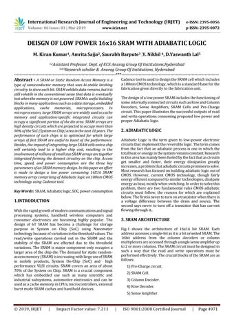
3. SRAM ARCHITECTURE Fig-1 shows the architecture of 16x16 bit SRAM. Each address accesses a single-bit as it is a bit oriented SRAM. The 16bit address from the column decoders or column multiplexers are accessed through a single sense amplifier up to 2 or more columns. The SRAM circuit must be designed in such a way that the read and write operations must be performed effectively. The crucial blocks of the SRAM are as follows: 1) Pre-Charge circuit. 2) SRAM Cell. 3) Column Decoder. 4) Row Decoder. 5) Sense Amplifier
|
ISO 9001:2008 Certified Journal
|
Page 4971