International Research Journal of Engineering and Technology (IRJET)
e-ISSN: 2395-0056
Volume: 06 Issue: 12 | Dec 2019
p-ISSN: 2395-0072
www.irjet.net
A Survey approach: Device for Biosensing Application Shradhya Singh1, Krishnakant Chaubey2, Nandini Kumari3 1,2Assistant
Professor, Dept of Electrical and Electronics Engineering Professor, Dept of Civil Engineering 1,2,3Lok Nayak Jai Prakash Institute of Technology, Chapra, Bihar ---------------------------------------------------------------------***---------------------------------------------------------------------3Assistant
Abstract - Field-effect transistors have emerged in the field of biosensors over the last few years, due to their attractive simplicity and high sensitivity to interfacial changes, both on the gate and Si body interface, where a target-specific bio receptor can be immobilized, which can be treated as a cavity. This article reviews the recent literature concerning biosensing with such type of field effect transistors, gives clues to understanding the basic principles under which field-effect transistors work, and details the transduction mechanisms that were investigated to convert a receptor/target association into a change in threshold voltage, which is treated as biosensing metric. Key Words: modulation
Junctionless, biomolecules, dielectric
1. INTRODUCTION Biosensor has been defined by the International Union of Pure and Applied Chemistry (IUPAC), is that “a device which uses specific biochemical reactions mediated by isolated enzymes, immune systems, tissues, organelles or whole cells to detect chemical or biological compounds, usually by use of electrical, thermal or optical signals” [1,2]. Biosensors are capable analytical tools for monitoring food toxins and pathogens, and environmental screening due to their unique characteristics of affordability, portability, disposability, and simple construction [3]. Biosensors are not able to just sense basic parameters such as humidity or pH, but also numerous types of non-biological compounds such as heavy metals or small organic pollutant molecules such as bisphenol A. However till now biosensors are not spread out in the market So transistor can be a great alternative to interface the biomolecule with it for sensing application.
[6], reported Junction Less Transistor, having lower Drain Induced Barrier Lowering and enhanced on-state and transfer characteristics than that of the usual MOSFETs [7], [8]. Therefore, junctionless transistors are widely used for biosensing application. 2. Biosensors with FETs The use of the concept of dielectric modulation of a vertical nanogap in the FET’s gate due to the presence of biomolecules has enabled the application of FET biosensors for detecting the presence of charge-free biomolecules as well [9-10]. The reported dielectric-modulated FET (DMFET) based biosensors show high responsiveness to both dielectric modulation and charge of the biomolecules, with the two effects often affecting the device parameters in opposite directions leading to reduced sensitivity [11]. The proposed structure demonstrates high sensitivity for biomolecule detection and retains dielectric-modulation as the dominant effect, as opposed to the conventional DMFETs where the impact of biomolecule charges on the device sensitivity is significant. The proposed sensor device shows good scalability across process technology nodes and can be an exciting alternative to FET biosensors for both advanced technology nodes as well as the older technology nodes where low-cost is the driving factor.
Nowadays, the most popular transistor used is the fieldeffect transistor (FET) [4], past research study shows that field-effect transistors have been highly appreciated for biosensing applications, because of their nano level scaling make the sensing device portable and also because the field effect is capacitance-related, and this capacitance shows high sensitivity towards surface changes, as it effects the overall characteristic of the transistor. It is very difficult to create ultra sharp doping profile between source/drain (S/D) regions with body region at nanoscale level. Several novel MOSFET designs have been developed to defeat the fabrication issue. Colinge et. al. [5] © 2019, IRJET
|
Impact Factor value: 7.34
|
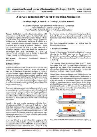
Fig.1 cross sectional view of device of reference paper [12]
ISO 9001:2008 Certified Journal
|
Page 2865