International Research Journal of Engineering and Technology (IRJET)
e-ISSN: 2395-0056
Volume: 04 Issue: 07 | July -2017
p-ISSN: 2395-0072
www.irjet.net
Characterization of 6T CMOS SRAM in 65nm and 120nm Technology using Low power Techniques Sumit Kumar Srivastavar1, Er.Amit Kumar2 1
Electronics Engineering Department, Institute of Engineering & Technology, Dr.A.P.J. Abdul Kalam Technical University, Lucknow-226021, U.P, India 2 Assistant Professor, Electronics Engineering Department, Institute of Engineering & Technology, Dr.A.P.J. Abdul Kalam Technical University, Lucknow-226021, U.P, India ---------------------------------------------------------------------***---------------------------------------------------------------------
Abstract - As the channel length of MOSFETs is scaling
maximum supply voltage (e.g. Vd = 0.7V) and the minimum ground level voltage (Vs = 0V) to them through switches that are turned on. So the SRAM circuit can operate quickly. On the other hand when the SRAM circuit are in stand-by mode, it generates slightly lower supply voltage and relatively higher ground level voltage. The present work describes such an analysis and shows that use of SVL switch for reducing supply voltage yields the maximum reduction in leakage currents especially when the pre charge. Transistors are put in cut-off state during the stand-by mode. An SVL switch can be used either to reduce the supply voltage to the SRAM cell or increase the potential of ground level and the two approaches can be combined as well. Although a technique similar to use of SVL for raising the ground potential has already been reported to yield significant reduction in gate leakage currents [5],
down, the Power dissipation of the SRAM cells become the major concern for future technology. In this paper, stable SRAM cell’s power dissipation reduction in 6T static random access memory (SRAM), is described by using dynamic self- controllable voltage level (SVL) switch. Total power dissipation is reduced by 74/% and 84% at 1.2 volt and die area is increased by 36% and 69% from 120nm to 65nm technology respectively. The schematic and layout are drawn on 120nm and 65nm technology file on a Dsch tool and their analysis is done on a Microwind 3.1 tool and BSIM simulator. Key Words: Static Random Access Memory (SRAM), 6T memory cell, area, power dissipation, 120nm65nm. SRAM , Stand-by power.
1. INTRODUCTION Design techniques for low-power circuits, for example, for use in battery-driven mobile phones, are not only storage circuits (such as flip-flops, register files, and memories) but also needed for logic circuits (such as very fast adders and multipliers). An integrated static random access memory (SRAM) is proposed to reduce leakage power at circuit and architectural level [1]. There are several techniques for reducing standby power. One of the method is multi threshold-voltage CMOS (MTCMOS). This technique reduces the power supply through the use of nMOSFET switches with higher threshold Vthn voltage and pMOSFET switches with higher threshold voltage Vthp. However, it has serious drawbacks such as the need for additional fabrication processes for higher Vthp and higher Vthn and the fact that storage circuits based on this technique cannot retain data. To solve this drawback, a self-contollable voltage level switch, which can decrease stand-by power, while maintain the high speed performance [2]. There is a significant increase in the subthreshold leakage due to its exponential relation to the threshold voltage, and gate leakage due to the reducing gate-oxide thickness [3]. The subthreshold leakage current is exponentially dependent on the gate-to-source voltage of a MOSFET [4]. When the SRAM circuit are in active mode, the SVL switch generated
Š 2017, IRJET
|
Impact Factor value: 5.181
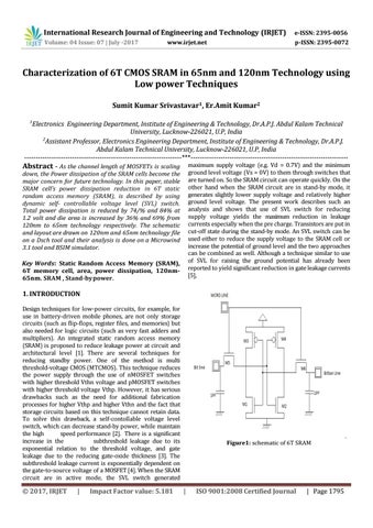
Figure1: schematic of 6T SRAM
|
ISO 9001:2008 Certified Journal
| Page 1795
.