International Research Journal of Engineering and Technology (IRJET) Volume: 04 Issue: 05 | May -2017
e-ISSN: 2395 -0056
www.irjet.net
p-ISSN: 2395-0072
MATHEMATICAL MODELLING AND PERFORMANCE ANALYSIS OF HIGH BOOST CONVERTER WITH COUPLED INDUCTOR Praveen Sharma (1), Bhoopendra Singh(2), Irfan Khan(3), Neha Verma(4) (1), (2), (3), Electrical
Engineering Department University Institute of Technology, RGPV Bhopal India (4) Medi-Caps University Indore India --------------------------------------------------------------------------***---------------------------------------------------------------------
Abstract- In this work, High boost converter is analyzed
mathematically modeled, designed with given parameters. This paper explains the mathematical modeling of high boost converter for continuous and discontinuous mode of operation for low power application. Input to the high boost converter is the unregulated supply which is obtained by rectifying AC supply. In the proposed model, DC battery fictitiously represents the unregulated supply.
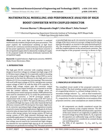
a cascaded high step-up dc–dc converter to increase the output voltage of the micro source to a proper voltage level for the dc interface through dc–ac inverter to the main electricity grid [910]. The proposed converter is a quadratic boost converter with the coupled inductor in the second boost converter. The circuit diagram of the proposed converter is shown in Fig.1 D
3
Keywords: Coupled Inductor, High boost converter, MOSFET, Diode, Power Electronics, Filter.
o2
D
1
1
N
R
D
2
4
V
DC
The high gain DC-DC converter with coupling inductor is design to boost low voltages to voltages into high range of 30 to 50 times input voltage [1]. It is especially useful in boosting low solar panel voltage to high voltage, so that 230V ac can be generated. At the time the efficiency is also high and it is cost effective [2-3]. It is a transformer less topology. This converter will work with input voltage of 25V dc, and generate constant output voltage of 440 V dc with the help of PI controller. To achieve high voltage output, gain the converter output terminal and boost output terminal are connected in serially with the isolated inductor with less voltage stress on controlled power switch and power diodes. PSIM software has been used for simulation [4-5]. To verify the performance of the proposed converter, a 345-W prototype sample is implemented with an input voltage range of 20–40 V and an output voltage of up to 440 V. The upmost efficiency of 93.3% is reached with high-line input; on the other hand, the full-load efficiency remains at 89.3% during low-line input. High boost dc-dc converter operating at high voltage regulation is mainly required in many industrial applications. High gain dc-dc boost converter play an important role in renewable energy sources such as solar energy system, fuel energy system, DC back up energy system of UPS, High intensity discharge lamp and automobile applications. For battery-powered systems, electric vehicles, fuel cell systems, and photovoltaic systems, where low-voltage sources need to be converted into high voltages, the demand for non-isolated high step-up dc–dc conversion techniques are gradually increasing [7-8]. This paper presents
|
in
N
1. INTRODUCTION
© 2017, IRJET
L
C
Impact Factor value: 5.181
|
D
2
C
1
C
o1
S1
Fig.1: High boost converter topology
2. PRINCIPLE OF OPERATION The simplified circuit model of the proposed converter is shown in Fig.2. The dual-winding coupled inductor consisted of a magnetizing inductor , primary leakage inductor , secondary leakage inductor , and an ideal transformer, which constituted the primary and secondary windings, and , respectively. In order to simplify the circuit analysis of the proposed converter, some assumptions are stated as follows. All components are ideally considered except the leakage inductor of the coupled inductor. The ONstate resistance RDS (ON) and all parasitic capacitors of the main switch S1 are neglected; in addition, the forward voltage drop of the diodes – is ignored. All capacitors are sufficiently large, and the voltages across capacitors are considered as constant during one switching period. The ESRs of all capacitors , , and are neglected.
ISO 9001:2008 Certified Journal
|
Page 1223