International Research Journal of Engineering and Technology (IRJET) Volume: 03 Issue: 09 | Sep-2016
e-ISSN: 2395 -0056
www.irjet.net
p-ISSN: 2395-0072
DEFECT DETECTION IN PCB USING K-MEAN CLUSTERING AND NEUTROSCOPY Gagandeep Kaur1, Rupinder Kaur 2 1
Gagandeep Kaur Research Scholar
Department of Computer Science And Engineering RIMT University, Fatehgarh Sahib, Punjab, india
Rupinder Kaur Assitant Professor 2
Department of Computer Science And Engineering RIMT University, Fatehgarh Sahib, Punjab, india
---------------------------------------------------------------------***--------------------------------------------------------------------with accuracy. In this we use image subtraction operation Abstract- Printed circuit board (PCB) mechanically supports .Image subtraction operation two images are subtracted to find difference between these two by pixel [10].
various components and electrically connects these components using tracks. The main goal of our work is to Detect the no. of defects in the PCB image and area of defects .The location of electronic parts is fixed and inspection time reduced. These defects are divided into two categories potential and fatal defects.Defects in PCB are in the form like missing hole, breaking lines, wrong hole size etc. During manufacturing Some defects occur in the PCB tio find these defect ,we use two techniques.These techniques are:1.Neutroscopy 2.K-mean Clustering. This paper proposes a PCB defect detection and classification system.
2. K-mean Clustering:-K-mean clustering generates a specific no. of disjoint, flat clusters. It is well suited to generating globular clusters. The k means method numerical unsupervised and non deterministic and iterative [14]. Kmean clustering is using the image subtraction operation to find the difference between the reference and test image.
Key words— PCB; Defect detection; Subtraction Operation; Neutroscopy; K-mean Clustering.
1. INTRODUCTION Printed circuit board connects electronic components together with the help of tracks [1]. During the manufacturing process of PCB various defect are caused which make our PCB unsuitable for use [5][6] . To make them usable first we have to find these detects [1]. These detect are in the form of like missing hole, breaking lines, wrong hole size etc. are PCB defect detection has great impact on the PCB manufacturing caused by the defected PCB [7]. In order to minimize these defect caused by the wrongly etched PCB panel various techniques are used [3]. The techniques used for detection are as:
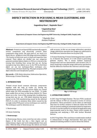
Fig -1: PCB Image
2. LITERATURE SURVEY In 2011 Ajay Pal Singh Chauhan- The bare PCB is analyzed and the defects of PCB are extracted in terms of various parameters. These parameters can be taken as referential data base for further analysis to fabricate defect free PCB and can assist in making an automated system for inspection. In order to use this method in an industrial application some improvements need to be done. Future work consists of inspecting and analyzing a PCB with Surface Mounted Devices.
1. Neutroscopy 2.K-mean clustering 1. Neutroscopy:
In 2013 Yang Halin- This used linear transformation method in enhancement of image characteristic then gray scale statistical matching method is used to detect the defects.
In Neutroscopy theory, every event has not only a certain degree of the truth, but also a false degree and an indeterminacy degree and work independently from each other. With the help of Neutroscopy the defects are found
Š 2016, IRJET
|
Impact Factor value: 4.45
|
ISO 9001:2008 Certified Journal
|
Page 314