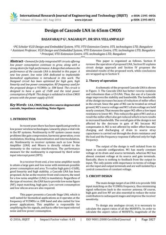
International Research Journal of Engineering and Technology (IRJET)
e-ISSN: 2395 -0056
Volume: 03 Issue: 08 | Aug-2016
p-ISSN: 2395-0072
www.irjet.net
Design of Cascode LNA in 65nm CMOS BASAVARAJ P G1, NAGARAJ P2, DR SIVA YELLAMPALLI3 1PG Scholar VLSI Design and Embedded System, VTU, VTU Extension Centre, UTL technologies LTD, Bangalore Assistant Professor, VLSI Design and Embedded System, VTU Extension Centre, UTL technologies LTD, Bangalore 3 Principal, VTU Extension Centre, UTL technologies LTD, Bangalore ---------------------------------------------------------------------***--------------------------------------------------------------------2
Abstract - Demand for fully-integrated RF circuits offering
This paper is organized as follows. Section II reviews the operation of proposed LNA, Section III explains circuit design approach and Section IV proposes the simulated results of the proposed work, while conclusions are wrapped up in Section V.
low power consumption continues to grow, along with a strong desire for high performance. A design that enhances the performance of the cascode LNA is detailed in this paper. A new low power, low noise LNA dedicated to implantable biomedical applications is introduced in this work. The Designed circuit has been optimized for high gain, high linearity and low power consumption. RF frequency used for the proposed design is 915MHz i.e. ISM band. The circuit is designed to have a gain of 15dB and the total power consumption of 49µW. This design is validated in 65nm CMOS process with the power supply of 0.6V.
2. Theory of operation A schematic of the proposed Cascode LNA is shown in Figure. 3. The Cascode LNA has better reverse isolation and robustness than a CS-LNA. Thus, the use of a Cascode stage improves the stability and bandwidth. The bandwidth of the design increases because of reduction of miller effect in the circuit. Since the gate of M2 can be treated as virtual ground, M2’s source voltage and M1’s drain voltage are held nearly constant. That means the upper M2 offers a low input resistance to lower M1. This reduces the gain of M1 and as a result the miller effect also get reduced which in turn results in increased bandwidth. The overall gain of the design is not affected by the decrease in gain of M1 because M2 compensates it. M2 is not affected by miller effect because charging and discharging of drain to source stray capacitance is carried out through the drain resistance and the load and the frequency response if affected only for high frequency.
Key Words: LNA, CMOS, Inductive source degenerated cascode, Impedance matching, Noise figure.
1. INTRODUCTION In recent years there has been significant growth in low power wireless technologies. Linearity plays a vital role in the RF systems. Nonlinearity in RF system causes many problems like gain compression, harmonic generation, cross modulation, blocking, desensitization and intermodulation, etc. Nonlinearity in receiver systems such as Low Noise Amplifier (LNA) and Mixers is directly related to the immunity to the various interferences. The performance measure for the nonlinearity is expressed by third order input intercept point (IIP3).
The output of the design is well isolated from its input in cascode configuration. M1 has nearly constant voltage at its drain and source terminals, whereas M2 has almost constant voltage at its source and gate terminals. Basically, there is nothing to feedback from the output to input. The only points with importance in-terms of voltage are the input and output terminals and are well isolated by a central connection of constant voltage.
In a receiver front-end, a low noise amplifier needs to attain a large gain and low noise with minimum possible power consumption and area. To realize high gain (>15dB), good linearity and high stability, a Cascode LNA has been proposed. As far as the receiver front-end concern, the need for a low noise amplifier (LNA) is mandatory. Regardless of the type of receiver, the LNA has to provide low noise figure (NF), input matching, high gain. Low current consumption and low silicon area are also required.
3. CIRCUIT DESIGN The main design target of an LNA is to provide 50Ω input matching on the 915MHz frequency, thus minimizing signal reflections back to the receiver antenna. Of course, high gain and low NF are also essential to reduce the noise contribution to subsequent stages and improve the receiver sensitivity.
This paper presents a Cascode Stage LNA, which is well suited for biomedical applications as it operates at the frequency of 915MHz i.e. ISM band and also suited for low power applications. This amplifier is responsible for amplifying the bio signals, and has to offer low input referred noise and low power consumption.
© 2016, IRJET
|
Impact Factor value: 4.45
To design any analogue circuit, it is necessary to calculate the aspect ratios of all the MOSFETs. In order to calculate the aspect ratios of MOSFETs, magnitude of the
|
ISO 9001:2008 Certified Journal
|
Page 1827