International Research Journal of Engineering and Technology (IRJET)
e-ISSN: 2395 -0056
Volume: 03 Issue: 07 | July-2016
p-ISSN: 2395-0072
www.irjet.net
Slotted UWB Antenna for Bandwidth and Gain Enhancement Mr. Murthi Mahadeva Naik G, Ms. Audre Arlene A, Dr. Naveen Kumar S K Mr. Murthi Mahadeva Naik G, Dept. of E&C, Malnad College of Engineering, Hassan, India. Ms. Audre Arlene A, Dept. of E&C, Malnad College of Engineering, Hassan, India. Dr. Naveen Kumar S K, Dept. of E&C, Mangalore University, Mangalore, India, ---------------------------------------------------------------------***--------------------------------------------------------------------filter is used to obtain desired band-notch characteristics. Fractal structure [8] and defected ground structure (DGS) [9] are other approaches used for band-notch purposes. In this letter, a novel microstrip-fed slot antenna with modified radiation patch and ground plane is suggested to provide band-notch purpose. Etching a circular slot with three arms on a radiating patch leads to improvement of bandwidth, and then by biasing one diode or both of them, single and dual band-notch function is achieved, respectively. The ground plane has also two symmetrical triangular-shaped slits to improve bandwidth and two extra rectangular slots to get better notch function. Additionally, a single rectangular slot is etched under the feedline on the ground plane to get a better impedance bandwidth according to [5] and [9]. The proposed design controls width and the position of notched frequencies. Dimensions of the designed antenna are small, and its structure has less complexity and better functionality. Additionally, novelty in comparison to previously presented antennas is another specification of this design, and with just two p-i-n diodes, three band-notch states are investigated.
Abstract - A novel written ultrawideband (UWB) slot
antenna with reconfigurable band-notch characteristics is bestowed during this letter. The projected antenna consists of a modified rectangular radiation patch with a circular and 3 rectangular-shaped slots etched thereon. in addition, by cutting 2 triangular-shaped slits on a changed ground plane, sensible halfway information measure of additional than a hundred and twentieth (3.12–12.51 GHz), outlined by ten decibel come loss, is achieved. so as to come up with single and twin band-notch characteristics, two p-i-n diodes ar mounted across the circular slot. The designed antenna has tiny size of twenty twenty millimetre with switchable single notched bands of three.12–3.84 gigacycle per second WiMAX and 5– 6.07 GHz WLAN, once diode one and diode a pair of ar severally on. Also, dual bands of 3.12–3.82 and 4.9–6.06 gigacycle per second ar eliminated from whole frequency band once each diodes ar at the same time on.
Key Words: Band-notch, microstrip slot antenna, reconfigurable, p-i-n diodes. 1. INTRODUCTION
2. ANTENNA CONFIGURATION AND DESIGN
Due to the rapid growth of ultrawideband (UWB) communication systems and their inherent properties such as ultra-wide impedance bandwidth, omnidirectional radiation pattern, constant gain, high radiation efficiency, constant group delay, low profile, and easy manufacturing [2], which distinguish them among other systems, there is an essential call for efficient communication devices to work in such environments. Among newly proposed antenna designs, slot antennas are good candidates with very high radiation efficiency, less dispersion, and easy integration of switches. Also, there are assigned frequency bands such as WLAN (5.15–5.35) and (5.725–5.825) GHz and WiMAX (3.3–3.6) GHz, which are also operated in UWB portion, so the problem of interference emerges. As a solution, several UWB antennas have been attempted to overcome the interference problem using frequency band-rejected function designs. In [4], parasitic structure in a monopole antenna with wideband to single and dual band-notch functionality is proposed. Also in [7], notch function is done by the means of parasitic patches. A slotted patch (i.e., inverted V-shaped slot with folded ends) has been designed to omit WLAN band [2]. In [6], bandstop
© 2016, IRJET |
Impact Factor value: 4.45
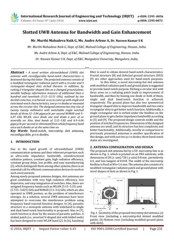
The proposed slot antenna fed by a 50- microstrip line is as shown in Fig. 1, which is printed on an FR4 substrate, with dimensions of 20 (x -axis) *20 ( y-axis) 0.8 mm , permittivity 4.4, and loss tangent of 0.018. The width of the microstrip feedline is fixed at Wn=1.6 mm. The antenna also consists of a modified rectangular radiation patch and ground plane with novel shapes of slots as shown in Fig. 1.
Fig. 1. Geometry of the proposed microstrip slot antenna. (a) Front view (including a microstrip-fed slotted modified patch). (b) Bottom view (including modified ground plane with slots).
|
ISO 9001:2008 Certified Journal
|
Page 232