Circuit Approaches for VLSI in Internet-of-Things Applications
KM Sandhya Bhashkar1 , Sushil Chandra Agrawal21M.Tech, VLSI, National Institute of electronics and information technology, U.P, India

2Principal & Technical Officer, Department of VLSI, National Institute of electronics and information technology, U.P, India
Abstract - IoT circuit designers confront problems and possibilities. Security and power management are essential for billions of devices that perceive, compute, communicate, and interact. The physically unclonable function (PUF) is becoming increasingly essential in hardware-security applications because it gives device variations an object-specific physical identity that is hard to disclose and replicate by adversaries. Creating a tiny PUF that can withstand voltage, temperature, and noise is tough. This thesis proposes PUFs with two ultrasmall analog circuits that output absolute temperature. Two works demonstrate the proposed method: (1) an ultracompact and robust PUF based on voltage-compensated proportional-to-absolute-temperature voltage generators, which takes up 8.3 less area than the previous work and twice the robustness of the most compact PUF design; and (2) a method to transform a 6T-SRAM array into a robust analog PUF with minimal overhead. This work uses a similar circuit design to convert an on-chip SRAM into a PUF, lowering size in (1) without sacrificing robustness.
When battery replacement is expensive, an Internet of Things sensor node needs energy harvesting. EH, PMUs lose efficiency during voltage transfer from harvester to battery and battery to load. A capacitor buffers energy flow in an EH PMU with hybrid energy storage.
Key Words: VLSI Design, IoT Applications, Circuit Approaches, Low Power Design, Energy Efficiency, UltraLowPower.
1. INTRODUCTION
A VLSI circuit is like a tiny electronic puzzle made up of manysmallcomponentscalledtransistors.Itisdesignedto performspecifictasksbycontrollingtheflowofelectricity. Think of it as a mini-orchestra conductor that guides the movementofelectronstocreateusefulfunctions.
Thesecircuitsaremadeofaspecialmaterialcalledsilicon, and they are so small that you need a microscope to see them.Eachtransistoractslikeaswitch,allowingorblocking theflowofelectricity.Byarrangingtheseswitchesinclever ways,wecanmakethecircuitdodifferentthings,likeadding numbers,storinginformation,orevenplayingmusic.
The VLSI circuit is all about making connections. It has pathwayscalledwiresthatconnectthetransistors,allowing them to work together as a team. The design of these
connections is crucial because it determines how well the circuitperformsitstasks.
Justlikehowapuzzleneedstobeputtogetherintheright waytowork,theVLSIcircuitneedstobecarefullydesigned and manufactured to function properly. Engineers use specialcomputerprogramstoplanandcreatethesecircuits, makingsureeverythingfitstogetherperfectly.
VLSIcircuitsareusedinallsortsofelectronicdevices,from smartphonesandcomputerstocarsandhomeappliances. Theyarethebuildingblocksofmoderntechnology,making itpossibleforourdevicestoperformcomplextasksquickly andefficiently.
Insimple terms,a VLSI circuitisa small electronic puzzle madeoftinyswitchesthatcontrolelectricity.Itisdesigned to do specific jobs and is used in many of the electronic devicesweuseeveryday.
1.1. Factor Affecting Performance of VLSI Circuit
Several factorscanaffecttheperformanceofa VLSI(Very LargeScaleIntegration)circuit.Herearesomekeyfactorsto consider:
1. ClockFrequency:Theclockfrequencydetermines thespeedatwhichthecircuitoperates.Higherclock
frequencies generally result in faster circuit performance. However, increasing the clock frequency can also lead to higher power consumptionandincreasedheatgeneration.
2. Transistor Size and Technology: The size and technologyofthetransistorsusedintheVLSIcircuit haveasignificantimpactonperformance.Smaller transistors allow for higher packing density and faster switching times, leading to improved performance. Advanced semiconductor technologies,suchasFinFETornanoscaleprocess nodes,offerbetterperformancecharacteristics.
3. InterconnectDelay:Theinterconnectsthatconnect differentcomponentsinthecircuitintroducedelay. Longerinterconnectsandhigherresistancecanlead to increased signal propagation delay, impacting overallcircuitperformance.Designtechniqueslike buffering, routing optimization, and interconnect scalinghelpmitigateinterconnectdelay.
4. Power Consumption: Power consumption affects theperformanceofVLSIcircuitsinmultipleways. Excessivepowerconsumptioncanleadtoincreased heat dissipation, reliability issues, and reduced batterylifeinportabledevices.Poweroptimization techniques,suchasvoltagescaling,clockgating,and power gating, are employed to balance power consumptionandperformance.
5. Circuit Design Techniques: Various circuit design techniquescanimpactperformance.Designchoices like pipelining, parallelism, and data path optimizationscanimprovethroughputandlatency. Additionally,efficientmemoryarchitectures,such as cache designs and memory hierarchy, play a crucialroleinperformanceoptimization.
6. Noise and Signal Integrity: Noise, including crosstalk,electromagneticinterference(EMI),and power supply noise, can degrade signal integrity andimpactcircuitperformance.Propershielding, signalisolation,andnoisereductiontechniquesare essential for maintaining signal integrity and maximizingperformance.
7. ProcessVariations:Variationsinthemanufacturing processcanimpacttheperformanceofVLSIcircuits. Process variations can lead to differences in transistorcharacteristics,interconnectresistance, and capacitance, affecting circuit speed and reliability. Design techniques like process corner optimization and statistical analysis help account forprocessvariations.
8. Temperature:Circuitperformancecanbeaffected bytemperaturevariations.Highertemperaturescan cause increased leakage currents and degraded transistorperformance,leadingtosloweroperation and potential reliability issues. Thermal management techniques, such as heat sinks and thermal design optimization, are employed to controltemperatureandmaintainperformance.
9. Design Constraints: Design constraints, including area constraints, timing constraints, and power constraints, can impact performance. Balancing theseconstraintsandoptimizingthedesignwithin these limitations is crucial for achieving desired performance.
OptimizingperformanceinVLSIcircuitsinvolvesacareful balance of these factors, considering the specific requirementsof thecircuit'sapplicationandthe available designresources.Designersstrivetoachievethebesttradeoffs between performance, power consumption, area utilization, and reliability to create efficient and highperformingVLSIcircuits.
2. FULLY-INTEGRATED POWER MANAGEMENT CIRCUITS
Inthevastrealmofelectronicenchantment,fully-integrated power management circuits emerge as the ethereal guardiansofenergyflow,gracefullyorchestratingthedance between power sources and the multitude of hungry electronicsoulstheynourish.
Thesemagicalcircuits,akintominiaturepowersorcerers, possess the ability to harness and manipulate the elusive currentsofelectricity,ensuringtheyflowharmoniouslyto eachcomponentinneed.Likeasymphonyconductor,they deftlybalancethedelicateartofpowerdistribution,granting lifetotheelectronicrealm.
Withinthedepthsoftheirintricatecircuitryliesatapestryof enchantments.Pulse-widthmodulationspellsimbuethem withthepowertocontrolenergylevels,adjustingtheflowto meet the needs of their charges. Voltage regulators, with their mystical incantations, ensure that the currents are stable and pure, protecting the delicate souls of the electronickingdom.
Thesecircuitspossessaboundlessversatility,adaptingtheir enchantments to fit the needs of diverse realms. They gracefullydancealongsideprocessors,sensors,andmemory, empoweringthemwithjustthe rightamountofenergyto thrive. Whether it be the fleeting whispers of a handheld device or the mighty roar of a high-performance system, thesecircuitsbestowtheirmagicalenergyuponall.
Fully-integratedpowermanagementcircuitsarethe evervigilant custodians of efficiency and conservation. Their

spellsofefficiencyenchant,ensuringthatnodropofenergy iswasted, and the electronic realmflourishessustainably. Energy-harvesting enchantments capture the ambient energiesoftheworld,transformingthemintopreciousfuel topowertheever-growingrealmofdevices.
Astheyweavetheirmagic,thesecircuitsalsosafeguardthe electronic kingdom from harm. Protection spells guard againstovervoltage,overcurrent,andoverheating,shielding thedelicatecomponentsfromtheravagesofelectricalchaos. Theirwatchfuleyesandlightning-quickresponsesshieldthe realmfromharm,ensuringitslongevity.
In this realm of electronic enchantment, fully-integrated powermanagementcircuitsaretheunsungheroes,working tirelessly to nourish and protect the electronic landscape. Their presence is often hidden, tucked away within the labyrinthinedepthsofdevices,yettheirinfluenceisfeltin everymomentofoperation.
Truly,thesecircuitsarethekeepersoftheelectronicflame, illuminating our lives with the magic of technology. With theirdelicatebalanceofpowerandprotection,theybreathe lifeintoourdevices,empoweringthemtoweavetheirspells ofconnectivity,computation,andcommunication.
3. Analog PUF Architecture in VLSI Circuit
AnalogPhysicalUnclonableFunction(PUF)architecturein VLSI(VeryLargeScaleIntegration)isadesignapproachthat utilizestheinherentvariationsinanalogcircuitstocreatea uniqueidentifierforeachintegratedcircuit.
Inanalogcircuits,someslightdifferencesorvariationsoccur duringthemanufacturingprocess.Thesevariationscanbe causedby factorssuchasprocessvariations,temperature fluctuations,oragingeffects.AnalogPUFarchitecturetakes advantage of these variations to create a unique response thatcanserveasadigitalfingerprintforeachchip.
The architecture of an Analog PUF typically involves a challenge-responsemechanism.Aspecificinput,knownas the challenge, is provided to the PUF. The PUF then generatesaresponsebasedontheuniquecharacteristicsof the circuit. This response is specific to the individual chip and cannot be replicated, making it suitable for authenticationorsecuritypurposes.
AnalogPUFsoffercertainadvantagesoverdigitalPUFs.They aregenerallymoreresistanttomodelingattacksandreverse engineering because the variations in analog circuits are complexanddifficulttoreproduceaccurately.Additionally, Analog PUFs can be implemented using simple circuit elements,makingthemefficientintermsofareautilization andsuitableforintegrationintoVLSIchips.
However,AnalogPUFsalsofacechallenges.Thevariations thatmakeeachPUFuniquecanintroducesomeinstabilityin
theresponseovertimeorduetoenvironmentalconditions. Tomitigatethis,calibrationandcompensationtechniques areemployedtoensurethereliableandconsistentoperation ofthePUF.
In essence, Analog PUF architecture in VLSI exploits the inherentvariationsinanalogcircuitstocreateuniqueand unclonable identifiers for individual chips. By leveraging these variations, Analog PUFs provide a reliable and unpredictableresponsethatcanbeusedforauthentication, security, and other applications where uniqueness and trustworthinessarerequired.
4. PHOTOVOLTAIC POWER HARVESTING AND POWER LOSS IN IoT NODES UNDER DIFFERENT LIGHTING CONDITIONS
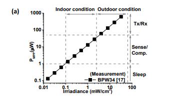
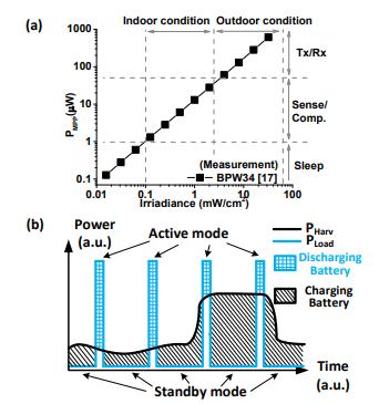
Analternatearchitecturalarrangementhasbeensuggested as a potential answer to the issue to avoid the need for a high-ratioconversion.Thishasbeendonetosolvetheissue. These two modes are known by their respective names. Despitethis,itcanoperateinseveralvariouswaysaswell. Thisissomethingthatmaybeconsideredapossibility.Inthe mode that is referred to as directly charging, it creates a connection between a PV cell and VLoad while at the same time keeping control over VLoad by storing any additional energy in the battery. This model is referred to as "direct charging."Whenthesystemisconfiguredtofunctioninthe modeknownasdischargingdirect,theloadwillgetpower from the battery through both the direct channel and the dischargeroute.

Figure-2: (a) Photovoltaic power harvesting and power loss in IoT nodes under different lighting conditions. b) End-to-end energy efficiency is lower when batteries are charged and discharged.
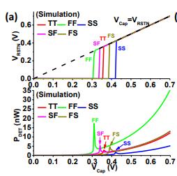
In the computations that were carried out to evaluate the trustworthinessofthecold-startstrategy,boththeCorner method and the Monte Carlo method were utilized as differentapproaches.AscanbeseeninFigure-3andFigure4,thepredeterminedthresholdofthecold-startdetection, whichisdenotedbythedesignation"Vtrip,"variesby110 mVdependingonwhichprocesscornerisbeingconsidered (a).Thepicturedemonstratesthisdifferenceveryclearly.It hasbeendiscoveredthatthepowerconsumptionoftheEH PMU,whichismeasuredintensofnanowatts,doesnothave asignificantimpactontheeffectivenessofthedevice.

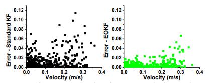
OurensembleobservationKalmanfilter(EOKF)makesuse of regression spike rates as the state observation in a KF. This results in a 400-fold reduction in the amount of processingthatisrequiredincontrasttotheconventional Kalman filter that is used for decoding (Table-1). The findings from DREAM indicate that at the higher velocity range, the performance of EOKF is superior to that of KF (Figure-5).Followingthat,thesemethodswereincludedin circuitsthatmeasured0.18micrometersinsize,hadtheir leakagedecreasedtoanideallevel,andhadbeenoptimized, respectively.ThepowerdissipationoftheNSPisatalevel that is at an all-time low of 0.61 microwatts, which is remarkable for a system that has 96 channels (6.35 nanowattsperchannel).
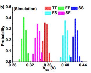
Table-1: The complexity of the calculation is cut in half thanks to EOKF.

5. CO-DESIGN OF THE PMU AND NSP FOR VLSI

PMU(PowerManagementUnit)andNSP(NoiseSuppression Unit) are two critical components in modern VLSI (Very LargeScaleIntegration)design.ThePMUisresponsiblefor regulatingthepowersupplytovariouscomponentsinthe chip,whiletheNSPisresponsibleforfilteringoutnoisefrom thepowersupply.
Co-designofthePMUandNSPisimportantbecausetheyare tightly coupled, and the design of one can affect the performance of the other. For example, the PMU must provide a stable power supply to the NSP, while the NSP mustfilteroutanynoisegeneratedbythePMU.
Oneapproachtoco-designingthePMUandNSPistousea mixed-signal design methodology. This approach involves combining analog and digital circuits to achieve optimal performance.TheanalogcircuitsareusedforthePMUand NSP, while the digital circuits are used for control and communicationbetweenthetwo.
Another approach is to use a power-aware design methodology, which takes into account the power consumptionofthePMUandNSP.Thisapproachinvolves optimizingthedesigntominimizepowerconsumptionwhile stillmeetingtheperformancerequirements.
Thehybriderror-andreplica-basedcontrolthatithasisthe firstcharacteristicthatdifferentiatesitfromotherspecies. In-situEDACintheNSPquicklyadjustsVDDwhenusedin conjunctionwithaprogrammableSC-DCthathasa63-ratio ratio.Withtheimplementationofarecentupgrade,theNSP EDACnowhasexpandedfunctionalities.Wemadeadvantage of the sparse insertion method to position the error detection latches (EDL) such that they were positioned betweenthequeuesandthesorters Theprocessofbodyswappingwasabletoaidinthecorrectionofinaccuracies thatweremadeintheindividual'srecalloftheirweight.We were able to conserve some power by just switching the memorybankbody,whichwasallthatwasrequiredofus (outof16).
The regulation of gene expression by replica- and errorbasedmechanismsisshowninfigure-6.Ifthereisaproblem withthetiming,thePMUcontrollerwillalterthephaseof theSC-DCtorestoretheoutputvoltage.Thisisdonetostop theoutputvoltagefromfallingbelowacertainthreshold.To providesufficientpowerforbodyswappingerrorcorrection, theSC-fSCDCsgothroughaperiodoffastsurgeduringthe coreclockcycle.Iftheissuesarenotresolved,thecontroller isprogrammedtolowertheSC-DCCR,whichwillincrease VDD. If the controller determines that the issues have not beenfixed,thiswilltakeplace.
6. CONCLUSIONS
TheInternetofThingsrequirespowermanagementcircuits. Energyharvestingisaviableoptionforbatteryreplacement inlow-powerIoTnodes.EarlyEHPMUsystemslostplentyof power during harvester-to-battery and battery-to-load voltagechanges. TheEHPMUwithhybridstoragedecreases energy loss from two voltage changes, which is good. We analyzedesigntradeoffsbetweenefficiencyandenhancing capacitorcapacity,load,andharvesterpowerprofiles.The recommendedarchitecturerequirestrade-offssincethetwo efficiencyoptimizationtechniquesdisagree.IoTnodes'low power needs challenge PMU designers. Such a semiconductorneedsahighPCE,100%integration,andan adaptive DVS. The system supports both. These regions requirefurtherinvestigationfortheargument.Ourcontrol systemautomaticallyfindstheSC-idealDCconfigurationand switchingfrequencytoeliminatethelossofcomponentsand increaseVDD marginandPMUPCE.ThelatestPUFartwork showsthatrobustnessandcompactnesshaveimprovedover the previous decade, but there is always potential for improvement.ButinstabilityinweakPUFslikeoursisthe main problem. PUF analysis requires chip-stored errorcorrectingcodesandbitmasks.Thus,NVMbitmasktweaks may cause fault injection attacks. Thus, architectural data limits are unclear. "Powerful" PUF architectural designs typically employ "weak" circuit topologies. Effective PUFs needresearchintothemicrovoltagegeneratorpairdesign. TheEHPMU designhasnotbeenfullytestedina realistic harvester/loadpowerconsumptionsituation.OneSCdesign may transmit power across several voltage domains, eliminating the need for many converters. PMUs and industrial equipmentloadsmustaccountfortimeclosure. Fix hold-time violations on timing arcs when the supply voltageisphasedwiththeessentialroute.

REFERENCE
[1] B. Parhami, “Computer Arithmetic: Algorithms and Hardware Designs”, 2nd edition, Oxford University Press, NewYork,2010
[2] Milos Ercegovac, Tomas Lang, "Digital Arithmetic", MorganKaufman,2004.
[3] I. Koren, Computer Arithmetic Algorithms. Englewood Cliffs,NJ,PrenticeHall,1993.
[4] R. Zimmermann, Binary Adder Architectures for CellBased VLSI and their Synthesis, PhD thesis, Swiss Federal InstituteofTechnology(ETH)Zurich,Hartung-GorreVerlag, 1998.
[5]NeilWeste,DavidHarris,"CMOSVLSIDesign:ACircuits andSystemsPerspective"PearsonEducation,2004.
[6] Jan M. Rabaey, Anantha Chandrakasan, and Borivoje Nikolic,“DigitalIntegrated.Circuits:ADesignPerspective” PearsonEducation,2003.
[7]Weinberger,J.L.Smith,“ALogicforHigh-SpeedAddition,” Nat.Bur.Stand.Circ.,591:3-12,1958.

[8] H. Ling, “High-Speed Binary Adder,” IBM Journal of ResearchandDevelopment,vol.25,no.3,pp.156-166,May 1981
[9] Harris D, “A taxonomy of parallel prefix networks”, in. Proc.37thAsilomarConf.Signals,Systems,and.Computers, Nov.2003,Vol.2,pp.2213-2217.
[10]R.P.BrentandH.T.Kung,“ARegularLayoutforParallel Adders,”IEEETrans.Computers,vol.31,no.3,pp.260-264, Mar.1982.
[11]D.Harris,"LogicalEffortofHigherValencyAdders,"in Proc.38thAsilomarConf.Signals,Systems,andComputers, vol.2,pp.1358-1362,2004.
[12] S. Mathew, M.A. Anders, B. Bloechel, T. Nguyen, R.K. Krishnamurthy,S.Borkar,“A4GHz300-mW64-bitinteger execution ALU with dual supply voltages in 90nm CMOS,” IEEEJ.SolidStateCircuits,vol.40,no.1,pp.44-51,Jan.2005.
[13] Kumashikar et al., “Sparse Tree Adder”, US Patent 20070299902A1.
[14]T.L.Lynch,E.E.Swartzlander,“ASpanningTreeCarry LookaheadAdder”,IEEETrans.Comput.,Vol.41,N°8,pp.931939,1992.
[15] V. Kantabutra, “A Recursive Carry-Lookahead/CarrySelect Hybrid Adder”, IEEE Trans. Comput., Vol.42, N°12, pp.1495-1499,1993.
[16]O.Kwon,E.Swartzlander,andK.Nowka,“Afasthybrid Carry-lookahead/Carry-select adder design”, Proc. of the 11th Great Lakes symposium on VLSI, pp.149-152, March 2001.
[17]Oklobdzija,V.G.;Zeydel,B.R.;Dao,H.;Mathew,S.;Ram Krishnamurthy; , "Energydelay estimation technique for high-performancemicroprocessorVLSIadders,"Computer
Arithmetic, 2003. Proceedings. 16th IEEE Symposium on , vol.,no.,pp.272-279,15-18June2003.
