
International Research Journal of Engineering and Technology (IRJET) e-ISSN:2395-0056
Volume: 12 Issue: 01 | Jan 2025 www.irjet.net p-ISSN:2395-0072

International Research Journal of Engineering and Technology (IRJET) e-ISSN:2395-0056
Volume: 12 Issue: 01 | Jan 2025 www.irjet.net p-ISSN:2395-0072
Divya1, Kusumanjali Deshmukh2
1Research Scholar, Department of Physics, Govt. VYT PG Autonomous College, Durg(CG), India
2Assistant Professor, Department of Physics, Govt. VYT PG Autonomous College, Durg(CG), India
Abstract:
The addition of Ni and Co in CdSe thin film have been carried out using chemical bath deposition technique on glass substrate at 80°c temperature in which selenium dioxide is the source of Se²⁻ ions and cadmium acetate is the source of Cd²⁺ions, nickel chloride and cobalt chloride used for Ni⁺ and Co⁺ ions respectively. Samples were subjected to structural characterization using XRD, optical absorption and PL study also done, were XRD reveals the cubic structure, also the dislocation density (δ), strain (ε) and crystalline size (D) are discussed. The XRD data showed that the co-doping had a significant impact on the crystalline preferred orientation. FE-SEM images show some cabbage type structure particles having uniform distribution, PL intensity decreases with doping of Ni-Co and found direct band gap with at little high range. Co-doping of CdSe thin films withNiandCo improvedtheirsolarcellefficiency.
Keywords: Nano-crystallinethinfilms,FE-SEM,XRD,Ni-Co Co-Doping
1. INTRODUCTION
In recent years, II-IV semiconductors in nanocrystalline forms have experienced an enormous development owing their interesting size dependent opticalandelectronicproperties[1].Cadmium Selenide is one from II–VI semiconductor compounds, is a promising photovoltaic material because of its high absorption coefficient near the band edge and its direct band gap whichis1.74eV[2].Therearemanytechniquestodeposit thin films like vacuum evaporation, electrode deposition, chemicalbathdeposition,CBDmethodisthemostsuitable deposition among them due to its simplicity, affordability, and ability to deposit solid solutions without the need for complicated equipment [3-7]. We have produced uniform, veryadherent,nearlystoichiometricCdSefilmswithfewer defects because to this Methode [8]. To increase qualities ofCdSeSemiconductor,ithasbeendopedwithavarietyof elements, including In, Fe, Ni, Co, Sm, and Ag [10]. It can form in cubic (zinc blende) and hexagonal (wurtzite) While the cubic is a metastable structural phase that frequently occurs at low temperatures, the hexagonal is the stable phase of CdSe [2]. In this study, pure Cadmium Selenidefilmswerepreparedbychemical bathdeposition alongwithNiandCoco-dopingatsameratios.
Glass slides with dimensions (76mm 9×26mm 9×1mm) thathadbeenchemicallycleanedanddriedinairforsome hours,areusedassubstratesforthefilm-making process. Sodium selenosulphate (Na2SeSO3), serving as a precursor for selenide ions, was utilized in this process. 1 M solution of Na2SeSO3 was created by re-fluxing equal partsof 1M sodiumsulphite(Na2SO3)and 1M selenium dioxide (SeO2) solutions in 250 ml beaker, while continuously stirring the mixture with a magnetic stirrer at90°Cfor4h.
Chemical deposition of CdSe film is carried out at room temperature. Deposition solution is prepared by taking 7 ml freshly prepared 1 M cadmium acetate (CH₃COO)₂Cd₂H₂O,7ml1MNa₂SeSO₃,10mlammoniato adjustthepHvalueand2mlofTEAin50mlbeakergently stirring the solution at room temperature for 5 min then glass substrates were vertically immersed. The substrates with CdSe coating were taken out of the bath after depositionperiodof2hat80°Ctemperature,washedwith double distilled water and dried in air. For Ni and Co doping, to above solution 2ml of 1 M NiCl₂.6H₂O and 2ml of 1M CoCl₂.6H₂O solution was added [8]. The prepared pureCdSethinfilmisorangeredcolorandNi-Coco-doped CdSethinfilmisdarkredincolor.
3.1
The cubic phases of CdSe, Ni and Co exist, JCPDS card No (00-019-019) information for CdSe, Ni and Co selenide wasusedtodeterminethesamplephase.TheXRDpattern suggests a poly-crystalline structure, all the films demonstrate three dominant peaks at 25.55°, 42.17° and 50.67° belonging to (111), (220) and (311) planes for undopedCdSeand25.51°,42.39°and50.22°areNi-CoCodoped CdSe respectively, with doping peaks increased slightly.
International Research Journal of Engineering and Technology (IRJET) e-ISSN:2395-0056
Volume: 12 Issue: 01 | Jan 2025 www.irjet.net
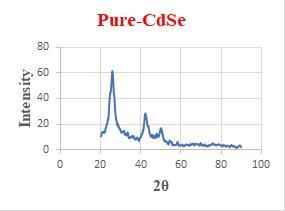
Fig:1(a)XRDgraphofPureCdSe
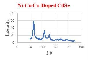
Fig.1(b)XRDgraphofNi-CoCo-dopedCdSe
The FWHM from undoped CdSe is 3.84° and when doped with Ni-Co decreased to 2.58°. Crystallite size (D) was calculatedusingDebye-Scherrerformula[16]:
D = kλ / β cosθ (1)
D of CdSe thin films was determined to be 1.65nm, while forCdSe:Ni+Cothinfilmsitwasdeterminedtobe1.68nm. Adevice'soutcomesare enhancedby goodcrystallization, confirmed by a large grain size, proving that CdSe is an excellentoptionforwindowlayer[10].
The following equation was used to calculatemicro strain (ε)[17]:
ε=βcosθ/4 (2)
The following equation was used to calculate dislocation density(��)[18]: ��=1 /
The property is nanocrystalline if the ε value is less. Polycrystallinefilms,ontheotherhand,areindicatedbya greaterε.Filmswithlowervalueswillhavehigherdegrees of crystallinity and fewer flaws. Table 1 shows the structureparameterofallfilms
Table -1: Structuralparameterofintendedfilms
The CdSe thin films in used chemical bath deposition technique the structures illustrate the first homogeneous characteristics or uniformly sized the grains on the surface,
(3)
International Research Journal of Engineering and Technology (IRJET) e-ISSN:2395-0056
Volume: 12 Issue: 01 | Jan 2025 www.irjet.net p-ISSN:2395-0072
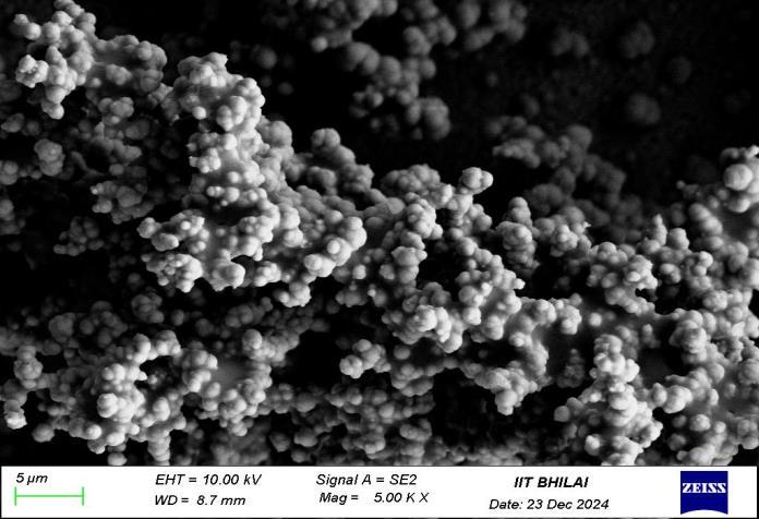
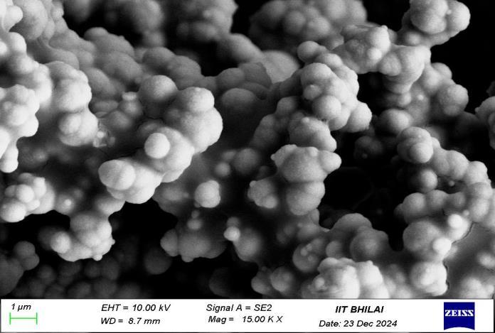
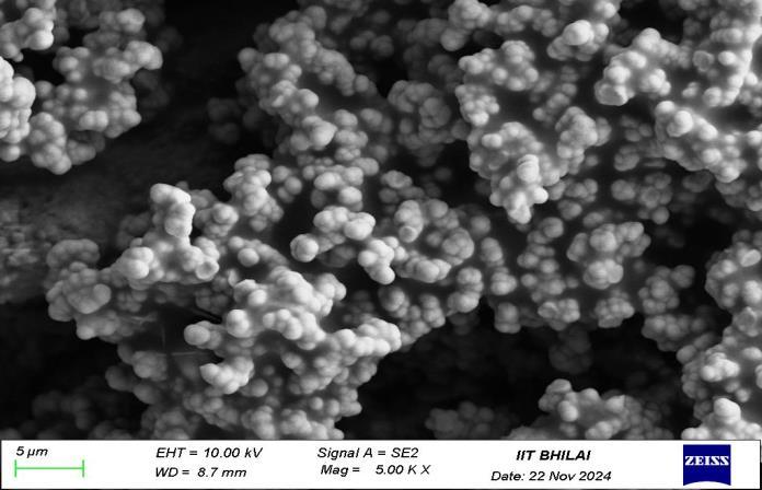
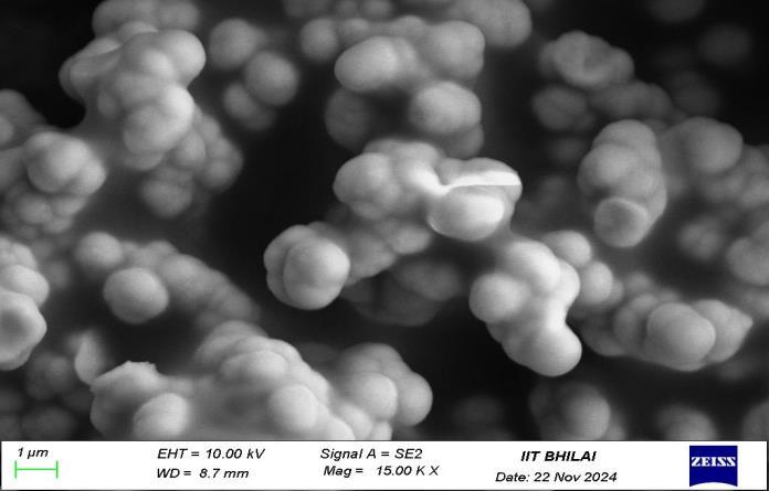
Fig:3(a)and(b)FE-SEMimageofNi-CodopedCdSe
inpresentstudyfig:2(a)and (b)showsPureCdSemanocrystallinethinfilmsurfacestructureandFig:3(a)and(b) shows Ni-Co Co-doped nano-crystalline CdSe thin films with5000and1500magnifications.FromFE-SEMimages itisclearlyvisiblethat withNiandCo-dopingtheparticle sizeisdecreases
3.3 Optical properties
Absorbance
Optical absorbance spectra were captured between 450 and750nminwavelength.ItisevidentfromFig.4(a)and (b) that co-doping raised the absorbance values as the opticalabsorbancerosewithwavelength.
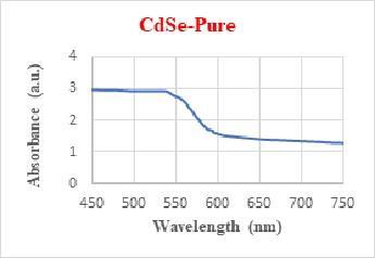
Fig:4(a)Absorbancespectraofpure-CdSe
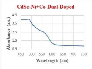
Fig.4(b)Absorbancespectraof Ni-CoCo-dopedCdSe
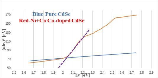
Fig:5Plotof(αhν)²vs.hν(derivedfromfig.4(a)and(b)
This could be explained by the fact that Ni and Co-doped CdSe thin films are thicker than pure CdSe films. This indicatesthat Niand Co havea greatercapacity to absorb light. Fig. 5 shows the Tauc plots for pure CdSe and Ni-Co Co-doped CdSe nanocrystalline thin films shows direct transitionanditisdirectbandgapnatureat1.94eV.
International Research Journal of Engineering and Technology (IRJET) e-ISSN:2395-0056
Volume: 12 Issue: 01 | Jan 2025 www.irjet.net p-ISSN:2395-0072
PureandNi-CodualdopedCdSethinfilmswereexamined for their structural and optical characteristics. The structural investigation verified that the cubic system is present in both pure and Ni-Co Co-doped CdSe thin films. ThecrystallitesizeandlatticepropertiesofCdSethinfilms were altered by co-doping with Ni and Co, by doping the crystallite size shrank. The absorbance of the CdSe thin film was altered by Ni-Co co-doping; since the optical absorbance increased with wavelength, co-doping increased the absorbance values and observed that band gap is also increases to 1.94eV from 1.74eV. The characteristics of the CdSe thin film were enhanced for usageasasolarcellbyNi-Coco-doping.
[1]A.M.Abdulwahab etall,InfluenceofNi-Codualdoping on structural and optical properties of CdSe thin films prepared by chemical bath deposition method, OptikInternational Journal for Light and Electron Optics 236 (2021) 166659, https://doi.org/10.1016/j.ijleo.2021.166659
[2] W Lee, W-C Kwak, S Ki Min, J-C Lee, W-S Chae, Y-M Sung and S-H Han, spectral broadening in quantum dotssensitized photo-electro-chemical solar cells based on CdSe and Mg-doped CdSe nanocrystals, Electrochem. Commun. ,10 1699 (2008), https://doi.org/10.1016/j.elecom.2008.08.025
[3]LHan,DQuin,XJiang,YLiu,LWang,JChenandYCao, synthesisofhighqualityzink-blendCdSenanocrystalsand their application in hybrid solar cells, Nanotechnology 17 4737 (2006), DOI http://www.10.1088/09574484/17/18/035
[4] Meixum Xiao, Study on semiconductor materials for TFT and their application in flat panal display, Highlights in Science Engineering and Technology. 27:319-326, DOI http://www.10.5409/hset.v27i.3773
[5]SNizamoglu,T Ozel,E Sariand HV Demir, whitelight generation using CdSe/ZnS core-shell nanocrystals hybridized with InGaN/GaN light emmiting diodes, Nanotechnology 18 065709 (2007), DOI http://www.10.1088/0957-4484/18/6/065709
[6] SARIKA SINGH and A K SHRIVASTAVA, structural and morphological characterization of CdSe: Mn thin films, Pramana - J. phys. (2017) 89:15.DOI http://www.10.1007/s12043-017-1408-x
[7] RRPawar*,RABhavsarandSGSonawane,Structural and optical properties of chemical bath deposited Ni doped Cd–Se thin films, Indian J Phys (October 2012)
86(10):871–876,DOIhttp://www.10.1007/s.12648-0120140-0
[8] K. K. Pathak 1 *, Mimi Akash Pateria 2 , Kusumanjali Deshmukh 2, Comparative Study of Optical and Electrical Properties of CdSe:Sm and CdSe:Nd Nanocrystalline Thin Film, Research Journal of Engineeringand Technology. 9(1): January- March, 2018 DOI: http://www.10.5958/2321581X.2018.00010.7
[9] E.M. El-Menyawy, A.A. Azab, Optical, electrical and photoelectrical properties of nanocrystalline cadmium selenide films for photosensor applications, Optik 168 (2018) 217–227, http://www.doi.org/10.1016/j.ijleo.2018.04.056
[10] ERAT S., METIN H., ARI M., the effect of annealing temperature on the structural , optical and electrical properties of CdS films, Journal of Material Research, 25(01):189-196DOIhttp://www.10.1557/JMR.2010.0025
[11] Zeyad A. Alahmed, Effects of in-plane tensile strains on structural, electronic, and optical properties of CdSe, Solid State Sciences 21 (2013) 11e18, http://www.dx.doi.org/10.1016/j.solidstatesciences.2013. 03.021
[12] F. Garibey-Martinez, J. Hernandez-Bora, R. RamirezBon, Structural, optical and morphological properties of chemically deposited CdSe thin films by ammonia-free precursor solution,optik 242(1):167284, (2021) , DOI http://www.10.1016/j.ijleo.2021.167284
[13] Dushyant Kushavah , Aamir Mushtaq, Supriya Ghosh, Suman Kalyan Pal, Ultrafast and nonlinear optical properties of two-dimensional CdSe nanostructures prepared using MoS2 nanosheets as template, Physika E 130(2021)11468
[14] K.K. Pathak, Mimi Akash Pateria,Kusumanjali Deshmukh, Piyush Jha, Effect of Sm concentration on optical and electrical properties of CdSe nanocrystalline thin film, Material Science Poland, 37(1), 2019, pp. 33-38, DOIhttp://www.10.2478/msp-2019-0006
[15] E. H. Hadi, D. A. Sabur, S. S. Chiad, N. F. Habubi, K. H. Abass, Journal of Green Engineering, 10(10),8390(2020); https://doi.org/10.1063/5.0095169
[16] H. T. Salloom, E. H. Hadi, N. F. Habubi, S. S. Chiad, M. Jadan, J. S. Addasi, Digest Journal of Nanomaterials and Biostructures, 15 (4), 189 (2020); https://doi.org/10.15251/DJNB.2020.154.1189
[17]N.N.Jandow,M.S.Othman,N.F.Habubi,S.S.Chiad,K. A. Mishjil, I. A. Al-Baidhany, Materials Research Express, 6 (11), 116434 (2020); https://doi.org/10.1088/20531591/ab4af8
International Research Journal of Engineering and Technology (IRJET) e-ISSN:2395-0056
Volume: 12 Issue: 01 | Jan 2025 www.irjet.net p-ISSN:2395-0072
[18] E. S. Hassan, A. K. Elttayef, S. H. Mostafa, M. H. Salim and S. S. Chiad. Journal of aterials Science: Materials in Electronics, 30 (17),15943 (2019); https://doi.org/10.1155/2014/684317
[19] M. Ameri , S. Mesbah , Y. Al-Douri, B. Bouhafs , D. Varshney, First-Principles Calculations of Structural, Electronic,Optical,andThermodynamicPropertiesofCdS, CdTeandTheirTernaryAlloysCdS1−xTex(0.0≤x≤1.0 ), Vol.125ACTA PHYSICA POLONICA A(2014), DOI http://www.10.12693/APhysPolA.125.1110
2025, IRJET | Impact Factor value: 8.315 | ISO 9001:2008