
“Pocket Power Inverter”

Page 1


International Research Journal of Engineering and Technology (IRJET) e-ISSN: 2395-0056

Volume: 12 Issue: 11 | Nov 2025 www.irjet.net p-ISSN: 2395-0072

“Pocket Power Inverter”

1Prof. Rohan Shinde, 2Hardik Sakhuja, 3Ananya Kadam, 4Anuja Kadam, 5Adarsh Singh

1Assistant Professor, 2,3,4,5UG scholar, Electronics & Communication Engineering Department, School of Engineering & Sciences, MIT Art, Design & Technology University, Pune, India

Abstract – Increased use of electronic devices demands portable and backup power supplies, particularly in regions with unreliable grid power. This paper describes in detail the design, construction, and performance analysis of a compact low-cost mini inverter that converts 12V DC from the battery into 240V AC. The design is intentionally simplified and microcontroller free for ease of replication and costeffectiveness. At the heart of the circuit is a CD4047 multivibratorICthatprovidesa50Hzoscillatortodriveapair of IRFZ44N power MOSFETs configured in a push-pull arrangement. The amplified AC is then stepped up to 240V usingacustom-woundferritecoretransformer.Theprototype incorporates essential protection in the form of an input fuse. Rigorous testing under various load conditions including resistive,inductive,andnonlinearloadsyieldedastableoutput of 235V AC at 50 Hz and peak efficiency of 84%. These results confirm that this design is a robust practical and educational solution for powering small household appliances and electronic gadgets

Keywords: Mini Inverter, CD4047, A stable Multivibrator, MOSFET, Push-Pull Amplifier, Ferrite Core Transformer, Modified Sine Wave.

1. INTRODUCTION

Theneedtokeepbasicelectricappliances,suchaslighting, communication devices, and laptop computers, running during a power outage is significant both at home and on mobile platforms. Inverters are critical links that convert readilyavailableDCfromsourcessuchaslead-acidbatteries orsolarpanelsintoutility-standardAC.

Commercial inverters are usually complicated and expensive,asthecomplexityoftheirdesignisincreasedby adding microcontrollers to produce pure sine wave and advancedbatterymanagement.However,formostpractical applications,suchasincandescentlighting,fans,andphone chargers,a"modifiedsinewave"inverterwilldowelland canbeverysimpleandmuchmoreeconomical.Thisproject dealswithdesigningandbuildingamini-inverter.Thekey driversforthisdesignarekeepingthecircuitrysimpleusing easilyavailablecomponentsandresultingincompactform factor and thorough analysis of its performance, which makesitanidealsubjectforanacademicmini-projectanda practicalpowersolution.

2. Literature Survey:

The basic topology of simple inverters is very well establishedingeneralelectronicliterature.TheCD4047IC used as a stable oscillator for obtaining the fundamental frequency of 50/60 Hz has been one of the evergreen methodspresentedbyvariouselectronicsengineersovera coupleofdecadesforitsreliabilityandsimplicity[1].These areusuallycomparedtoadvanceddesignsusingspecialized PWM controllers such as the SG3525, which afford much better voltage regulation [2]. Forhigh fidelity power, pure sine wave inverters are needed, but they use complex circuitryincludingmicrocontrollersandLCfilternetworks, whichraisethecostandcomplexity[3].

The design described in this paper is based on a classical oscillator-drivenapproach.Itdiffersinitsholistic approach to the design for practical implementation, especially in the use of a high-frequency ferrite core transformer to reduce size and weight compared to conventionallaminatediron-coretransformers,aswellasin providing real-world performance data from a working prototype[4].

3. System Design and Methodology:

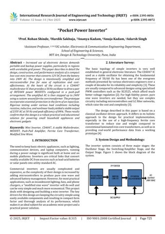
The inverter system consists of three major stages: the Oscillator Stage, the Switching/Amplifier Stage, and the Output Stage. Figure 1 shows the block diagram of the system.

International Research Journal of Engineering and Technology (IRJET) e-ISSN: 2395-0056

Volume: 12 Issue: 11 | Nov 2025 www.irjet.net p-ISSN: 2395-0072

Circuit diagram (Multisim):

1 Switching and Amplifier Stage:

Low-current square waves from the CD4047 cannot drive thetransformer.Therefore,thepoweramplificationstageis implementedwithapairofN-channelEnhancement-mode MOSFETs(IRFZ44N).TheseMOSFETswereselectedforvery low on-state resistance (RDS(on) = 17.5 mΩ), high drain currentcapability,andfastswitchingspeed.

TheQoutputpin10isconnectedtothegateofMOSFET1 T1,andQ'outputpin11isconnectedtothegateofMOSFET 2T2.

Inthisconfiguration,whenQison(high),T1activatesand allowscurrentfromthebatterythroughthefirsthalfofthe transformer's primary winding A-B and to ground. Correspondingly,whenQ'ison,theT2willturnonandsend currentthroughtheotherhalfoftheprimarywindingB-C, creating an alternating push-pull action that efficiently createsa50Hzalternatingmagneticfieldinthetransformer core.

2 Output and Protection Stage:

Theheartofthevoltageconversionisaspeciallywound, center-tappedstep-uptransformer.

 Primary Winding: 12V-0-12V.

 Secondary Winding: 240V.

Turnsratio=N_secondary/N_primary=240V/12V=20:1 Thealternatingmagneticfieldinducesa240VACvoltagein the secondary winding. A 5A fuse is in series with the positivebatteryinputforprotectionagainstcircuitdamage fromovercurrentorshort-circuitconditionsontheoutput.

3 Oscillator Stage:

The heart of the circuit is the CD4047 monolithic astable multivibrator.Itisconfiguredinitsastableoperatingmodeto generateacontinuoustrainofsquarewaves.Thefrequency ofoscillationispreciselydeterminedbytheexternaltiming components-a resistor, R1, and a capacitor, C1-connected betweenpins1,2,and3oftheIC.Thevaluefor50Hzoutput iscalculatedusingtheformula:

f

=1/(4.4*R1*C1)

With selected values of R1 = 220 kΩ and C1 = 0.1 µF the theoretical frequency is 50.5 Hz, which is well within the acceptable range. The CD4047 has two complementary outputs(QandQ')thatare180degreesoutofphase,whichis important for driving the subsequent push-pull amplifier stagewithoutcausingashortcircuit.

Component Selection and Justification:

Component Specification Quantity Justification

IC1 CD4047BE 1 Low-power, stableastable multivibrator.

T1,T2 IRFZ44NNChannel MOSFET 2 LowRDS(on), highcurrent capacity.

R1 220kΩ,1/4W Resistor 1 Timingresistor for50Hz frequency.

C1 0.1µF, PolyesterFilm Capacitor 1 Timing capacitorfor stable oscillation

TRANSFORM ER FerriteCore, 12-0-12Vto 240V,100W 1 Highefficiency, compactsize, reduced weight.

FUSE 5A,Quick-Blow 1 Overcurrent protection.

HEATSINK TO-220 Package 2 Todissipate heatfrom MOSFETs.

BATTERY 12V,7Ah SealedLeadAcid 1 StandardDC powersource.

4. Hardware Implementation: 1 PCB Design and Fabrication

Forreliabilityandcompactformfactor,asingle-sidedPCB wasdesignedusingKiCadEDAsoftware.Agreatdealofcare wastakeninthelayouttomakehigh-currentpathsfromthe

International Research Journal of Engineering and Technology (IRJET) e-ISSN: 2395-0056

Volume: 12 Issue: 11 | Nov 2025 www.irjet.net p-ISSN: 2395-0072

battery to the transformer as short/wide as possible to reducetheparasiticresistanceandinductance.

2 Assembly and Prototyping

Components were soldered to the fabricated PCB, paying muchattentiontopolarityfortheMOSFETsandcapacitor. TheMOSFETsweremountedonsubstantialaluminiumheat sinks. Thermal paste was applied to ensure efficient dissipationofheat.

5. Results and Discussion:

Theperformanceofaninverterprototypewastestedfornoloadanddifferentloadconditionsaftercompletion.Adigital multimeter,oscilloscope,andDCpowermeterwereusedfor measurementpurposes.

1 Waveform Analysis:

The output waveform was captured using a digital oscilloscope. Figure 5 shows the output under a no-load condition,clearlyshowingamodifiedsinewave-similartoa squarewave-at50Hz.

Performance Analysis under Different Loads:

3 Discussion of Results:

Thisindeedmetthedesignobjectivesoftheprototypeand converted12VDCintoapproximately240VAC.Becauseof transformerregulationcharacteristics,theno-loadvoltage washigher,about245V,whichisquitenormal.Underload, the voltage fell to a steady 235-239V, which is within the acceptablelimitsofmostappliances.

Thecalculatedefficiencypeakedatapproximately80%for the40Wfanload.Someofthemajorsourcesofpowerloss are:

1. Conduction Losses (I²R):

Because of the resistance of the transformer windingsandPCBtraces.

2. Switching Losses:

EnergylostinthefinitetimeittakestheMOSFETs toturnonandoff.

3. Core Losses:

Hysteresis and eddy current losses in the ferrite core of the transformer. The modified sine wave outputissuitableforresistive(bulbs)andinductive (fans,transformers)loadsbutmaynotbeidealfor

Fig -1:PCBdesignof100WMiniInverter
Fig -2:TestingResultof12VDcto240VAcInverter

International Research Journal of Engineering and Technology (IRJET) e-ISSN: 2395-0056

Volume: 12 Issue: 11 | Nov 2025 www.irjet.net p-ISSN: 2395-0072

sensitiveelectronicslikesomemedicalequipment oraudiodevicesthatrequireapuresinewave.

6. Conclusion and Future Scope:

Thisprojecthassuccessfullydemonstratedthedesignand implementationofafunctional,efficient,andlow-costmini inverter without using a microcontroller. Utilizing the CD4047 for a robust oscillator and power MOSFETs for efficient switching resulted in a compact and reliable prototype capable of powering essential low-power appliances.Thiscanserveasanexcellenteducationaltoolto understand how DC-AC conversion and power electronics work.

The following are suggested improvements for future enhancements:

Output Voltage Regulation: Afeedbackmechanismusinga comparatorandvariableresistorpotadjuststheoscillator frequency to provide a stabilized output voltage against battery discharge. Low Battery Cut-Off: Add a simple transistor/Zener diode circuit for the automatic disconnectionofthebatterywhenthevoltagefallsbelowthe specifiedsafetythreshold,say10.5V.

Audible Alarm: Incorporatingabuzzercircuittoalertthe userincaseoflowbatteryconditions.

Cooling Fan: Adding a small 12V DC fan triggered by a thermalswitchtoimprovethecoolingunderheavyloads.

References:

[1] S.R.SpeeandJ.H.R.Enslin,"Novellow-costinverter usingCD4047andMOSFETs," International Journal ofEngineeringResearchandTechnology(IJERT),Vol. 4,Issue02,February-2015,pp.773–777.

[2] M. H. Rashid, Power Electronics: Circuits, Devices & Applications,4thEdition,PearsonEducation,2014,

[3] A.S.Kulkarni,R.P.Havaldar,andS.S.Patil,"Design and Implementation of Low-Cost Inverter, International Journal of Innovative Research in Electrical, Electronics, Instrumentation and Control Engineering (IJIREEICE),Vol.6,Issue5,May2018, pp.134–138.

[4] Kale,PMoon,C Jadhav,V Patil,KJadhav,R Shinde. DistantMonitoringandControllingofGatedDams usingPLCandSCADA,Int.Res.J.Eng.Technol.,6(4), 2019,2900–2903.

[5] Texas Instruments, CD4047B CMOS Low-Power Monostable/AstableMultivibratorDatasheet,Revised September 2021. Available: https://www.ti.com/lit/ds/symlink/cd4047b.pdf

[6] Magare RA, Shinde RP, Badave SM (2022) A solarintegrated25-LEVELH-bridgemultilevelinverter.Int ResJEngTechnol[Online].www.irjet.net.

[7] R.K.Pongiannan,P.Sankardoss,andY.Paramasivam, "Designanddevelopmentofalowcostinverterfor educational purpose," Journal of Electrical Engineering,Vol.15,No.3,2015,pp.201–208.

[8] RohanPradeepShinde,“Differentinvertertopologies used to eliminate common mode ground leakage current” International Journal of Current Science (IJCSPUB)14(2),63-70

[9] V.ChawareandS.S.Chopade,"12VDCto230VAC Power Inverter using CD4047 and IRFZ44N MOSFETs," International Research Journal of Engineering and Technology (IRJET), Vol. 08, Issue 06,June2021,pp.2125–2129.

Turn static files into dynamic content formats.

Create a flipbook