
10 VIII August 2022 https://doi.org/10.22214/ijraset.2022.46016

Abstract: Serial devices are the fundamental building elements of all digital electronic systems with memory. The non volatile quality of sequential devices is necessary for quick data recovery after unexpected data loss, such as an unintentional power outage, which has sparked ongoing research and development into integrating a non volatile memristor into CMOS devices. In this article, we examine using this technique to raise the caliber of nonvolatile D latch. One memristor, a few transfer gates, and CMOS transducers are the sole components of the proposed D latch, which sets it apart from conventional designs. Our design minimizes the negative impact of transistor threshold loss. In addition, a variety of memristor threshold values are available with our Keywordsdesign.:Memristor, Transmission gates, D Latch and Flip flop. I. INTRODUCTION
2Associate Professor, Dept. of ECE, JSS Academy of Technical Education, Bengaluru, India
II. LITERATURE SURVEY
A. A nonvolatile latch circuit based on memristors." 235203 in Nanotechnology 21 & 23 (2010). Warren, Gilberto Medeiros Ribeiro, Qiangfei Xia, Greg Snider, Robinett, Matthew D.
1 M.Tech Student, Dept. of ECE, JSS Academy of Technical Education, Bengaluru, India.
International Journal for Research in Applied Science & Engineering Technology (IJRASET) ISSN: 2321 9653; IC Value: 45.98; SJ Impact Factor: 7.538 Volume 10 Issue VIII Aug 2022 Available at www.ijraset.com 297©IJRASET: All Rights are Reserved | SJ Impact Factor 7.538 | ISRA Journal Impact Factor 7.894 | Novel Memristor-based Non-volatile D Latch and Flip Flop Designs
Nagma Azmi Akbari1 , Dr. Mallikarjun S Swamy2
Volatile memory devices store data in various connection states and may therefore be employed in volatile computing systems. Excitation history affects the dynamic conduction state of these devices. The non volatile memory is a nanoscale memory device in this article's construction of a synchronous flip flop. State storage and retrieval are successful via controlled circuit testing. These results suggest that dispersed power sources and a combination of memristors and digital logic devices might enable nonvolatile computing on compact platforms. The traditional memoryhierarchyholds that non volatile memorycan only be accessed as a huge, slow monolithic at the bottom
Data security is critical and challenging in the age of big data because no one can predict where and when the next disruption will occur. Data backup technology is one of the most effective methods available now to reduce data loss and other harmful effects. Thus, the effectiveness of data backup and recovery determines whether the system can continue to operate continuously and stably. Data saved in volatile memory is moved to non volatile memory during the backup process and restored when the outage ends. System architecture and memorytype greatlyaffect data latency. The effectiveness ofdata backupdepends on howthisdelayisreduced.
Digital electronic systems rely on latching and latching devices as the building blocks. Volatile memory devices, such as traditional flip flops, lose their data when their power is cut. A varietyofmethods are used tokeep the heart in an intermediate state of operation. Therehas recently been a lot of interest in a revolutionary technique that uses flip flops to store volatile material and a variety of new memory technologies, such as electro transistor, torque magnetic RAM, phase change RAM, and ferroelectric RAM.Toimprove the design and data backup quality of CMOS flip flops, these solutions use non volatile memory components and control circuitry. Delay time and energy consumption areboth reduced. One ofthesenewmemories isthe memristor, which stands for memoryresistance. Itwas predicted byLiu Chua in 1971[1]and modeled by HP Lab in 2008 [2]. In addition to their low power consumption, high density, and efficient integration, these nonvolatile devices also have the advantage of being very compatible with CMOS devices, all of which have been examined. The use of memristors in the memory components also makes non volatile memory affordable and able to store intermediate stages fast. A brief history of prior attempts to develop locks andslippersbased onmemoryis then provided. The goal of this effort is to find ways to increase the robustness of these advanced memristor based designs while retaining the benefits of volatility. We propose a level sensitive, non volatile Dlatch based on memristors similar tothat in [7], but with the following improvements: a much larger threshold voltage range for the I memristor; (ii) low latency; and (3) improved robustness against supplyvoltage fluctuations. Comparedtoprevious designs, this D latch basedmaster slaveDFF performsbetter intermsofspace andlatency.


B. Zero Sleep Leakage Flip Flop Circuit with Conditional Storing Memristor Retention Latch," in IEEE Transactions on Nanotechnology C. M. Jung, K. H. Jo, E. S. Lee, H. M. Vo and K. S. Min
III.METHODOLOGY
Memristors with very fast switching times are becoming increasingly popular with the development of non volatile memory based on resistive switching. On the other hand, according to the research mentioned above, memristors with modest switching times (around 10 seconds) are more suitable for use in nervous systems. This is achieved by simulating different types of memories with different switching times. Using each of these model components, a neural circuit based on memristors is simulated. To slowly adjust the memristor resistance in devices withhigh switchingspeeds, unreasonablylowvoltagepulses arerequired.
To effectively eliminate sleep leakage, two innovative non sleep leakages (F F) flip flop (F F) circuits have been developed. Data is sent from the F F to the memristor retention latch during sleep, preventing the F F from being completelydisconnected from the external power source and power leakage during sleep. Compared to F F, the conditional storage circuit of F F (Type 2) can use less switching power to store data (Type 1). Additionally, comparedtoF F, F F (type 2) hasa shorter crossover time (type 1).
Different from the conventional SR flip flop and D flip flop circuits which consist of several logic gates, the proposed nonvolatile synchronous SR flip flop and D flip flop, discussed in this work, is based on the combination of CMOS and threshold type voltage controlled bipolar memristors. This section explains the topologies and operating principles of the flip flops.
International Journal for Research in Applied Science & Engineering Technology (IJRASET) ISSN: 2321 9653; IC Value: 45.98; SJ Impact Factor: 7.538 Volume 10 Issue VIII Aug 2022 Available at www.ijraset.com 298©IJRASET: All Rights are Reserved | SJ Impact Factor 7.538 | ISRA Journal Impact Factor 7.894 | of the hierarchy, however, the ability to tightly integrate memristors with CMOS (complementary metal oxide semiconductor) circuits undermines this assumption. Non volatile memory cells built on memristors are fast, accurate, and compact enough to be integrated into standardCMOScircuits. Asaresult,the traditionalmemoryhierarchyis puttothe test,andnewdesign possibilities aremadeavailable.
D. Determining optimal switching speed for memristors in the neuro morph systems stem. Electronics Yakopcic, C. &Taha, T.M. (2015).
The schematic of the memristor is shown in Fig, bottom terminal is denoted by the black thick line. The memristance will decrease when the forward bias voltage is applied to acrthe oss memristor, and it will increase when the memristor is reversely biased. In Fig, we show the qualitative current voltage characteristic of the threshold type switching memristor. When the applied voltage is larger than the positive threshold VSET, the memristance switches to RON. Then, when the applied voltage is smaller than the negative threshold VRESET, the memristance returns to ROFF. If the applied voltage is in between VRESET and VSET the memristance will remain unchanged. Therefore, the memristor's two distinctive resistance states can represent logic 0 and logic 1. The binary data can be written to the memristor through a writing voltage, and the data stored in the memristor can also be read by a small reading voltage so that the states will not be lost even if the power is off Fig: (a) The schematic of the memristor. (b) The qualitative current voltage characteristic of the threshold type switching memristor.
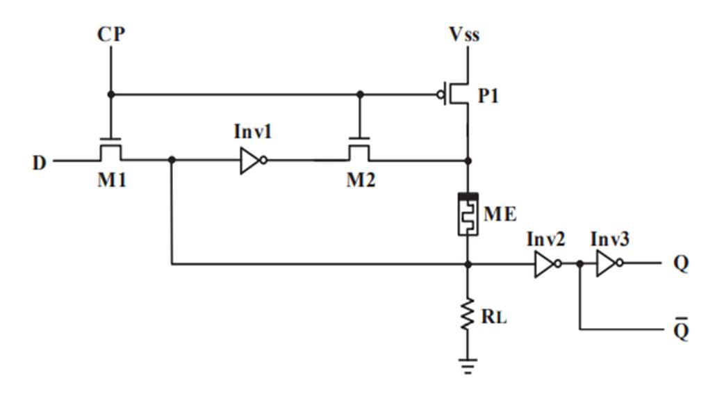
C. Memristor based nonvolatile synchronous flip flop circuits J. Zheng, Z. Zeng, and Y. Zhu Flip flops are crucialparts ofall varieties ofsequentiallogic circuitsandsophisticated digital electronics systems andmaybe utilized tostore binarydata due to their two stable logic states of 0 and 1. Digital circuits often make use of SR and D flip flops as examples of basic base flips. This work introduces non volatile synchronous SR flip flop and D flip flop synchronous logic circuits that use non volatile nano memristors with various conduction states for data storing. components of memory. Memristors are the best choice for flip flop circuits that need trigger functions since theycan substituteresistors. In contrast totraditional flip flops, the memristor based SR flip flop andD flip flop have non volatile properties that make them appropriate for applications with erratic power sources. Advanced circuits serve as empirical benchmarksfor creatingdigital circuittopologies because tightmemristor integration with CMOScircuitsis feasible.
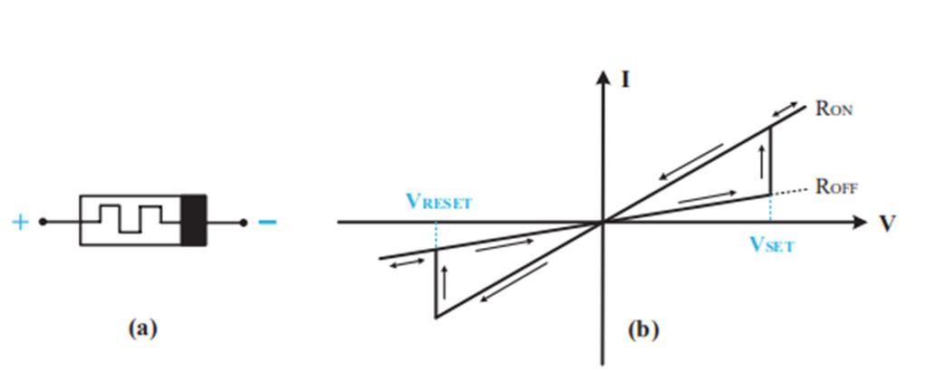
Fig: Proposed memristor based nonvolatile synchronous D flip flop circuit
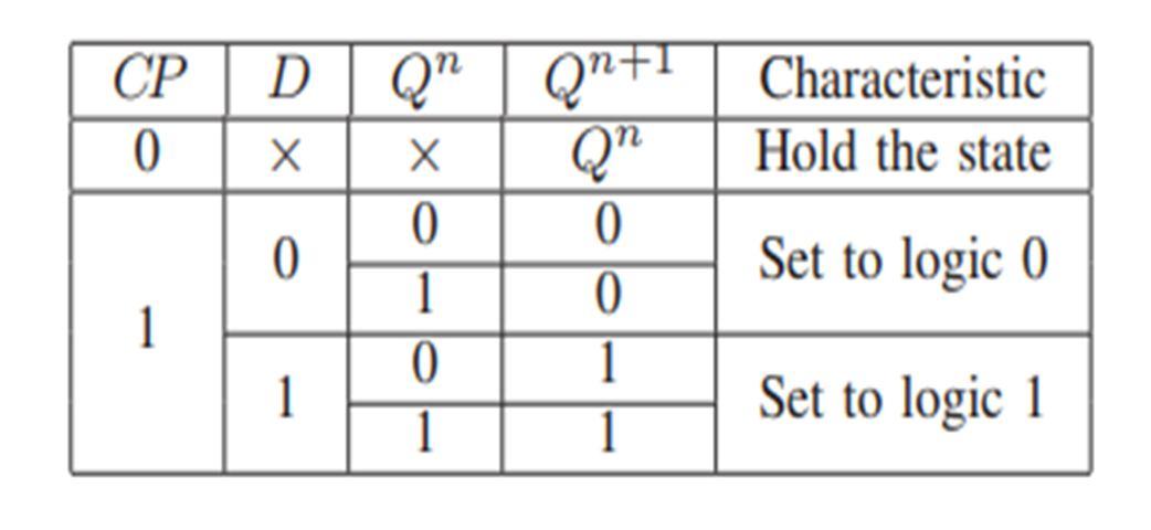
The components of the circuit include a threshold type memristor (ME), a resistor (RL), NMOS transistors (M1, M2), a PMOS transistor (P1), and inverters (Inv1, Inv2, Inv3). Its operation principles and circuit structure are similar to the SR flip flop presented in Section II B. When the CP is at logic 0, the M1 and M2 turn off while P1 turns on, so changes at the D input make no difference to the Q and Q¯. Similar to the SR flip flop, the Q will remain unchanged. When the CP is at logic 1, then P1 turns off while M1 and M2 turn on. If the D input goes to logic 0 (logic 1), the Q is logic 0 (logic 1) since the output terminal of Q is connected to the input terminal of D. Also, the input of Inv2 is logic 0 (logic 1) and the output of Inv1 is logic 1 (logic 0), causing RME to be switched to ROFF (RON) that the Q sets to logic 0 (logic 1) when the CP changes from high to low.
Table: Truth table of D Flip flop
International Journal for Research in Applied Science & Engineering Technology (IJRASET) ISSN: 2321 9653; IC Value: 45.98; SJ Impact Factor: 7.538 Volume 10 Issue VIII Aug 2022 Available at www.ijraset.com 299©IJRASET: All Rights are Reserved | SJ Impact Factor 7.538 | ISRA Journal Impact Factor 7.894 | A. SR Flip Flop Circuit Architecture and Operations
B. D Flip Flop Circuit Architecture and Operations
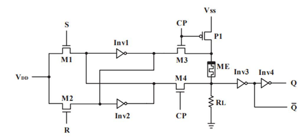
We proposed a memristor based nonvolatile synchronous SR flip flop circuit. It consists of a threshold type memristor (ME) connected in series to a pulldown resistor (RL), two pairs of NMOS transistors (M1, M2, M3, M4), a PMOS transistor (P1), and four inverters (Inv1, Inv2, Inv3, Inv4). The set voltage is applied to S and the reset voltage is applied to R. The CP controls the switch states of M3, M4, and P1 and different transistor states can form different equivalent circuit structures to achieve different trigger functions of SR flip flop. Compared with traditional SR flip flop circuits, the new circuit structure is not only simpler but also has nonvolatility.
Fig: Proposed memristor based nonvolatile synchronous SR flip flop circuit
C. This design is not suitable for high clock frequency
B. The time for the memristor switching between different states is increased as reducing the writing voltage on the memristor will always increase the switching time of the memristor.
A. When the clock signal presents high, due to the voltage allocated on the transistors M1 and M2, usually called threshold loss, the voltage in the memristor is reduced.
.
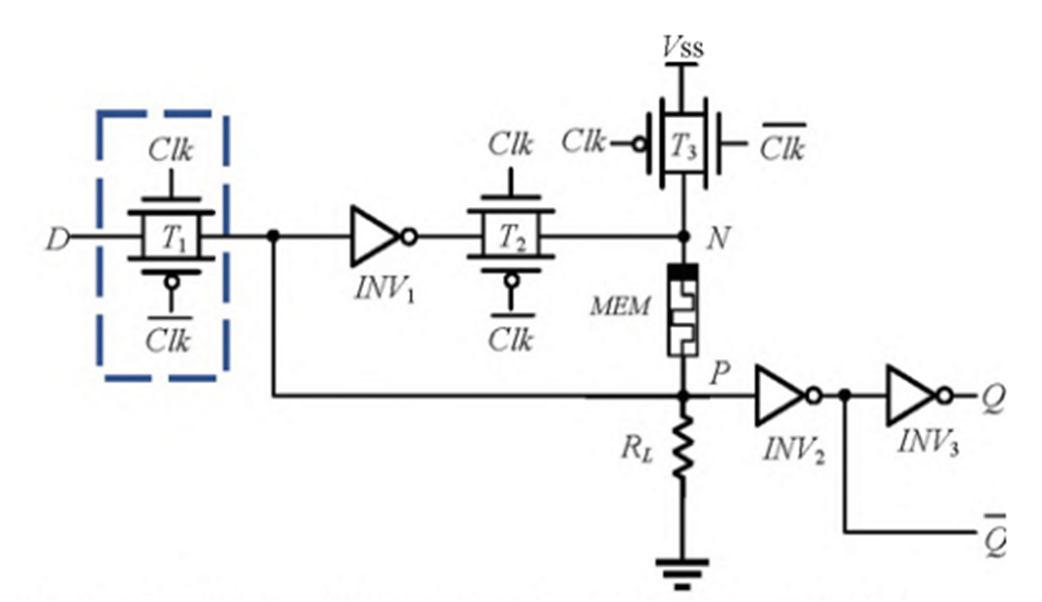
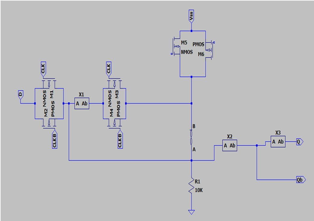
The structure of the proposed D latch design: Fig: Memristor based D Latch A transmission gate (the dashed box in Figure) is composed of a complementary pair of transistors and can control the transfer of logic levels from one node to another when its control signals are activated As the threshold loss is prevented by the transmission gate, the output Q = D, which we refer to as the writing phase. When D = ‘0’, the inverter INV1 outputs ‘1’ at point N and the point P presents as ‘0’. Thus, the voltage from the positive terminal of MEM to the negative terminal of MEM equals Vcc. As Vcc<Vreset, the resistance state of the memristor MEM switches to Roff. Similarly, when D = ‘1’, the voltage from the positive terminal of MEM to the negative terminal of MEM equals Vcc. As Vset <Vcc, the memristor switches to Ron state.
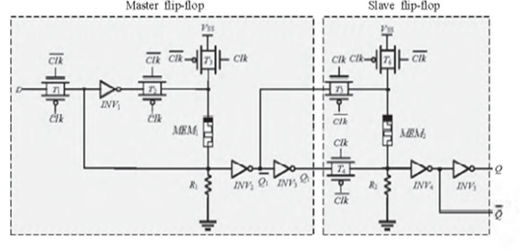
A. Memristor based D Type Master Slave Flip Flop
In this section, we discuss how to use the above proposed memristor based D latch to build a D master slave flip flop. For an enabled level sensitive flip flop, its content changes instantaneously when its input changes. i.e., when enabled, the input determines the output instantly. Therefore, the level sensitive flip flops are vulnerable to disturbance in the input signal and cannot be widely used in large scale digital integrated circuits. In comparison, flip flops have their content changes only either at the rising edge or falling edge of the clock signal. After the rising or falling edge of the clock, the flip flop content remains constant even if the input changes. Thus, the flip flop is less vulnerable to noise than the latch.
International Journal for Research in Applied Science & Engineering Technology (IJRASET) ISSN: 2321 9653; IC Value: 45.98; SJ Impact Factor: 7.538 Volume 10 Issue VIII Aug 2022 Available at www.ijraset.com 300©IJRASET: All Rights are Reserved | SJ Impact Factor 7.538 | ISRA Journal Impact Factor 7.894 | IV. DISADVANTAGES
Fig: circuit diagram of memristor based D Flip flop
V. PROPOSED SYSTEM We present in this section the design, analysis, and simulation results of our nonvolatile D type latch based on a memristor that can support high clock frequency.
The simulation of the proposed master slave DFF design and Memristor based DFF design
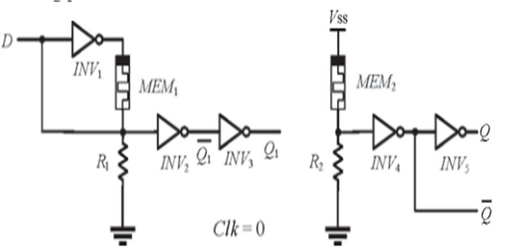
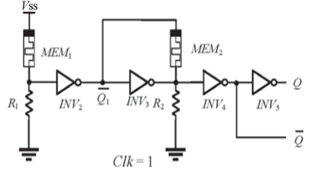
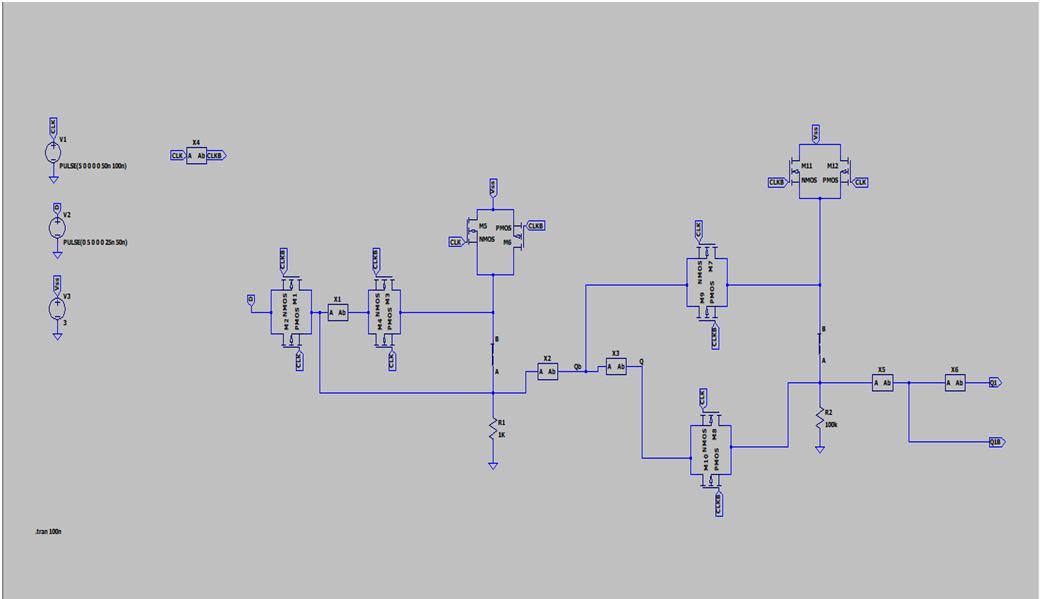
Fig: Equivalent design when clk=0 Fig: Equivalent design when clk=1. When the Clk is low, T1, T2, and T6 are turned on while T3, T4, and T5 are turned off. The equivalent circuit is shown in Figure.
International Journal for Research in Applied Science & Engineering Technology (IJRASET) ISSN: 2321 9653; IC Value: 45.98; SJ Impact Factor: 7.538 Volume 10 Issue VIII Aug 2022 Available at www.ijraset.com 301©IJRASET: All Rights are Reserved | SJ Impact Factor 7.538 | ISRA Journal Impact Factor 7.894 |
The master flip flop works in the writing phase and the input D is latched in the master flip flop by changing the resistance state of the memristor MEM1. This state is isolated from the slave flip flop which works in the reading phase. The output Q keeps consistent with the resistance state of MEM2 but not the input D. If MEM2 presents as Roff /Ron, the output signal Q = ‘0’/ ‘1’ When the Clk signal is high, the T3, T4, and T5 are turned on while T\, T2, and T6 are turned off. The equivalent circuit is shown in Figure 8(b). The master flip flop enters the reading phase while the slave flip flop is activated to work in the writing phase. The content in the master flip flop is fetched into the slave flip flop and output to Q. If MEM\ presents in Rof f /Ro n state, the output signal Q = ‘0’/ ‘1’. Meanwhile, the value determines the resistance state of MEM2. Based on the analysis above, the output of the proposed DFF only changes when the clock transits from low to high. In other words, the master slave flip flop captures the input signal on the rising edge of the clock while maintaining the state for the rest time. It also inherits the nonvolatile property of the proposed latch.
Fig. Schematic of memristor based Master slave flip flop
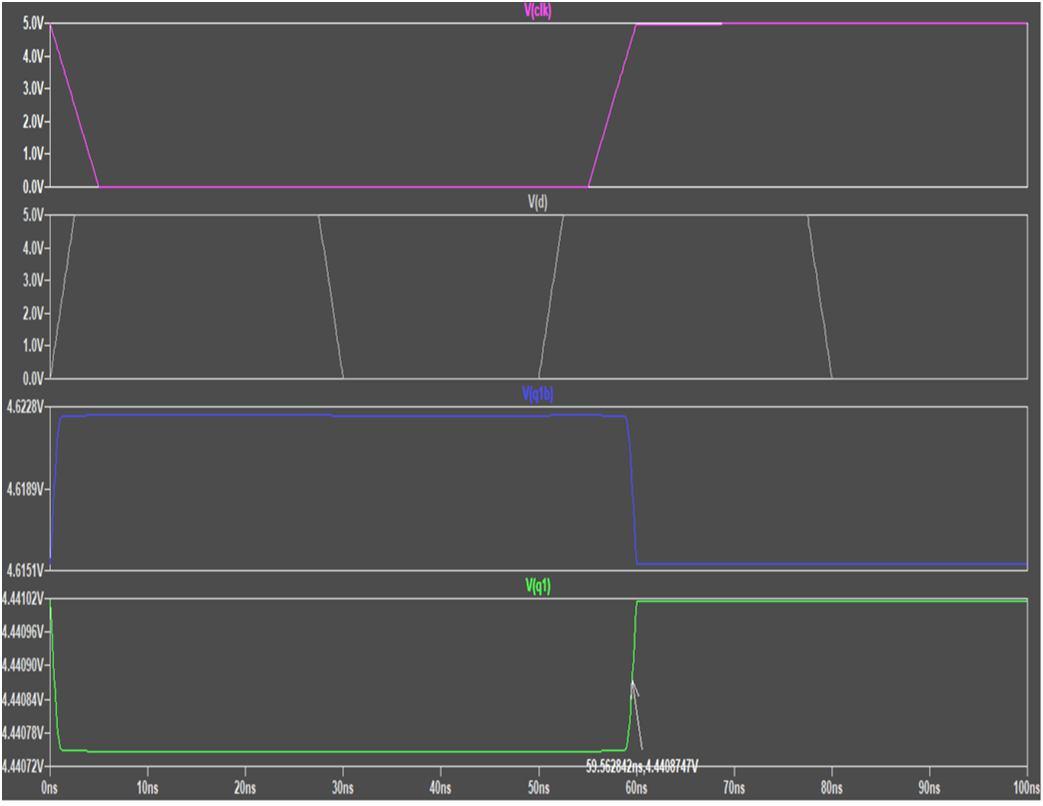
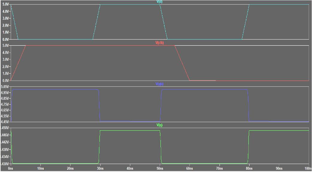
International Journal for Research in Applied Science & Engineering Technology (IJRASET) ISSN: 2321 9653; IC Value: 45.98; SJ Impact Factor: 7.538 Volume 10 Issue VIII Aug 2022 Available at www.ijraset.com 302©IJRASET: All Rights are Reserved | SJ Impact Factor 7.538 | ISRA Journal Impact Factor 7.894 | Fig.Output waveforms of Memristor based Master slave flip flop Fig. Schematic of Memristor based D Latch Fig.Output waveforms of Memristor based D Latch VI. ADVANTAGES & APPLICATIONS A. Our design realizes a faster switching of the resistance state of the memristor. B. Enables the latch to support a clock of higher frequency. C. It improves the capability of the design to resist disturbance in supply voltage. D. Data backup technology.
[10] Yakopcic, T. M. Taha, “Determining optimal switching speed for memristors in the neuromorphic system,” Electronics Letters, vol. 51, no. 21, 2015, pp. 1637 1639 [11] Harry J. M. Veendrick, Nanometer CMOS ICs: From Basics to ASICs, Springer, Heidelberg, Germany, 2008, pp. 190 191.
[8] MT Arafin, C Dunbar, G Qu, N McDonald, L Yan, “A survey on memristor modeling and security applications”, in Proc. 16th International Symposium on Quality Electronic Design), Santa Clara, CA, March 2015, pp. 440 447, [9] Biolek, M. D. Ventra, and Y. V. Pershin, “Reliable SPICE simulations of memristors, memcapacitors, and meminductors,” Radioengineering, vol. 2 2, no. 4, July 2013, pp. 945 968.
[4] M. Jung, K. H. Jo, and E. S. Lee, “Zero Sleep Leakage Flip Flop Circuit with Conditional Storing Memristor Retention Latch,” IEEE Transactions on Nanotechnology, vol. 11, no. 2, March 2012, pp. 360 366.
[5] I Kazi, P. Meinerzhagen, and P. E. Gaillardon, “A ReRAM based non volatile flip flop with sub VT read and CMOS voltage compatible write,” in Proc. 2013 IEEE 11th nternational New Circuits and Systems Conference (NEWCAS), Paris, France, 2013
[2] B. Strukov, G. S. Snider, and D. R. Stewart, “The missing memristor found,” Nature, vol. 453, 2008, pp. 80 83.
VII. CONCLUSION Based on this new latch in this work, we propose an improved D type latch based on memristor and non volatile flip flop. Only a few transfer gates, CMOS converters, and memristor make up the proposed latch. Our approach achieves faster memristor impedance state switching than memristor based latches, allowing the latch to handle a high frequency clock. In addition, it increases the design's resistance to voltage fluctuations. Based on the proposed latch, master and slave non volatile DFF are kept. According to the simulation results, the suggested DFF has better timing performance than previous memristor based DFFs. The footprint is also smaller than all but one of the existing memristor based DFF designs. REFERENCES
[1] L. Chua, “Memristor The missing circuit element,” IEEE Transactions on Circuit Theory, vol. 18, no. 5, January 1971, pp. 507 519
[3] W. Robinett, M. Pickett, and J. Borghetti, “A memristor based nonvolatile latch circuit,” Nanotechnology, 21(23):235203, May 2010, pp. 1 6.
[7] J. Zheng, Z. Zeng and Y. Zhu, “Memristor based nonvolatile synchronous flip flop circuits,” in Proc. 2017 Seventh International Conference on Information Science and Technology (ICIST), Da Nang, May 2017, pp. 504 508.
International Journal for Research in Applied Science & Engineering Technology (IJRASET) ISSN: 2321 9653; IC Value: 45.98; SJ Impact Factor: 7.538 Volume 10 Issue VIII Aug 2022 Available at www.ijraset.com 303©IJRASET: All Rights are Reserved | SJ Impact Factor 7.538 | ISRA Journal Impact Factor 7.894 |
[6] H. Sun, X. Xu and H. Shao, “Memristor based nonvolatile D trigger,” CN 103051307 A[P]. 2013