
10 X October 2022 https://doi.org/10.22214/ijraset.2022.47245
ISSN: 2321 9653; IC Value: 45.98; SJ Impact Factor: 7.538
Volume 10 Issue X Oct 2022 Available at www.ijraset.com

ISSN: 2321 9653; IC Value: 45.98; SJ Impact Factor: 7.538
Volume 10 Issue X Oct 2022 Available at www.ijraset.com
1Assistant Professor, Electronics and Communication Engineering, Institute of Aeronautical Engineering College, Hyderabad 2, 3, 4B.Tech Students, Electronics and Communication Engineering, Institute of Aeronautical Engineering College, Hyderabad

Abstract: The Portable electronic gadgets have turned into a major part of life. Electronic gadgets predominantly consist of arithmetic units. A full adder is an important part of arithmetic units like multipliers. In order to enhance the rate and efficiency of such systems, it is worthwhile to design a FA that has higher rates of speed and low consumption of power. A Full adder circuit is frequently implemented using a hybrid logic approach. This work proposes a 10T XOR-XNOR circuit which shows improved delay performance. The suggested circuit's performance is determined by modeling that circuit in a virtuoso platform powered by cadence by using 18 nm FinFET technology. Additionally, here four distinct designs of a full adder are presented by making use of the proposed XOR-XNOR circuit and the available sum and carry modules. These circuits show an improved PDP when simulated using FinFET technology than CMOS technology.
Keywords: Cadence, FinFET, CMOS, PDP, Hybrid Model.
Full adder is the most essential component found in majority of the digital signal processors used in real time applications. Adders are also used in the design of other arithemetic operators like subtractor, multiplier, shifter, MAC, etc. Many researchers have proposed many advanced designs over the years. Even now, Adder architecture research is gaining popularity as a means of developing energy efficient products. The assessment of traditional adder designs revealed that there is a lot more room for optimization. One method of optimization is designing the circuit using a hybrid design approach, where a full adder can be designed with modules.
In a classic design approach, the full adder is outlined as one module by making use of MOS transistors. One of the examples of the classic design style is the Complementary CMOS Full Adder (CCMOS). That circuit has 28 transistors to perform the pull up and pull down functions in theadder. This design shows us full swing yields, but the main disadvantage comes when the input capacitances arehigher because of the inputs connected at the gates with a pMOS and an nMOS transistor due to which the adder’s speed and performance are degraded. One more well known design typeis the complementary pass transistor logic (CPL) complete adder. Due to the high speed differential stage, cross coupled pMos construction, and static inverter at the output, this design also delivers full swing outputs, high speed, and strong driving capabilities. The circuit’s disadvantages include excessive power dissipation due to the presence of a large number of internal nodes. Because of the uneven transistor configurations, the circuit architecture is likewise asymmetrical.
Full adders can be designed using pass transistors in classical design approach. Even though the pass transistors have built in pinch off voltage drop issues. Whenever the logic “1” and logic “0” are given to nMOS and pMOS as inputs, we could not obtain full swing logic “1” and logic “0” as outputs. This problem can be solved using a transmission gate (TG) based solution. One nMOS transistor and one pMOS transistor are coupled in parallel and controlled by additional control signals in this design. These pMOS and nMOS are switched on at the same time and give routes to both the logic (logic "1") and the full swing outputs (logic "0"). Although the TG based adder consumes less power, it has limited driving capabilities. Using output buffers can improve circuit performance
ISSN: 2321 9653; IC Value: 45.98; SJ Impact Factor: 7.538 Volume 10 Issue X Oct 2022 Available at www.ijraset.com
In the hybrid design style, a circuit is implemented in many modules. For designing a full adder using the hybrid approach, three modules are used. The first module takes two input signals and generates a full swing XOR XNOR outputs simultaneously. The XOR XNOR outputs become the input to the next two modules. The second and third modules are used to generate sum and carry outputs. The key advantage of the hybrid approach is that each module can be implemented individually, reducing the number of transistors and hence the internal power dissipating nodes. The main aim of using a hybrid design style is to save space, volume, and weight compared to the classical design style. Through this, we can also achieve very good results with low power and delay and very high reliability. This makes hybrid circuits suitable for various applications in our daily life making life easier with better performances. They are also used in military systems, space applications, medical electronics, as well as computers, and telecommunication equipment.
Several researchers have developed FA systems that use a mixed logic approach to give an optimal performance without affecting output. A pass transistors logic (PTL) XOR XNOR module is shown, with sum and carry units executed using a 2 to 1 multiplexer circuit [1]. PTL is employed to create XOR XNOR outputs concurrently, and the C CMOS method is made used to build the carry unit in a hybrid FA cell [3]. One of the designs is a New low power and high speed (LPHS) adder, that uses a feedback transistor to build the XOR XNOR unit, while the sum and carryunits use PTL and a 2 to 1 multiplexer,respectively [7]. The performance of the XOR XNOR circuit is critical tothe hybrid FA design’s success. In recent years, many ways to create XOR XNOR circuits have been published. Thesemethods may be divided into two groups. The XOR unit is first implemented, and next one extra buffer [example: transmission gate adder (TGA)] is used to create the XNOR output. This method has the disadvantage of not generating XOR and XNOR outputs concurrently, this raises risk of erroneous glitches and switching in the outputs of modules II and III [7].
Considering a different method, here the XOR XNOR circuit is created to show both the XOR and XNOR outputs atthe same time. The difference in delays of XOR and XNOR signals is attempted to be reduced in this manner. A CPL based XOR XNOR circuit is given, allowing for simultaneous creation of XOR XNOR outputs [5]. The feedback transistors in this design restore the output voltage levels. The feedback transistor, however, keeps the circuit’s delay and power greater. The NOT gate is removed from the critical path, but due to the cross coupled arrangement, the circuit delay remains larger [5]. With only six transistors, another XOR XNOR circuit is demonstrated. When both inputs have the same value (either "00" or "11"), two complementary feedback transistors are employed to restore the weaker logic in complementary output nodes (XOR and XNOR) [2].
For inputs "11" or "00," as in these examples, this circuit has a long worst case delay; out puts come to their last potential values in the two stages. Two extra nMOS and pMOS transistors are used at the XOR and XNOR output intersections, respectively, to address the issue of delayed response [4]. This circuit has a lot of driving power and a wide output swing. The cross coupled arrangement, on the other hand, adds additional parasitic capacitance to the XOR XNOR output intersections.
The use of an inverter improves the structure of an XOR XNOR circuit [9]. Although this arrangement reduces critical route latency, power dissipation remains substantial.The XOR XNOR circuit is enhanced and built utilizing 12 transistors. This circuit uses less power and performs better in terms of delay than the others. This circuit, however, requires an additional inverter [10]. By removing the external inverter, the circuit's performance may be increased even further.
ISSN: 2321 9653; IC Value: 45.98; SJ Impact Factor: 7.538 Volume 10 Issue X Oct 2022 Available at www.ijraset.com
In our proposed method, the full adders are designed using hybrid style logic method. In general, in a hybrid logic fashion, the circuit is divided into modules. Here, the complete add on circuit is categorised into three modules as depicted in the below Figure 3.1. The first module generates the outputs of XOR XNOR, the second module generates the sum result, and then third module provides the output of carry. Each module is individually designed and then combined into a full adder. Full adder is then implemented in FinFET. Then power and delay are measured.
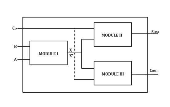
Fig. 2. Block diagram of FA using hybrid logic style

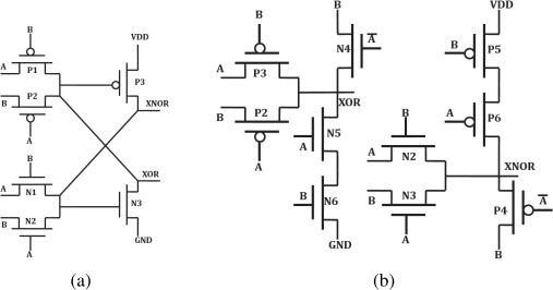
Several ways to create XOR XNOR circuits have been suggested in recent years, which are detailed in the previous chapter. An XOR XNOR circuit has been proposed that produces a full swing output with just six transistors. The CPL and feedback restorer transistors are used to realize this design. This design provides a good performance for the inputs A,B: 0,1 and 1,0 in terms of delay. However, it has a switching delay at the output for the inputs A,B: 1,1 and 0,0. The increased delay for these inputs is handled by including two nMOS and two pMOS transistors in the circuit. The latter solution overcomes the slow response problem and also minimizes the circuit's power consumption. It utilizes ‘A’ as an input, which necessitates the employment of an additional inverter. This section proposes a new XOR XNOR circuit that creates the inverted input internally without the use of an external inverter. This configuration decreases the number of transistors in the circuit as well as the total number of internal nodes get decreased, by lowering the total delay and power consumption of the circuit. The proposed XOR XNOR circuit with 10 transistors that provide full swing outputs is depicted in fig 3.2. The suggested XOR XNOR circuit has a cross coupled construction and is based on CPL. Two pMOS transistors (P1 and P2) and three nMOS transistors (N3, N4 and N5) are used on the output side of XOR, and two nMOS transistors (N1 and N2) and three pMOS transistors (P3, P4 and P5) on the output side of XNOR. P1 and P2 are linked parallelly as PTL on the XOR side, with N4, N5, and N3 acting as restorers to produce a full swing output and transistor N3 acts as a feedback transistor. Transistors N1 and N2 are connected parallely as PTL, P4, and P5 are connected as a restorer to generate a full swing output, and transistor P3 is connected as a feedback transistor on the XNOR output side. This circuit simultaneously produces full swing XOR XNOR outputs.
ISSN: 2321 9653; IC Value: 45.98; SJ Impact Factor: 7.538 Volume 10 Issue X Oct 2022 Available at www.ijraset.com
By considering the Cin and outputs of the previous XOR XNOR cell as inputs the summing cell is executed. Then the sum outputs are produced. Here are the proposed four designs of this module which are depicted in the following fig 4.
Fig. 4. Module II circuit using (a) Transistor Gate, (b) Transistor Gate with inverter design 1, (c) Transistor Gate with inverter design 2, and (d) CMOS.
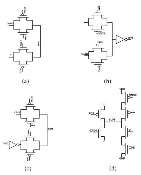
SUM circuit, illustrated in Fig. 4(a), is made up of four transistors and uses TG as a 2 to 1 multiplexer. The XOR and XNOR yields are utilized at the gate as inputs, while Cin and Cin are used as inputs to the sources of two TGs in the circuit. This circuit provides us the high speed and the consumption of power is very less with a complete output swing. However, because of the formation of parasitic capacitance and resistance during creation, this circuit has an issue with driving capabilities. As illustrated in Fig. 4, the issue of driving capability may be solved by utilizing an inverter at end of the output (b). However, using extra inverter results in higher power consumption and increased delay. A buffer (Cin followed by an inverter) is utilized at the input side of another form of SUM circuit construction, as illustrated in Fig. 3.3 (c). The circuit's driving capability is boosted by employing the buffer at the inputs. The buffer at the input recovers the preceding stage's deteriorated output level. Figure 3.3 shows a SUM circuit based on CMOS logic. (d). This circuit, which employs six transistors, has a high driving capability and resilience.
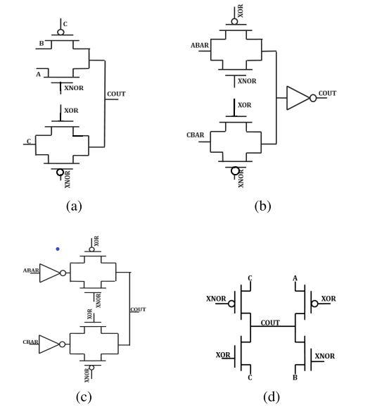
A carry circuit is the FA's third module (Cout). The FA's output carry may be estimated using the XOR and XNOR outputs of module I, as well as prior, carry Cin. The researchers have offered numerous designs for this module. Module III's four designs are depicted in the following fig 5.
Fig. 5. Module III circuit using (a) Transistor Gate, (b) Transistor Gate with inverter design 1, (c) Transistor Gate with inverter design 2, and (d) CMOS.
ISSN: 2321 9653; IC Value: 45.98; SJ Impact Factor: 7.538 Volume 10 Issue X Oct 2022 Available at www.ijraset.com
This module is designed by utilizing the multiplexer in most adders, as seen in Figure. 3.4 (a). Cout is formed in this circuit by sending the value of either A (or B) or Cin at the output based on intermediate signals (module I's XOR and XNOR outputs). To obtain greater driving capacity, one buffer is placed at either input or output side, as illustrated in Fig. 3.4 (b) and 3.4 (c), respectively. However, it increases the whole circuit's power consumption and latency. Figure 3.4 depicts a CMOS based module III (d). It has four transistors, consumes less power, and has greater delay performance.

As explained, a hybrid FA may be created by merging three modules (the XOR XNOR circuit as a module I, the summing circuit as module II, and the carry circuit as module III). In the previous section, a unique XOR XNOR circuit is introduced, while prior sections examined certain module II and module III circuits. Four designs of hybrid logic style based FAs are provided in this part by combining the suggested XOR XNOR circuit with four alternative modules II and Module III circuits.
The proposed FA 1 is implemented using finFET technology as shown in figure 4.2. The outputs of 1st module generate full swing outputs resulting in giving better inputs to the sum and carry module. This circuit has 20 transistors. It delivers full output swing and high robustness as there is no external inverter used the no of transistors used is only 20.
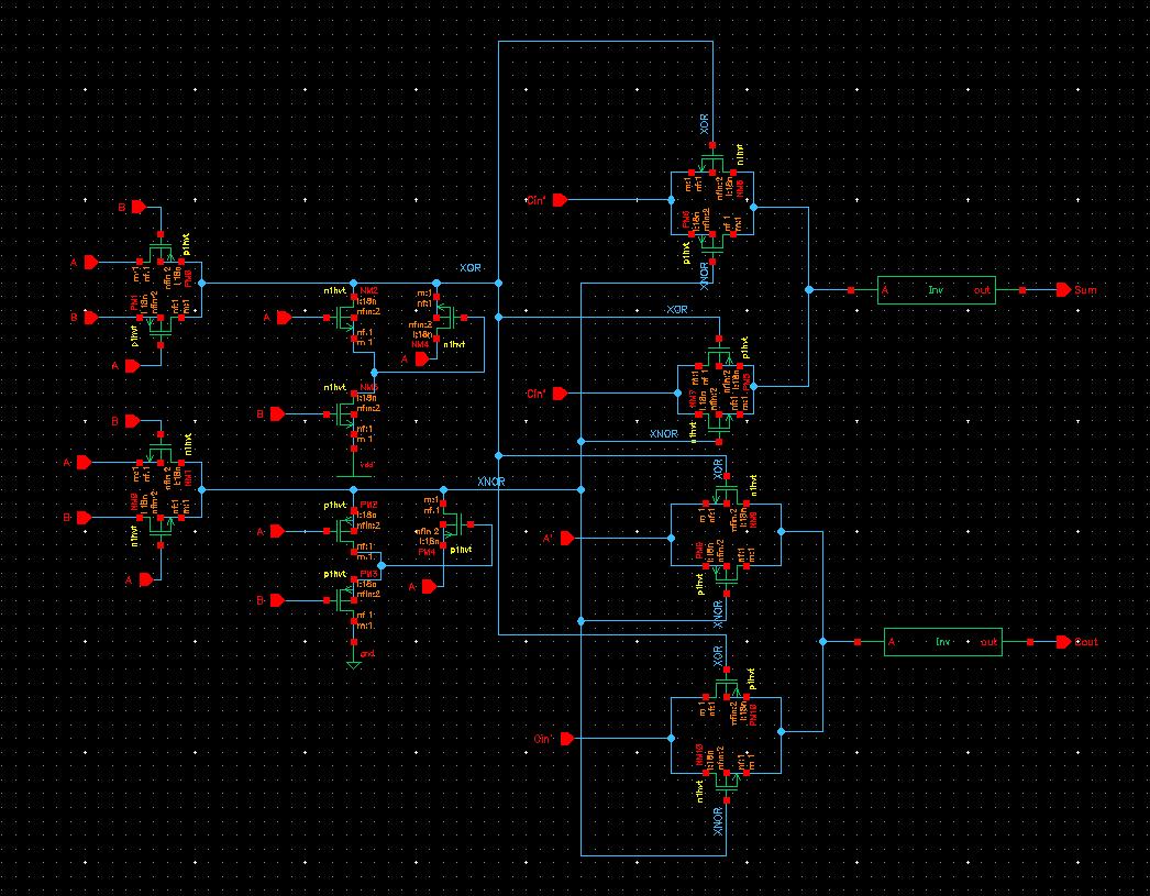
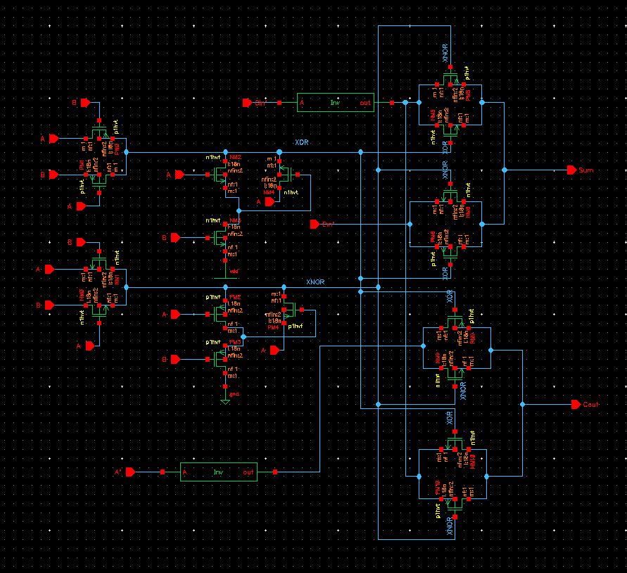
The proposed FA 2 is implemented using finFET technology. This hybrid circuit consists of three modules i.e., 1. XOR XNOR, 2. Sum, 3. Carry. The outputs of the first module(XOR XNOR) are provided as inputs to the next modules. The outputs of 1st module generate full swing outputs resulting in giving better inputs to the sum and carry module. In FA 2, we implement using 26 transistors, as shown in fig 7. In this design, we use inverters at the output of module II and module III resulting in decreasing driving capability.
Fig. 7. Proposed FA 2 circuit
ISSN: 2321 9653; IC Value: 45.98; SJ Impact Factor: 7.538 Volume 10 Issue X Oct 2022 Available at www.ijraset.com
The proposed FA 3 is implemented using finFET technology as shown in figure 4.4. This hybrid circuit consists of three modules i.e., 1. XOR XNOR, 2. Sum, 3. Carry. The XOR XNOR outputs are provided as inputs for the sum and carry modules along with the A, B, and Cin. The outputs of 1st module generate full swing outputs resulting in giving better inputs to the sum and carry module. In this circuit, we are using two buffers at the inputs. Due to the usage of buffers, the power consumption is increased and also the delay is affected. We use inverters at the input side of module II and module III. The FA 3 circuit consists of 26 transistors.
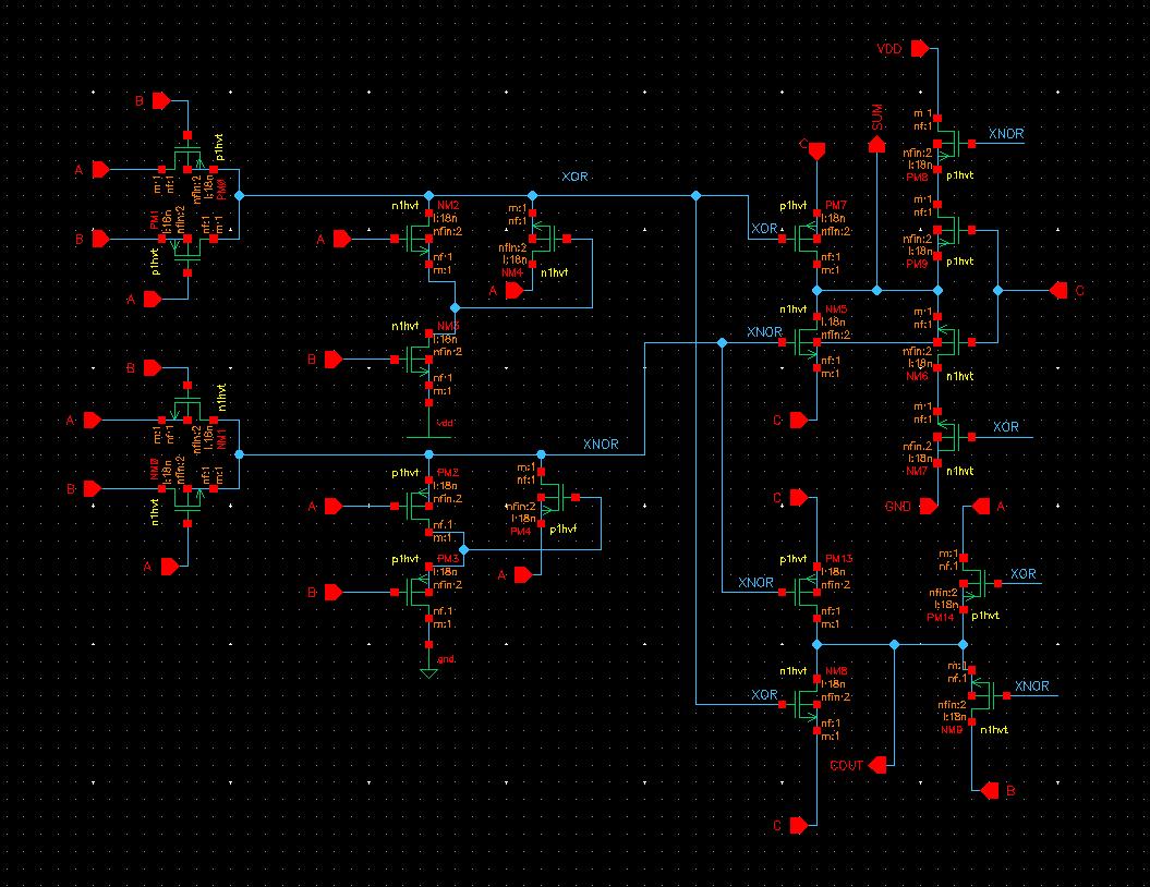
The FA 4 design also uses three modules in producing the outputs but the design of this adder is different from the other three adders. Module II and Module III are implemented using the CMOS design logic style, as shown in fig 4.5. The circuit does not have any external inverters. This full adder design provides the best performance in terms of power consumption and delay.
In FinFET Technology From the current technique, the hybrid full adder is constructed for full swing outputs and better performance. The semiconductors that are available in FinFET innovation are utilized instead of pMOS and nMOS semiconductors. When contrasted with the CMOS innovation, the FinFET devices have more prominent switching times. The hybrid full 22 adders are implemented using FinFET technology. As they are Three Dimensional transistors they show good performance with less delay and consumed power is less than the CMOS technology, which is planar. The dimensions of transistors decrease when implemented in FinFET, which results in the shrinking of the transistor’s size.
ISSN: 2321 9653; IC Value: 45.98; SJ Impact Factor: 7.538 Volume 10 Issue X Oct 2022 Available at www.ijraset.com
All proposed circuits were simulated using the software, cadence virtuoso in 18 nm FinFET technology. Here the supply voltage is provided as 1 V and maximum operating frequencies are taken at 1 GHz respectively.
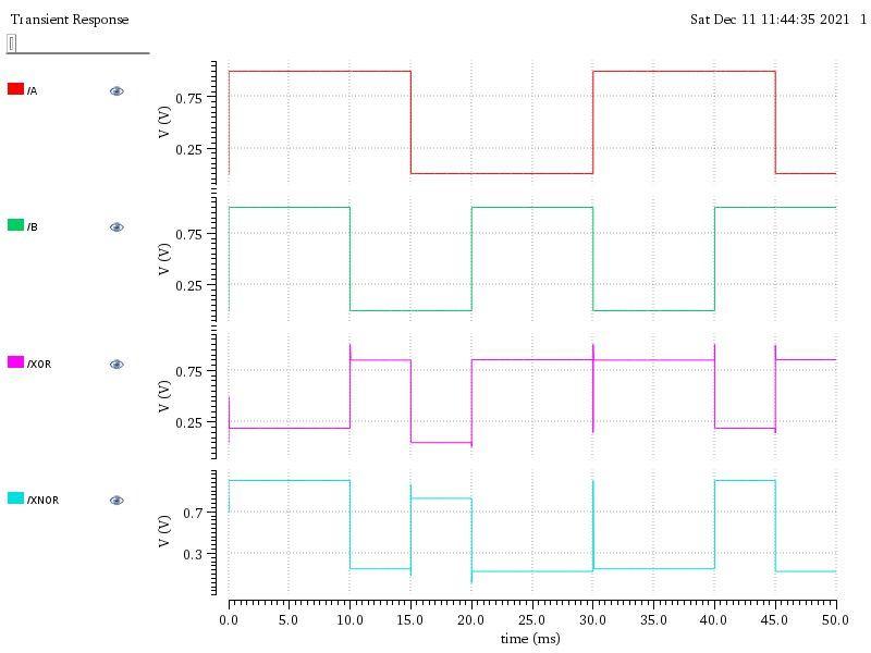
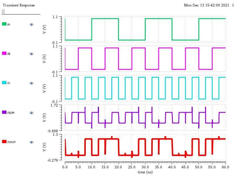
Outputs In the XOR XNOR circuit, two inputs A and B are given as pulses. After passing the inputs through the XOR XNOR and simulating through cadence virtuoso we have obtained full swing outputs which is essential for hybrid FA design.
Fig. 10 Output waveforms of XOR XNOR circuit generated by inputs A,B,C
To obtain the outputs of the Full Adder 4 we need to simulate it in a similar environment as previous full adders. We only change the number of transistors in each adder i.e., by adding inverters to reduce the consumption of power for overall circuit, but the FA 4 does use any kind of external inverters as it is constructed in CMOS logic design making use of fewer transistors. As depicted in below figure 5.5, the outputs of full adder 4 are obtained by simulating it in cadence virtuoso. In the output waveforms of FA 4, we have observed little noise.
Fig. 11. Proposed FA 4 circuit
ISSN: 2321 9653; IC Value: 45.98; SJ Impact Factor: 7.538 Volume 10 Issue X Oct 2022 Available at www.ijraset.com
We have observed that the XOR XNOR circuit that is simulated using FinFET technology shows better results in terms of power and delay. The comparison between the proposed XOR XNOR circuit and the existing circuits in terms of power consumption, worst case delay, and PDP is depicted in the following table. By comparing the proposed work with the existing circuits we have observed that the delay, power, and PDP have been reduced in the proposed model. The time delay is calculated in the cadence tool and the power is calculated through AC and DC analysis.
TABLE I. POWER,DELAYANDPDP OUTPUTSFOREXISTINGMETHODATPOWERSUPPLYOF1.2VINCMOS TECHNOLOGY
Adders with no of transistors Power(uW) Delay(ps) Power Delay Product (10 18)
Full Adder 1(20) 27.9 52.3 1459.17
Full Adder 2(26) 30.4 71.8 2182.72
Full Adder 3(26) 29.7 74.1 2200.77
Full Adder 4(20) 25.8 41.5 1070.7
TABLE II. POWER,DELAYANDPDP OUTPUTSFORPROPOSEDMETHODATPOWERSUPPLYOF1VIN FINFET TECHNOLOGY
Adders with no of transistors
Power(nW) Delay(ps) Power Delay Product (10 18)
Full Adder 1(20) 204.76 13.29 2.72
Full Adder 2(26) 317.46 37.59 11.9
Full Adder 3(26) 312.97 19 5.9
Full Adder 4(26) 201.47 12.4 2.49
ISSN: 2321 9653; IC Value: 45.98; SJ Impact Factor: 7.538 Volume 10 Issue X Oct 2022 Available at www.ijraset.com
(a) (b) (c)
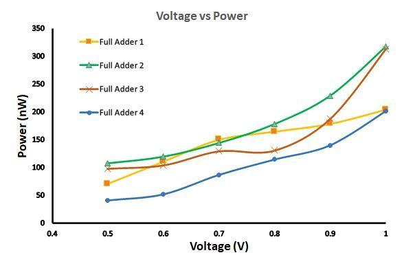
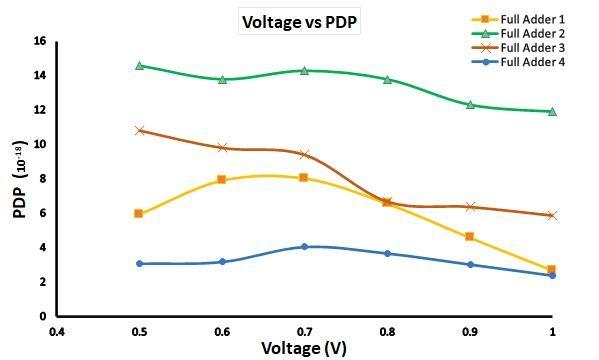
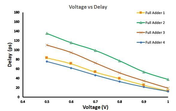
Fig. 12. (a) Delay, (b) power, and (c) PDP comparison of proposed FAs for supply voltages 0.4 1 V
In this work, a new type of full adder circuit design is presented. This full adder is designed using a hybrid logic style and a total of four FA designs are proposed. Each full adder consists of three modules for XOR XNOR output, sum, and carry respectively. An XOR XNOR circuit with ten transistors that provides full swing outputs is proposed for module 1. For modules 2 and 3 four sum circuits and carry circuits are proposed respectively. A total of four full adder circuits are proposed. The proposed full adder gives the best results in terms of power and delay and reduces the overall power delay product when compared to CMOS technology. The current work is done with FinFET 18 nm technology. Each of the full adder circuits provides an improved PDP when compared to that of the CMOS technologies.
ISSN: 2321 9653; IC Value: 45.98; SJ Impact Factor: 7.538
Volume 10 Issue X Oct 2022 Available at www.ijraset.com
In this work, a new type of full adder circuit design is presented. This full adder is designed using a hybrid logic style and a total of four FA designs are proposed. Each full adder consists of three modules for XOR XNOR output, sum, and carry respectively. An XOR XNOR circuit with ten transistors that provides full swing outputs is proposed for module 1. For modules 2 and 3 four sum circuits and carry circuits are proposed respectively. A total of four full adder circuits are proposed. The proposed full adder gives the best results in terms of power and delay and reduces the overall power delay product when compared to CMOS technology. The current work is done with FinFET 18 nm technology. Each of the full adder circuits provides an improved PDP when compared to that of the CMOS technologies.
This project shows the result in 18nm Technology but it can also be done using different specifications. The above proposed Full adders are designed using the different gates, inverters, lvt, and hvt transistors. The Full adders can be constructed or designed with advanced Technologies like CNTFET. With many other technologies, we can optimize the power, area, and delay and also minimize the number of transistors. Transistor scaling also can be varied from technology to technology. The size of the digital gadgets can be reduced by choosing the best technology. These technologies not only reduces the size of the circuits but also gives the best performances and efficient results.
[1] Vesterbacka, M., 1999, October. A 14 transistor CMOS full adder with full voltageswing nodes. In 1999 IEEE Workshop on Signal Processing Systems. SiPS 99. Design and Implementation (Cat. No. 99TH8461) (pp. 713 722). IEEE.
[2] Radhakrishnan, D., 2001. Low voltage low power CMOS full adder. IEE Proceedings Circuits, Devices and Systems, 148(1), pp.19 24.
[3] Zhang, M., Gu, J. and Chang, C.H., 2003, May. A novel hybrid pass logic with static CMOS output drive full adder cell. In Proceedings of the 2003 International Symposium on Circuits and Systems, 2003. ISCAS'03. (Vol. 5, pp. V V). IEEE.
[4] Chang, C.H., Gu, J.M. and Zhang, M., 2005. A review of 0.18 µm full adder performances for tree.
[5] Goel, S., Kumar, A. and Bayoumi, M.A., 2006. Design of robust, energy efficient full adders for deep submicrometer design using hybrid CMOS logic style. IEEE Transactions on Very Large Scale Integration (VLSI) Systems, 14(12), pp.1309 1321.
[6] Aguirre Hernandez, M. and Linares Aranda, M., 2010. CMOS full adders for energy efficient arithmetic applications. IEEE transactions on very large scale integration (VLSI) systems, 19(4), pp.718 721.
[7] Tung, C.K., Shieh, S.H. and Cheng, C.H., 2013. Low power high speed full adder for portable electronic applications. Electronics Letters, 49(17), pp.1063 1064.
[8] Bhattacharyya, P., Kundu, B., Ghosh, S., Kumar, V., and Dandapat, A., 2014. Performance analysis of a low power high speed hybrid 1 bit full adder circuit. IEEE Transactions on very large scale integration (VLSI) systems, 23(10), pp.2001 2008.
[9] Valashani, M.A. and Mirzakuchaki, S., 2016, May. A novel fast, low power, and high performance XOR XNOR cell. In the 2016 IEEE International Symposium on Circuits and Systems (ISCAS) (pp. 694 697). IEEE
[10] Naseri, H. and Timarchi, S., 2018. Low power and fast full adder by exploring new XOR and XNOR gates. IEEE transactions on very large scale integration (VLSI) systems, 26(8), pp.1481 1493