
10 IX September 2022 https://doi.org/10.22214/ijraset.2022.46861

Vijay Bhaskar Nittala
, Anisha Bomma2 , M. Ramana Reddy3
UG student, 3Assistant Professor in Department of Electronics and Communication Engineering, Chaitanya Bharathi Institute of Technology, Gandipet, Hyderabad, India.

Abstract: The digital signal processing and its classification applications on the energy constrained devices should be supported based on efficiency. Because such applications must perform highly complex computations especially complex multiplication processes while exhibiting tolerance for a large amount of noise and for computational errors too. So, comparing all the arithmetic computations, improving the energy efficiency of multiplication is critical. In this project, an energy efficient approximate 8 bit Vedic multiplier is proposed which gives a tradeoff between computational accuracy and energy consumption. The proposed architecture has reduced area compared to other multiplier architectures which process same number of bits. The reduced architecture area reduces the power consumption. Also, the Vedic technology adopted for the multiplication reducesthe delay further. But the approximate architecture output possesses a small amount of computational accuracy which is negligible for DSP applications.
Keywords: Digital Signal Processing, Energy Efficient, Vedic Multiplier, Approximate Multiplier Verilog HDL, and Simulations
For today’s electronic world embedded system and mobiles, energy consumption is a critical design problem lot of efforts have already been taken at various levels for improving the energy efficiency. Among other arithmetic operations, multiplication is the most time and power consuming operation. It becomes more significant for large operands and complex multiplication. Considering these constraints, a new approximate multiplier is proposed. This new method can provide much more energy efficiency than the truncated methods. The error rate is low because it effectively captures the noteworthylower bits. For DSP and its classification algorithm, generally one of two operands in the multiplication is stored in the memory. Here it is exploited to improve the energy efficiencyof the approximate multiplier further. Thearea can be effectively reduced bythe proposed approximate multiplier because many adders and gates can beexcluded in this method as compared to other multipliers. Within the approximate multiplier architecture, a Vedictechnologyis used for themultiplication which reducesthe delay in the multiplication. As the scale of integration keeps growing, more and more sophisticated signal processing systems are being implemented on a VLSI chip. These signal processing applications not only demand great computation capacity but also consume considerable amount of energy. While performance and Area remain to be the two major design tolls, power consumption has become a critical concern in today’s VLSI system design. The need for low power VLSI system arises from two main forces. First,with the steady growth of operating frequency and processing capacity per chip, large currents must be delivered and the heat due to large power consumption must be removed by proper cooling techniques. Second, battery life in portable electronic devices is limited. Low power design directlyleads toprolonged operation timein theseportable devices. Multiplication is a fundamental operation in most signal processing algorithms. Multipliers have large area, long latency and consume considerable power. Therefore, low power multiplier design has been an important part in low power VLSIsystem design. There has been extensive work on low power multipliers at technology,physical, circuit and logic levels. A system’s performance is generally determined by the performance of the multiplier because the multiplier is generally the slowest element in the system. Furthermore, it is generally the most area consuming. Hence, optimizing the speed and area of the multiplier is a major design issue. However, area and speed are usually conflicting constraints so that improving speed results mostly inlarger areas.
The Booth multiplication algorithm and Array multiplication algorithm are associated with high propagation time. But the fast multiplication process is defined by Vedic Mathematics. The Veda means store of knowledge. The Vedic mathematics means storage of knowledge of mathematics related to the high speed operations.
(IJRASET
ISSN: 2321 9653; IC Value: 45.98; SJ Impact Factor: 7.538
Volume 10 Issue IX Sep 2022 Available at www.ijraset.com
This Vedicmathematics provides the knowledge of varies area of mathematics like arithmetic, algebra, geometry using 16 important sutras. The method given in the Vedic math's is very simple. The Jagadguru Shankaracharya Bharati Krishna Teerthaji Maharaja has combined all concepts together and given its explanation. Out of 16 sutras the Urdhva Tiryagbhyam Vedic Sutra is very much useful multiplication operation. Present work is an effort to design and implement the multiplier using Urdhva Tiryagbhyam Vedic Sutra.
The Urdhva Tiryagbhyam sutra is based on vertical and crosswise multiplication algorithm. This sutra enables the parallel generation of intermediate products and eliminates unwanted multiplication steps. This type of multiplier takes a form of one ofthe low powers and high speed multiplier.
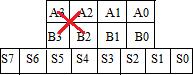
Design: Urdhva Triyagbhyam means “Vertically and Crosswise”, which is the method of multiplication followed. For the Vedic multiplication consider a 4×4 multiplier whose operands are A3A2A1A0 and B3B2B1B0.For the multiplication of a single bit a simpleANDgateisused. So, thegeneralized equations fortheoutput bitsof4X4Vedicmultiplier can be written as:
1) S0=A0B0
2) S1=A0B1+A1B0
3) S2=A0B2+A1B1+A2B0+previous carry
4) S3=A0B3+A1B2+A2B1+A3B0+previous carry
5) S4=A1B3+A2B2+A3B1+previous carry
6) S5=A2B3+A3B2+previous carry
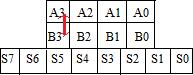
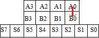
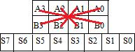
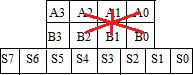
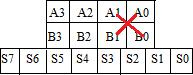
7) S6=A3B3
The S7 bit is the carry of the previous addition process. Thus, 8bit output is been obtained. The block diagram of this sutra in being referred in the Fig. 1
Fig. 1 Calculation of output bits from S0 to S7 respectively.
International
Engineering Technology (IJRASET
ISSN: 2321 9653; IC Value: 45.98; SJ Impact Factor: 7.538 Volume 10 Issue IX Sep 2022 Available at www.ijraset.com
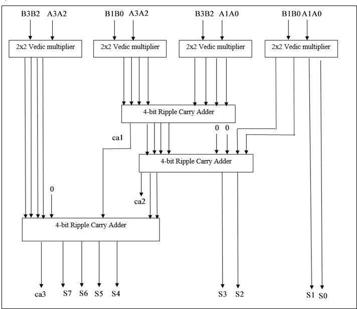
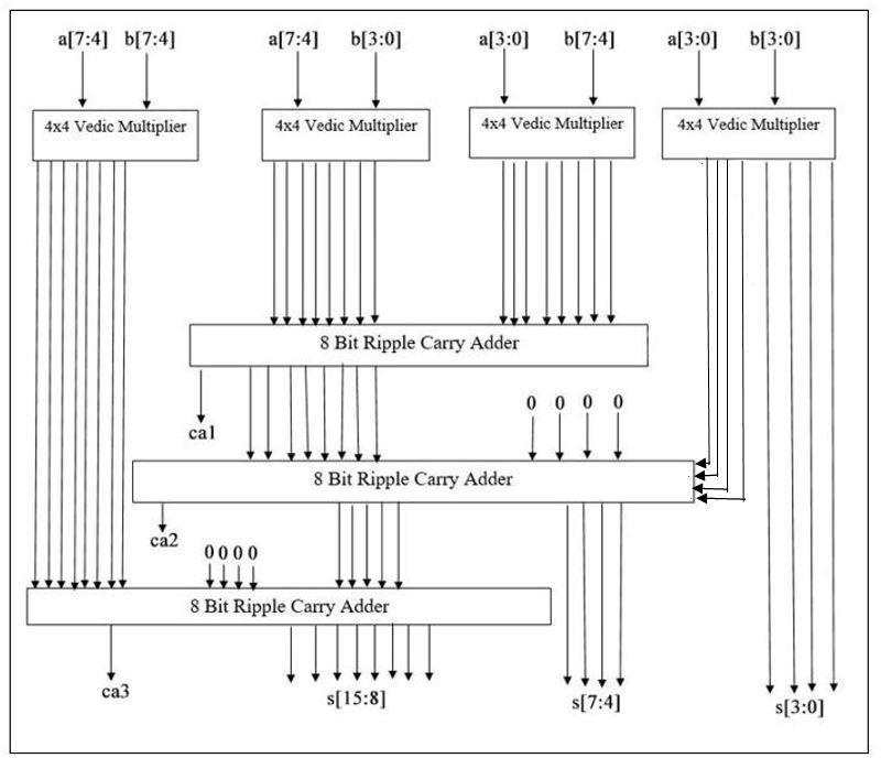
Using four 2x2 bit Vedicmultipliers and 3adders we can build 4x4 bit Vedicmultiplieras shown in Fig. 2 with proper instantiating of the 2x2 Vedic multipliers and adders. First 2x2 bit Vedic multiplier has inputs as A1A0 and B1B0. The last block is also 2x2 bit Vedic multiplier with inputs A3A2 and B3B2. The blocks in the middle are 2x2 bit multipliers with inputs A3A2 & B1B0 and A1A0 & B3B2 So, the result of multiplication will be of 8 bit as S7 S6 S5 S4 S3 S2 S1 S0 As compared to Array Multiplier, Vedic Multiplier is efficient in terms of delay and speed. The Vedic Multiplier can be used to reduce delay.
The following steps are followed in the design of the multiplier
1) Design a basic 4 bit Adder which performs the function of 4 bit addition.
2) Design an efficient 4x4 bit Vedic multiplier using half adder, full adder and 4 bit adder.
3) Design 8x8 Vedic multiplier using 4x4 bit Vedic Multiplier and 8 Bit RippleCarry Adder. 4) Design 8 bit selection architecture using 2:1 Mux and design a 3:1 Mux toperform shifting operations on output bits. 5) Energy consumption and delay of the circuit is estimated.
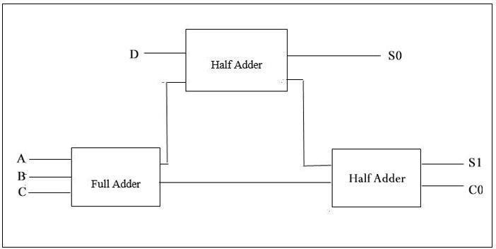
Fig. 3 A 4 bit adder is designed using half adders and full adder
Proposed 4 bit adder performs the function of 4 bit addition that gives two bits of sum and one carry as output. Its block diagram contains one full adder (FA) and two half adders (HA) as shown in the Fig.3 Here, A, B, C, D are four inputs. S0 and S1 are LSB and MSB of Sum outputs respectively and Sum is the sum of four inputs whereas C0 is the carry bit. The delay ofthe 4x4 Vedic Multiplier can be further decreased by using this proposed 4 Bit Adder.
ISSN: 2321 9653; IC Value: 45.98; SJ Impact Factor: 7.538
Volume 10 Issue IX Sep 2022 Available at www.ijraset.com
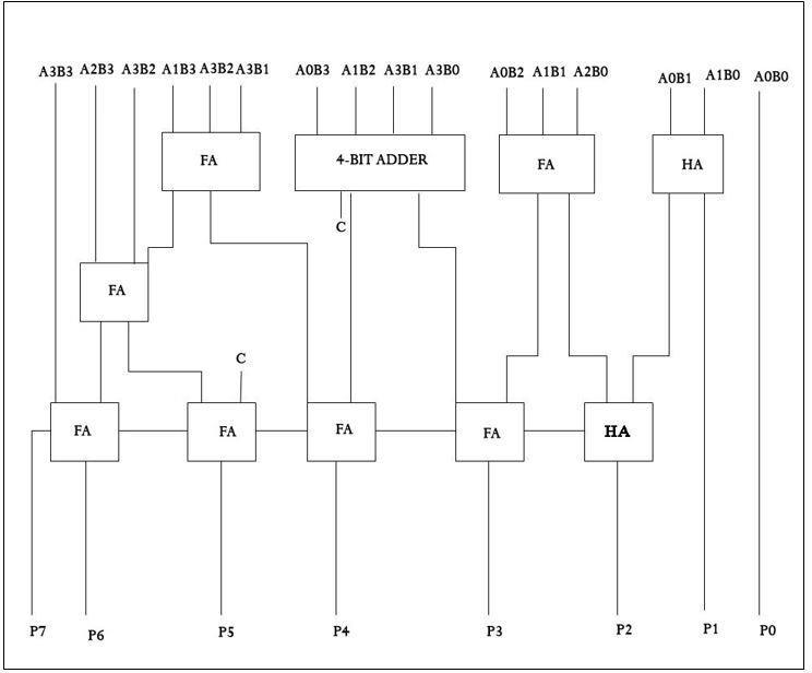
To reduce the delay, a 4x4 Vedic multiplier is implemented using half adder, full adder and the proposed 4 bit adder as shown in the Fig. 4 Here, few full adders are replaced with the half adders so that the critical path delay is reduced to a greater extent. So, the designed multiplier is much more efficient than existing Vedic multiplier. The higher bit Vedic multiplier architectures like 8 bit, 16 bit, 32 bit etc. can be built using these 4 bit Vedic multipliers. The Fig.3.2 depicts two inputs consisting of 4 bit size that results by producing an output P resulting of 8 bit size.
1) 8 bit ripple carry adder
A ripple carry adder is a logic circuit in which the carry out of each full adder is the carry in of the succeeding next most significant full adder. It is called a ripple carry adder because each carry bit gets rippled into next stage as shown in Fig. 5.
The A and B are 8 bits each.A=A0 A1 A2 A3 A4 A5 A6 A7 B=B0 B1 B2 B3 B4 B5 B6 B7
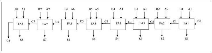
A and B are added and the corresponding sum and carry is obtained.Here, S1, S2, S3, S4, S5, S6, S7, S8 is the sum. C8 is the carry out.
Fig. 5 8 bit Ripple Carryaddder
ISSN:
9653;
www.ijraset.com
International
Science & Engineering Technology (IJRASET
ISSN: 2321 9653; IC Value: 45.98; SJ Impact Factor: 7.538 Volume 10 Issue IX Sep 2022 Available at www.ijraset.com
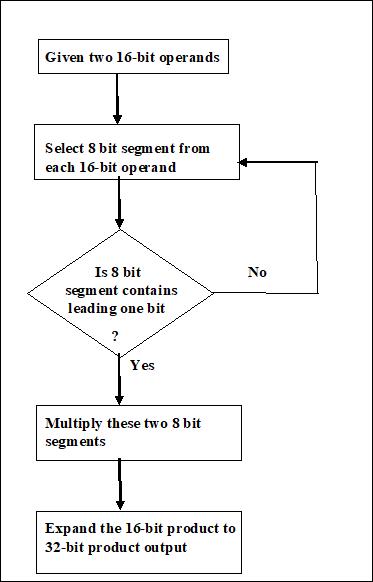
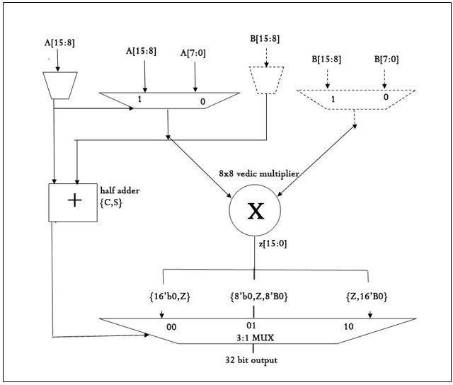
The structure of the proposed 8 Bit Selection Architecture of approximate multiplier is shown in Fig. 8. The architecture consists of two “8” bit selection units for each 16 bit operands, a multiplier unit, a 3 to 1 mux as output unit and a half adder which gives the selection bit for the output mux. Here the approximate multiplier takes only “8” consecutive bits for multiplication from each “16” bit operands. The 8 bit segment is selected only from one of two or three fixed bit positions of a positive number depending on where is its leading one bit. This technique gives a higher accuracy than simply truncating the LSBs. In this approach the 8 bit segments are selected from eachoperand from the leading one positions and it is then steered into an 8 × 8 multiplier (which is herea Vedic multiplier) and then the 2*8 output obtained from the multiplieris expanded to 2*16 output bits.
The work deals with designing Approximate multiplier with 8 bit selection architecture and which also implements Vedic multiplication. So, the outputs are considered and simulated such that required operations of multiplier are verified. To obtain the delay report of project a simulating tool name XILINX ISE SUITE 14.7 is used, whereas to obtain the power report CADENCE simulating tool is used. Once all the required building blocks are designed and verified; these blocks are integrated to design the Approximate multiplier.
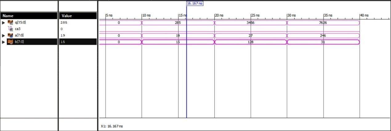
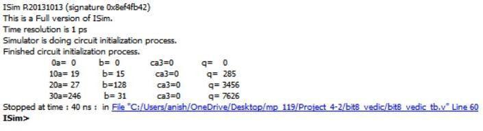
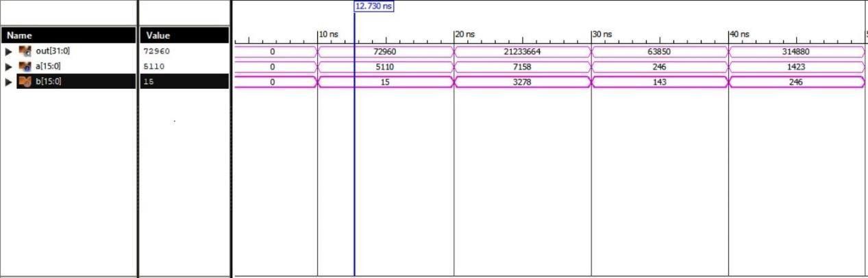
Fig. 9 Waveform of 8x8 Vedic Multiplier
From the simulation result, we can see the output of 8x8 bit Vedic multiplier for given 8 bit inputs a=19, b=15 is 285. Hence, the obtainedoutputmatches expected output.
ISSN: 2321 9653; IC Value: 45.98; SJ Impact Factor: 7.538 Volume 10 Issue IX Sep 2022 Available at www.ijraset.com
Fig. 10
approximate 8 bit
From thesimulation result, we can see theoutput of the approximate 8 bit Vedic multiplier for the given input a=5110, b=15 is 72960 whereas the expected output is 76650. Hence, approximate multiplier produces approximate output instead of exact output and sucha slighterror inoutputisnegligiblefor computation intensiveapplications which arerobust to small errors in computation.
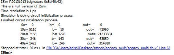
Fig. 11
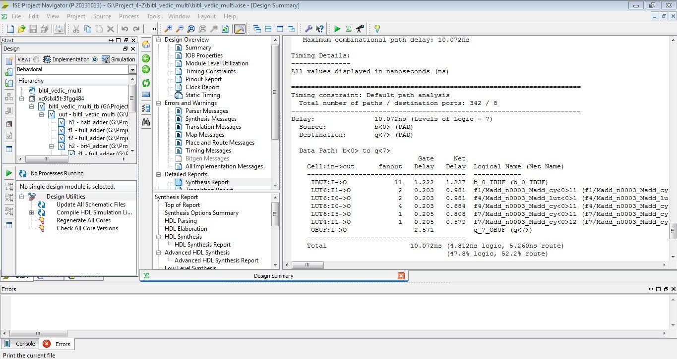
Fig. 11 shows the delay report of 4x4 Vedic Multiplier. Delay obtained for 4x4 Vedic Multiplier is 10.072 ns. Hence it can be concluded that the performance of proposed Vedic multiplier seems to be highly efficient in terms of speed when compared to conventionalmultipliers andit is evidentthattheproposed design ismoreefficientthan existing Vedic multiplier.
ISSN: 2321 9653; IC Value: 45.98; SJ Impact Factor: 7.538
10 Issue IX Sep 2022 Available at www.ijraset.com
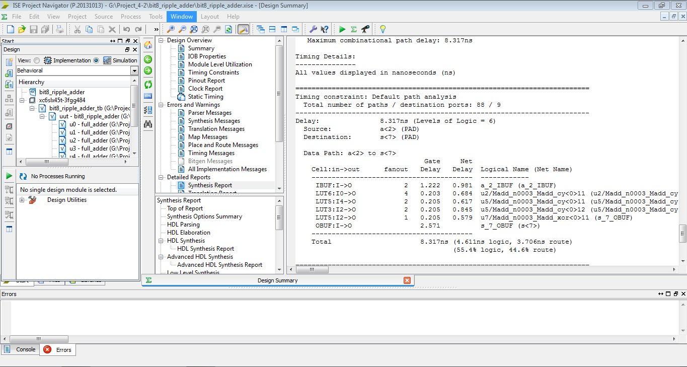
The delay report of the 8 bit Ripple Carry Adder is shown in Fig. 12 and the delay obtained is 8.317ns. In ripple carry adder, each stage of the adder must wait until the previous stage has calculated and propagates its carry signal. Therefore, the total delayof the ripple carry adder is proportional to the number of bits. Faster adders are often required for bit widths of 16 or greater.
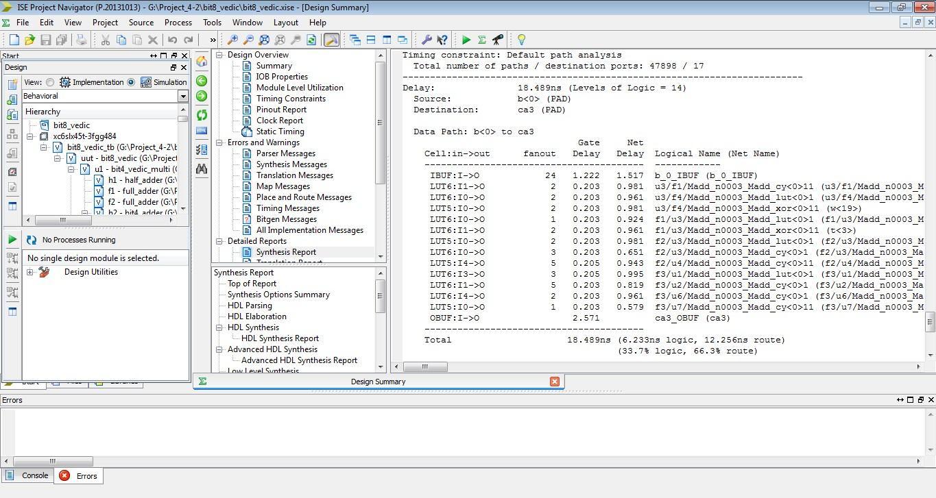
Fig. 13 shows the delay report of 8x8 Vedic Multiplier and Delay obtained is 18.489ns. Thus, proposed Vedic multiplier can be used to develop a high speed complex number multiplier with reduced delay.
ISSN: 2321 9653; IC Value:
10 Issue IX
SJ Impact Factor:

at www.ijraset.com
D.
Report
Fig. 14 Delay Report of 8 bit Vedic Multiplier
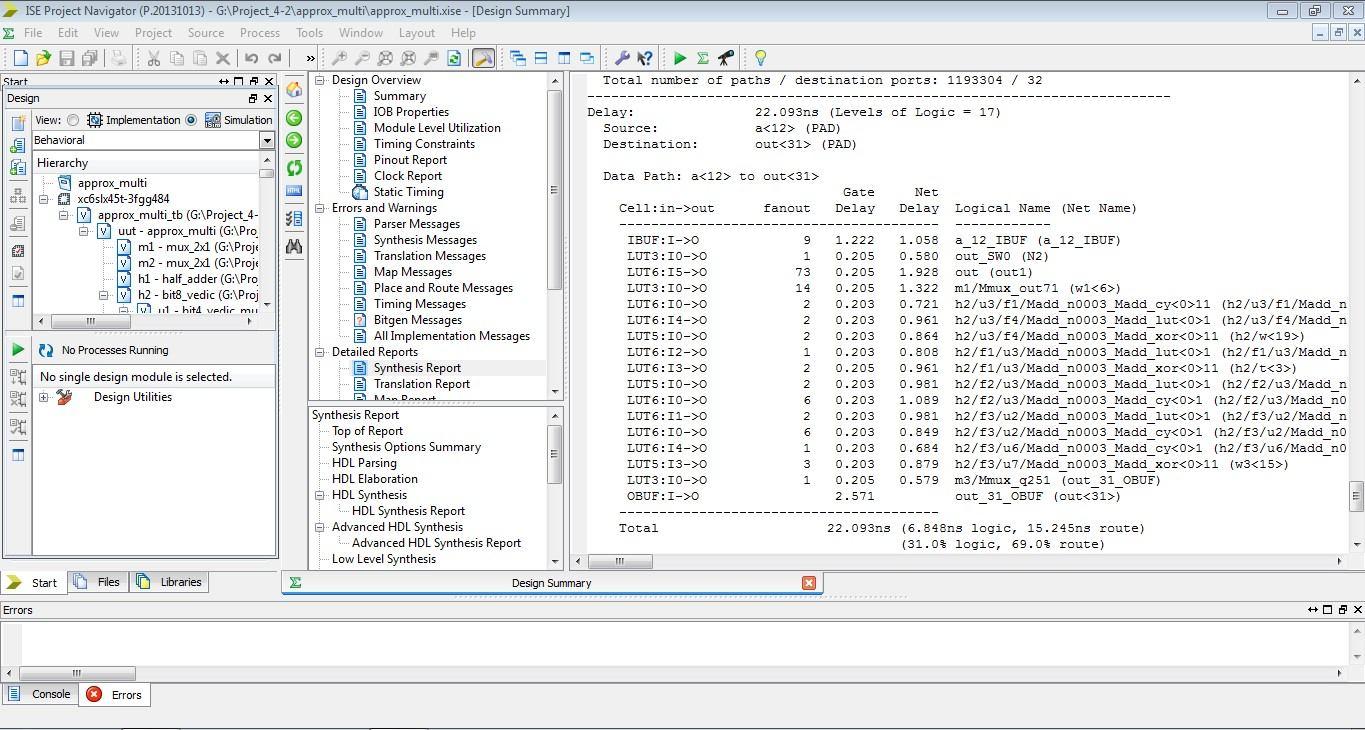
Delay obtained for the Approximate 8 bit Vedic Multiplier is 22.093ns. Thus, the bit reduction using 8 bit selection reduces the computation complexity which leads to a reduced delay and also the reduced delay Vedic architecture further reduces the delay.
E. Power Report of 4x4 Vedic Multiplier
Fig. 15 Power Report of 4x4 Vedic Multiplier
Fig. 15 shows the power report of a 4x4 Multiplier. The power consumed for 4x4 Multiplier is 0.180538mW. Here multiplication is based on Urdhva Triyakbhyam algorithm, which can reduce the power, delay, and hardware requirements for multiplication of numbers
F.
Fig.
ISSN: 2321 9653; IC Value:
10
at www.ijraset.com
8 bit Ripple Adder
Fig. 16 shows the power report of the 8 bit ripple adder. The power consumed for 8 Bit Ripple Carry Adder is 0.1121mW. The advantage of the ripple carry adder is low power consumption when compared to another adder
G. Power Report of 8x8 Vedic
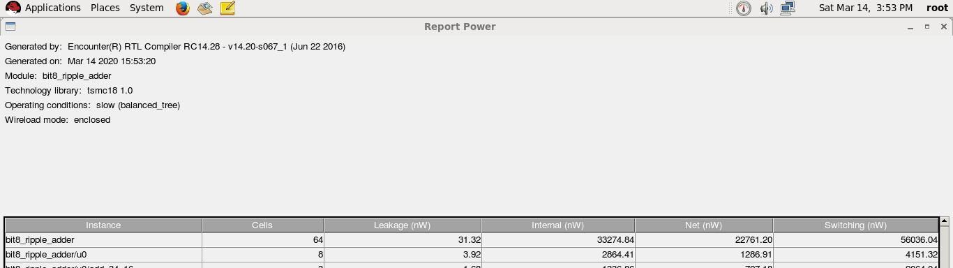
Fig.
Fig. 17 shows the report of the 8x8 Vedic Multiplier.
Report
8x8 Vedic Multiplier
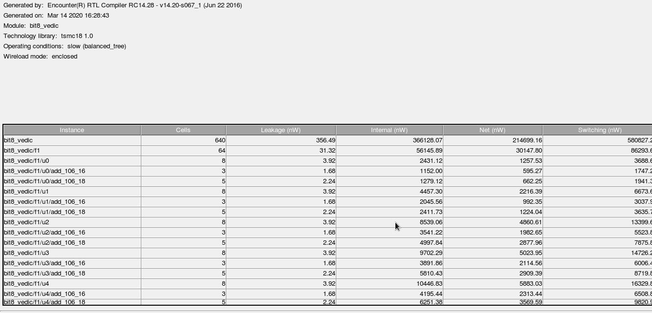
8X8 VedicMultiplier is 1.16201mW.
2321 9653;
Value:
www.ijraset.com
Power(mW)
adder 5.422 0.01368594
bit adder 5.473 0.03325859
0.18053835
8.317 0.1121034
1.16201092
6.211 0.26936871
1.53424605
0.001534
0.15687
(IJRASET
ISSN: 2321 9653; IC Value: 45.98; SJ Impact Factor: 7.538 Volume 10 Issue IX Sep 2022 Available at www.ijraset.com
Here we compare our design for the number of slices, delay, and power consumption. The data for comparison is taken from the reference paper. Thus, the proposed approximate 8 bit Vedic multiplier is more energy efficient than the other conventional multipliers. Hence the potential applications of this approximate multiplier fall mainlyin areas where there isno strictrequirement on accuracyor wheresuper lowpower consumption andhigh speedperformancearemoreimportantthan theaccuracy
Area, power consumption and increased delay are the constituent factors in VLSI design that degrades the performance of any circuit. This proposed architecture of an energy efficient multiplier in which the area, delay and power consumption are reducedto a great extent on comparing with the present works. A technique for the multiplication of 8 bit operands with the help of Vedic multiplier is described. The proposed architecture is based on “Urdhva Triyakbhyam” sutra of Vedic mathematics which is a general multiplication technique for multiplication. This algorithm makes the parallel generation of partial products and removes unwanted multiplication steps and hence results in faster multiplication. Also, with this algorithm the increase in delayand power consumption is less with the increase in number of bits. This proposed technique works in two steps. In the first step the equation for each bit of the resultant is computed. In the second step that equation is executed with the required multipliers and Ripple Carry Adders. The reduction of number of bits which takes part in multiplication reduces the complexity of the multiplication process and thus improves the efficiency. The number of, half adders and full adders used in the proposed multiplier architecture is much less than the conventional multiplier architectures. The significant reduction in the proposed architecture offers a great advantage in the reduction of area and therefore the total power consumption. Thus, the proposed 8 bit multiplier is more energy efficient than the other conventional multipliers. Also, the bitreduction using 8 bit selection reduces the computational complexity which leads to a reduced delay and also the reduced delay Vedic architecture further reduces the delay. The potential applications of this approximate Multiplier fall mainly in areas where there is no strict requirement on accuracy or where super low power consumption andhigh speed performance are more important than the accuracy. The 8 bit approximate Vedic multiplier can be used for various digital signal processing applications where complex computations are to be performed.
Future scope ofthe work includes improvingtheperformanceofthe approximate Vedic multiplier byusingEnhanced StaticSegment Method for segment basedmultiplication,to provide good accuracy at notably low energy consumption considerable reduction inarea overhead and use of carry look ahead adder in design of Vedic multiplier which inturn reduces the propagation delay by introducing more complex hardware.
[1] K. Y. Kyaw, W. L. Goh and K. S. Yeo, “Low power high speed multiplier for error tolerant application “, in IEEE Intl. Conf. Electron Devices and Solid State Circuits (EDSSC), 2010, pp. 1 4.
[2] Kaustubh Manikrao Gaikwad and Mahesh Shrikant Chavan,” Analysis of Array Multiplier and Vedic Multiplier using Xilinx", in Communications onApplied Electronics (CAE), Volume 5 No.1, May 2016.
[3] Mageshwari , G.A. Sathish Kumar,” Design and Development of Approximate Multiplier Using Urdhva Algorithm”, in International Journal of Innovative Research in ComputerandCommunicationEngineering, Vol.5, Special Issue 3, April 2017.
[4] B.Anish, Fathima, C.Vasanthanayaki,” Design and Implementation of Energy Efficient Approximate Multiplier”, International Journal of Computer Applications (0975 8887), NCICT (2015).
[5] Sumant Mukherjee,Dushyant Kumar Soni,“EnergyEfficient Multiplier forHigh Speed DSP Application”, in IJCSMC, Vol. 4, Issue. 6, June 2015.
[6] Pushpalata Verma, “Design of 4x4 bit Vedic Multiplier using EDA Tool”, in International Journal of Computer Applications (0975 888), Volume 48 No.20, June 2012
[7] “Synthesis and Simulation Design Guide” available at www.xlinx.com
[8] “Digital Design Flow” for Cadence
[9] Z. Babi´c, A. Avramovi´c, and P. Bulic, “An Iterative Logarithmic Multiplier” in 2011
ISSN: 2321 9653; IC Value: 45.98; SJ Impact Factor: 7.538 Volume 10 Issue IX Sep 2022 Available at www.ijraset.com
Dr. M. Ramana Reddy has a research experience of more than 4 years. He is working as an Assistant professor in ECE Department at Chaitanya Bharathi Institute of Technology. His educational qualification is Doctor of Philosophy in VLSI. He has published 6 research papers in international journals. His area of specialization is CMOS VLSI.


Mr. Vijay Bhaskar Nittala is a young researcher pursued Bachelor of Engineering in Electronics and Communication at Chaitanya Bharathi Institute of Technology, Hyderabad. He has been trained in System Verilog, Computer Architecture and Discrete Mathematics. He has published 2 research papers in international journals. His research areas of interest are VLSI and Computer Engineering.
Mrs. Anisha Bomma is a young researcher currently pursuing Masters of Technology in Embedded Systems at Vellore Institute of Technology, Tamil Nadu. She completed Bachelor of Engineering in Electronics and Communication at Chaitanya Bharathi Institute of Technology, Hyderabad She has been trained in System Verilog, Embedded Systems and System Engineering. Her research areas of interest are VLSI, Embedded Systems and Micro Electronics.