
ISSN: 2321 9653; IC Value: 45.98; SJ Impact Factor: 7.538 Volume 10 Issue IX Sep 2022 Available at www.ijraset.com



ISSN: 2321 9653; IC Value: 45.98; SJ Impact Factor: 7.538 Volume 10 Issue IX Sep 2022 Available at www.ijraset.com

Abstract: Nowadays Switched mode power converters are playing a significant role in the industries by providing higher efficiency for various applications. There are various applications that implement power supply and battery charge circuits for devices like smartphones, TVs, and various electronic devices When it comes to DC DC Converters the most popular among the industries are buck converters and the efficient version of the buck converter is the Synchronous buck converter. The SBC steps down the voltage from higher to lower levels. Efficiency is a crucial parameter as the industry’s focus is on delivering greater performance devices. The power converter's design must be optimized to maximize performance to achieve customer expectations. As a result, a thorough understanding of the synchronous buck converter and how to properly select the circuit components is critical. The proposed work aims at optimizing the Synchronous Buck Converter components such as Inductors, Capacitors, and Resistors. The idea of this optimization study is to improve the performance of the converter and reduce power losses and cost cutting. In this paper, the control mode considered is peak current mode control.
Keywords: Synchronous buck converter (SBC), Switch mode power supply, Optimization of design.
In recent times, Switch Mode Power Converters (SMPS) are playing a prominent role in various applications due to their high efficiency solutions. These are one of those silent (but loud electrically) gadgets that keep our electronics functioning. Despite their silence, they are the backbone of our board. DC DC converters require careful component selection to deliver power efficiently to a load in power hungry applications. SBCs are a common DC DC converter topology that provides power conversion at high efficiency while stepping down the input voltage to a lower level. Inductors for these converters are a common component selection question. SBCs are designed to limit power loss through heat and minimize ripple in the current while using an inductor and other components.
With a synchronous buck converter, the output voltage can be regulated to be lower than the input voltage, and the current can be delivered at a high rate while the power loss is minimized. In Figure 1, we can see two power MOSFETs, an output inductor, and an output capacitor making up the synchronous buck converter. The control technique of the two power MOSFETs gives rise to the name of this specific buck topology. ON/OFF states of the MOSFETs are synchronized by restraining them from turning ON at the same time and along with yielding the regulated output voltage. In the figure shown M1 and M2 are the high and low side MOSFETs respectively. When M1 is ON M2 is off and the load is supplied through the high side MOSFET. In this mode inductor current increases and in turn, charges the filter. Now in the second mode M2 is turned ON and M1 turns off and now the load is supplied through low side MOSFET. In this mode inductor, the current decreases and discharges the filter. MOSFETs here are controlled such that they don’t turn on at the same time which leads to direct short to ground.

International Journal for Research in Applied Science & Engineering Technology (IJRASET)

ISSN: 2321 9653; IC Value: 45.98; SJ Impact Factor: 7.538 Volume 10 Issue IX Sep 2022 Available at www.ijraset.com
The duty cycle of the Synchronous Buck Converter is determined by the high side MOSFET ON time
(eq.1)
For example, if the duty cycle is 0.3 then this depicts that the high side MOSFET will be ON for 30% of time and if considering the input voltage (Vin) as 30V then the output voltage produced will be 30% of Vin which is approximately 9V.
It all comes down to the converter's operating principles and how the inductor works in tandem with the other components to deliver a dependable and trouble free operation Some of the factors which greatly affect the inductor selection for a converter are 1. The rated inductance value of the inductor and how greatly it impacts the ripple current of the converter. 2. Depending on the converter’s output current requirement, DC current rating is directly in link with the rise in temperature of the inductor and the DC resistance. 3. Saturation current is typically given on all datasheets for power inductors. It is defined as the applied DC current at which the inductance value falls by a given amount below its measured value when no DC current is applied. 4. In association with the switching frequency and substance used in manufacturing the inductor the core loss also plays a significance. 5. The physical size of an inductor is proportional to the amount of energy it can store. Varying core materials may store different quantities of magnetic energy per volume, although inductor size is mostly determined by energy storage within the same core material. The mentioned considerations affect the reliability of inductors and some converters When the inductor ripple current does not recover to its starting value at the start of the following switching cycle, subharmonic oscillation develops. In peak current mode control, these oscillations occur when the duty cycle is more than 50%
(eq.2)

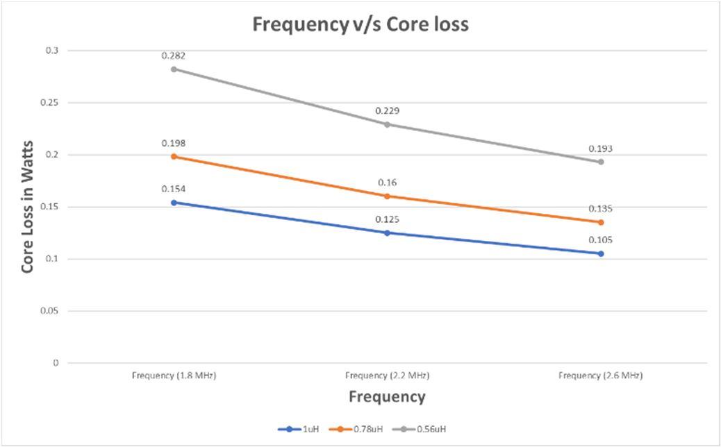
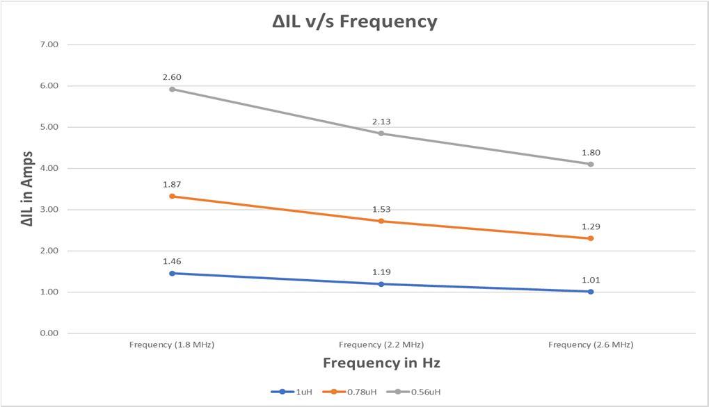
Lower the inductor value higher the peak to peak current along with small size and low cost whereas for a higher inductance value lower the peak to peak current along with a reduction in RMS and ripple current but raising the requirement of large output capacitors.
Impact Factor
Impact Factor 7.894
ISSN: 2321 9653; IC Value: 45.98; SJ Impact Factor: 7.538 Volume 10 Issue IX Sep 2022 Available at www.ijraset.com

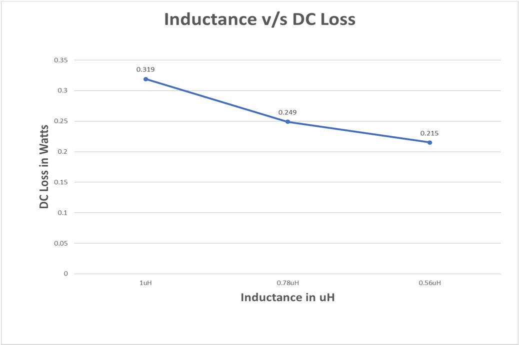
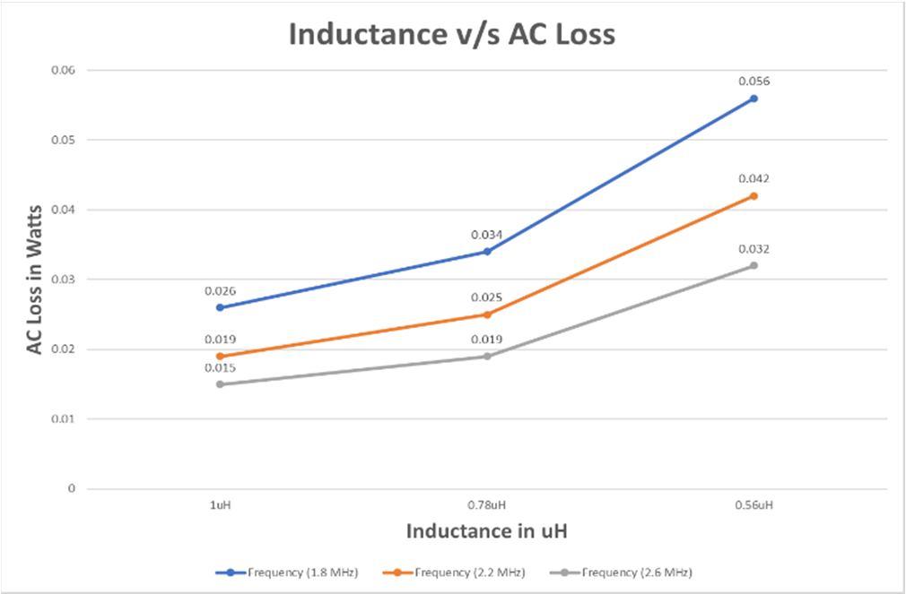


The above table depicts the comparison of three different inductance values for the same design We can see a significant decrease in the ripple current with increase the inductance value also decreasing the total power loss. Comparatively the cost of 2uH inductor is lesser than 1uH which makes is more feasible to selection.
The circuit you're dealing with, and the type of current being used are the two main factors to consider when choosing a capacitor (AC, DC, etc.). A polarised or non polarized capacitor may be required; therefore, you should decide. The amount of charge that is held in a capacitor determines its voltage. Although they pass AC, they can impede DC signals. Additionally, ripples may be removed using capacitors. A capacitor may balance the voltage if a line carrying DC electricity has ripples by absorbing the peaks and filling in the valleys. The amount of voltage to which you may expose a capacitor determines its rating rather than its voltage. For instance, if your power source is 12 volts, you should pick a capacitor with at least twice that amount of voltage, such as 25 volts, just to be cautious.

Journal for Research in Applied Science & Engineering Technology (IJRASET)

ISSN: 2321 9653; IC Value: 45.98; SJ Impact Factor: 7.538 Volume 10 Issue IX Sep 2022 Available at www.ijraset.com
The capacitor should be placed at a location that is appropriate for it. For instance, if the capacitor is linked to the battery, there is a chance that it might experience a circumstance where the voltage doubles or jumps during start up (ex. Normal voltage is 12V but due to jump start it may be subjected to 24V). As a result, the capacitor you choose must be able to handle aberrant voltage. Additionally, you must ensure that a capacitor with a working voltage higher than necessary won't grow too big and produce cross over or noise problems. Making the right capacitor selection will help you save time and money. Given that they are utilised in so many various types of electrical equipment, the sheer number of capacitors available on the market might be confusing. When choosing how to purchase capacitors for applications, it's necessary to consider their size, shape, material, and placement. We ran an optimizer (developed in house) to choose the right rated capacitor
Every resistor has a maximum power rating that is expressed in watts. This can be anything from 1/8th watt and several watts for power resistors. A first pass analysis would be performed by the engineer to check that the resistor is working within its rated value.
The formula is P=I2 R, where P is the power lost in the resistor, I is the current flowing, and R is the resistance. Unfortunately, things may become much more difficult; in order to perform exact work, the engineer needs consider the resistor's thermal derating curve. This indicates how much the maximum power dissipation above a specific temperature must be reduced by the designer. De rating frequently takes place at relatively high temperatures, so this could seem speculative, but a power circuit in an enclosed housing in a hot area can regularly surpass the cut in point, necessitating a reduction in the maximum power dissipation. It's also important to remember that power loss lowers the maximum operating voltage of a resistor. Every resistor has a Maximum Dissipated Power Rating that specifies how much power it is safe to dissipate without endangering the resistor itself. Resistors that are connected to a circuit with more power than they can handle frequently catch fire and harm the circuit. A heatsink or other cooling mechanism is necessary when a resistor is being used close to its maximum power rating.

The resistor power rating is a crucial factor to consider when choosing a resistor for a particular application. The purpose of a resistor is to prevent current from flowing across a circuit by dissipating excess power as heat. When a low wattage resistor is used in a circuit where a large power dissipation is anticipated, the resistor overheats and burns out the circuit as well. It is crucial that we select a resistor that can withstand the highest amount of power dissipated. For instance, the resistance to be selected for a circuit with 12V and 50mA of current flowing through it would be, R = V/I = 12 * 50e 3 R = 240Ω
And the power dissipated would be P = V * I = 12 * 50e 3 P = 0.6Watts or 600mWatts Hence it is ideal to choose a resistor with 240Ω resistance and 660mW rating which is available in the market. Choosing a resistor more than 660mW can increase the cost and the size.
Factor
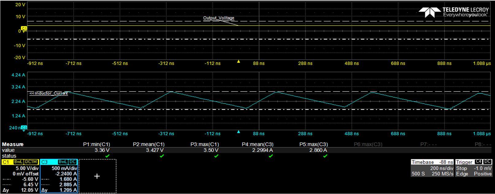
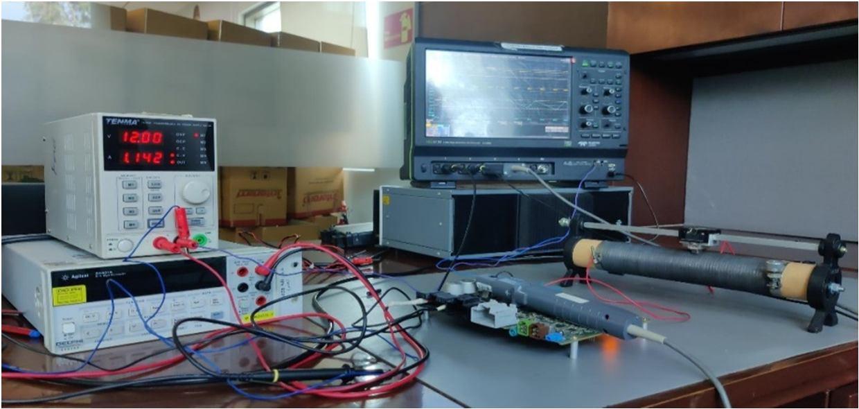


Study


International Journal for Research in Applied Science & Engineering Technology (IJRASET)

ISSN: 2321 9653; IC Value: 45.98; SJ Impact Factor: 7.538 Volume 10 Issue IX Sep 2022 Available at www.ijraset.com
[3] He Li gao and Wu Jian, "Selection of the current ripple ratio of converters and optimal design of output inductor," 2010 5th IEEE Conference on Industrial Electronics and Applications, 2010, pp. 1163 1167, doi: 10.1109/ICIEA.2010.5515878.
[4] A. Polit and A. Uramek, "Selected aspects of designing power inductors for power electronic converters," 2017 International Conference on Electromagnetic Devices and Processes in Environment Protection with Seminar Applications of Superconductors (ELMECO & AoS), 2017, pp. 1 4, doi: 10.1109/ELMECO.2017.8267713.
[5] F. H. A. Gerfer, "7 Design tips for selection of power inductors," 2016 IEEE 2nd Annual Southern Power Electronics Conference (SPEC), 2016, pp. 1 4, doi: 10.1109/SPEC.2016.7846170.
[6] E. Rachev and V. Petrov, "DC link capacitor selection for DC DC converters," 2020 12th Electrical Engineering Faculty Conference (BulEF), 2020, pp. 1 5, doi: 10.1109/BulEF51036.2020.9326085.
SJ Impact Factor 7.538 | ISRA
Impact Factor 7.894

