10 XI November 2022 https://doi.org/10.22214/ijraset.2022.47617
ISSN: 2321 9653; IC Value: 45.98; SJ Impact Factor: 7.538 Volume 10 Issue XI Nov 2022 Available at www.ijraset.com


ISSN: 2321 9653; IC Value: 45.98; SJ Impact Factor: 7.538 Volume 10 Issue XI Nov 2022 Available at www.ijraset.com
Abstract: A digital comparator is a hardware electronic device or a combinational logic circuit. It is capable of comparing two numbers as input in binary form and determines the output. In the previous designs like in the design of XOR XNOR(XE) with cross-coupled p-MOS, even though it occupies less area, the full swing output voltage can’t be able to produce which creates a problem when the bit width increases. To avoid this kind of disadvantages we are designing a N bit digital comparator in a way such that it produces full swing output voltage with the improved power efficiency as well as the transistor count in the circuit also decreases. So that it can be used in several applications like scientific computations and test circuit applications etc.

A digital comparator is a hardware electronic device that takes two numbers as input in binary form and determines whether one number is greater than, less than or equal to other number. It can be used in several applications such as IR sensors, OP amp’s, Image processing etc.
In one of the previous designs [9], an eight transistor XOR XNOR(XE) with cross coupled P MOS, is used to design the comparator and it helps in improving the speed and power efficiency. But it is not applicable in the increased bit widths because if the bit width increases it can’t be able to produce full swing output voltage.
In another design [8], it uses different logic techniques for the comparison of transistor count, power consumption and propagation delay. And to improve the propagation delay a hierarchical prefix tree structure method had been proposed [10]. However, the power consumption will be more for log2 N comparison levels for the wide input operands. Several comparator designs have also been verified like parallel prefix tree structure’s, dynamic logics, using subtractors or multipliers in the designing process etc. each having several specifications.
In the evolving VLSI technology, it is important to design any electronic component with less area and improved power efficiency and operating speed. In this paper we are designing the comparator which is efficient in terms of speed, power consumption and area. To improve the power consumption, we have used parallel prefix tree structure method, and to produce the full swing output voltage a novel EX OR NOR cell had been considered from [3].
Table 1: Used symbols and abbreviations
ALB A is less than B
AEB A is equal to B
AGB A is greater than B A Input operand B Input operand
Represents equal bit pair
Represents unequal bit pair
NOR operation
X OR operation CEM Comparison evaluation model FM Final module
ISSN: 2321 9653; IC Value: 45.98; SJ Impact Factor: 7.538
Volume 10 Issue XI Nov 2022 Available at www.ijraset.com
Let’s consider 2 input operands A and B as shown in fig.1. In the comparison process, the bits will be compared form MSB to LSB. It keeps comparing until it encounters two unequal bit pairs. If the output is equal then it means that AEB. If the output is not equal then it will check for less than or greater than. In comparing the bits from MSB to LSB the bit that first encounters logic 1 is greater than the other operand. The outputs for unequal bit pairs are AGB and ALB.
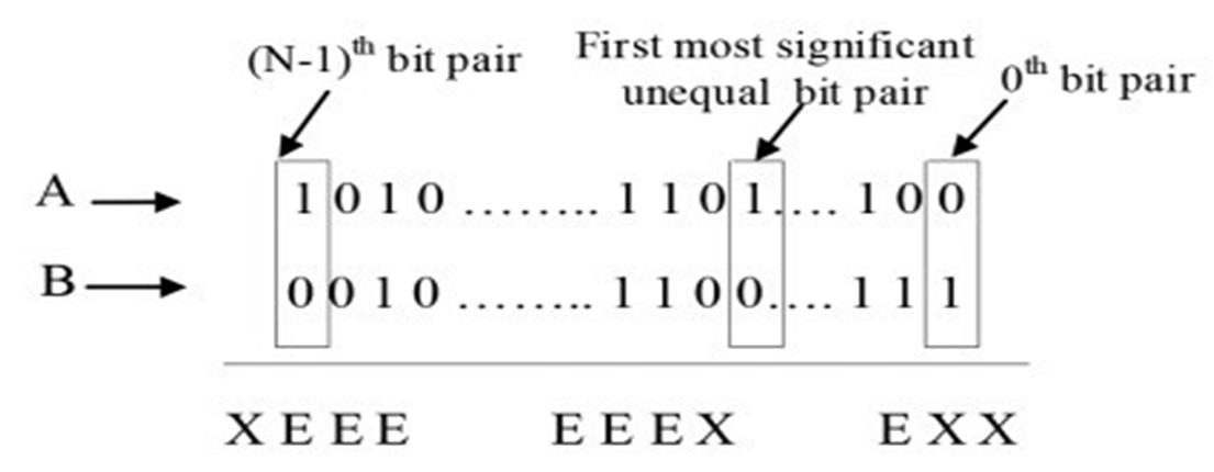
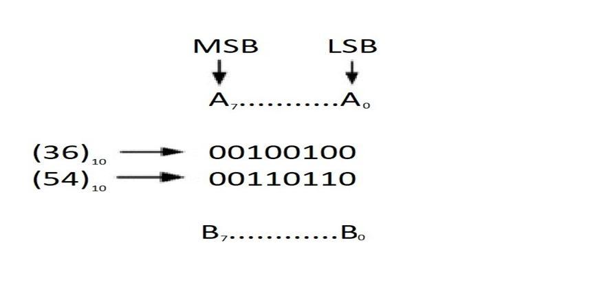
Fig 1: Comparison between two 8 bit operands
Fig 2: Comparison between two N bit operands
For the proposed N bit comparator the RTL design for a 4 bit is shown in fig.3. The circuit has been divided into two sections, they are
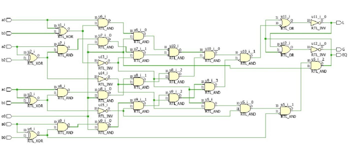
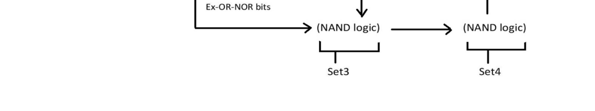
Comparison evaluation module as the name indicates all the comparison process will be done in this section. This section has its individual steps, in each step each type of operation will be performed. In step 1, the XOR and X NOR operations will be performed. In step 2, AND logic will be used and the inputs are the outputs of XNOR operation from step1 and equality pin(E). In step 3, NAND operation will be performed and the inputs for the NAND gate are the outputs of XOR operation in step1, E and input bits of the operand A. In step 4, the outputs of the NAND logic will be given as the inputs to another NAND gate. Section 2 is known as Final Module. The final result will be decided in this section. The outputs of step 2 and step 4 will be provided as the inputs to the 1st NOR logic and it decides the logic o or 1 for ALB, if ALB=0 then this output and the output of step2 will be provided as the inputs for the 2nd logic and the final result will be provided.
Fig.3: RTL design of the 4 bit comparator with reference to the proposed N bit digital comparator
ISSN: 2321 9653; IC Value: 45.98; SJ Impact Factor: 7.538 Volume 10 Issue XI Nov 2022 Available at www.ijraset.com
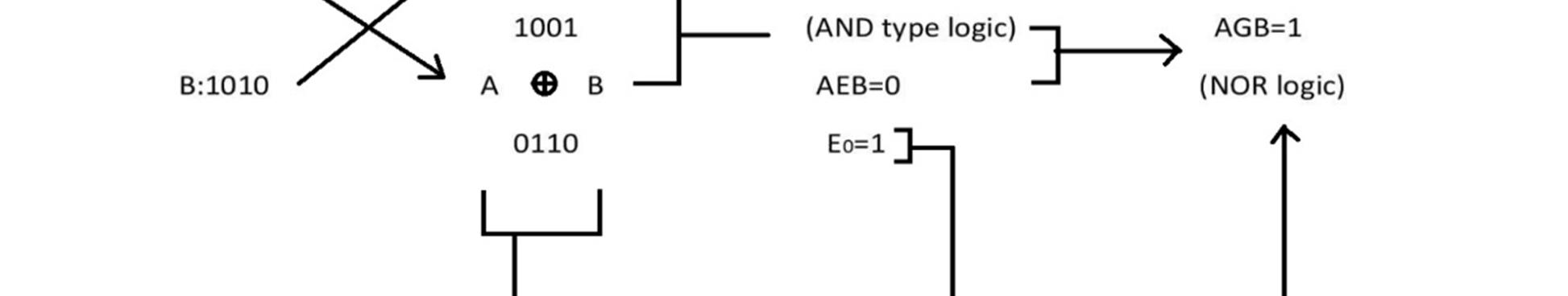
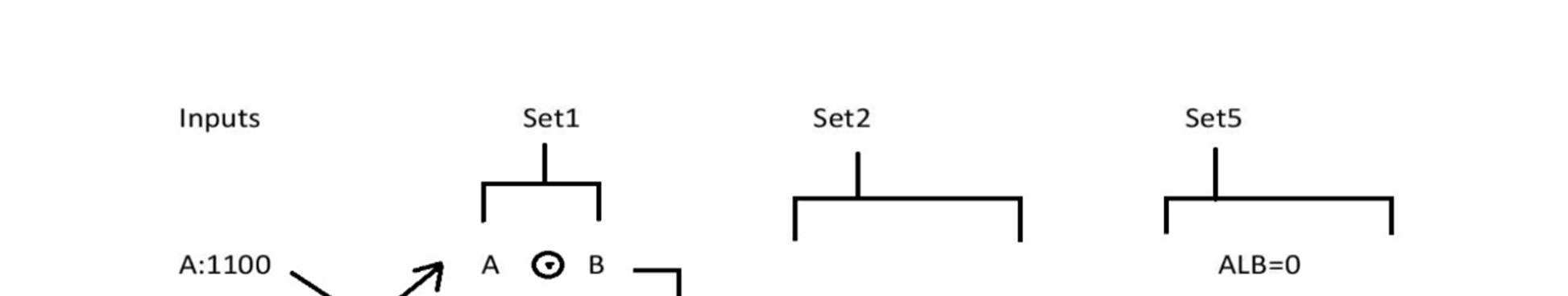
This novel EX OR NOR cell is based on pass transistor logic and CMOS logic and this logic has been considered from [3]. It consists of 7 transistors. The M5 transistor in the cell is used for producing full swing output voltage as shown in fig6. In the feedback a PMOS transistor is connected which helps in maintain the logic level on the EX NOR output terminal. The CMOS logic is used to improve the output for achieving the full swing on the EX OR output terminal. Let’s consider an example for the proposed N bit comparator. To explain the process, we have considered a two 4 bit operands A and B, where A=1100, B=1010. Set 1 compares for the equal and unequal bit pairs. The outputs of set 1 are 1001 and 0110. The output 1001 will be the input for set 2 which includes E0=1 and the output of set 2 is AEB=0. In set 3 and 4 the NAND logic will be performed with its previous sets outputs as it’s input’s. And in set 5 the final result will be obtained i.e., ALB=0and AGB=1
Fig.4: 4 bit comparison using the proposed methodology
The area is analysed by estimating the total number of cells required in each set and the logic cells will be translated into total number of transistors [3]. The total number of logic cells required in CEM and FM are
LCCEM = (N × (set 1 cell)) + (N/4 × (set 2 cell)) + (N × (set 3 cell)) + (N/4 × (set 4 cell))
LCFM = (2 × (set 5 cell))
Where N = Bit width, LCCEM = Logic cells in CEM, LCFM = Logic cells in FM
Table 2: The following table illustrates total number of transistors for different bit widths in CEM
Bit width Number of transistors in set 1
Number of transistors in set 2
Number of transistors in set 3
Number of transistors in set 4
Total Number of transistors 4 28 48 8 84 8 56 12 96 16 180 16 112 36 192 32 372 32 224 84 84 64 756 64 448 180 768 128 1524
ISSN: 2321 9653; IC Value: 45.98; SJ Impact Factor: 7.538 Volume 10 Issue XI Nov 2022 Available at www.ijraset.com
To minimise the power usage, we need to reduce the usage of no. of transistors. Mainly we have to minimise the switching activities. Hence in the proposed comparator the switching activities have been minimised using the termination bits in the computations.
The below graph compares the transistors used in the proposed comparator and different comparators
0 200 400 600 800 1000 1200 1400 1600 1800 2000
Category 1 Category 2 Category 3
Previous model Proposed model
Fig. 5: The graph compares the usage of transistors in the proposed model with the previous models
The X axis indicates Different comparator structures and the Y axis indicates Number of transistors.
The operating speed is estimated by the total delay. The total delay is the summation of the cell delays that comes across in the critical path. The total critical path delay (DCEM) in CEM can be estimated by using the following equations [3] DCEM = Dset 1 + Dset 2 + Dset 3 + Dset 4 where, Dset 1, Dset 3 and Dset 4 is equal to Du and Dset 2 is equal to (N/4) DU. Hence, the above equation can be written as DCEM = DU + (N/4) DU + DU + DU The totaldelay in FM(DFM) is estimated by DFM = 2DU Hence the total delay can be written as DT = DCEM + DFM DT = 5DU + (N/4) DU
Table 3: Delays for different bit widths of this model compared with previous models
Bit width Maximum delay(ns) for the proposed comparator Maximum delay(ns) for the previous comparators 4 0.29 0.53 8 0.31 0.62 16 0.37 0.86 32 0.47 1.12 64 0.53 1.93
ISSN: 2321 9653; IC Value: 45.98; SJ Impact Factor: 7.538 Volume 10 Issue XI Nov 2022 Available at www.ijraset.com
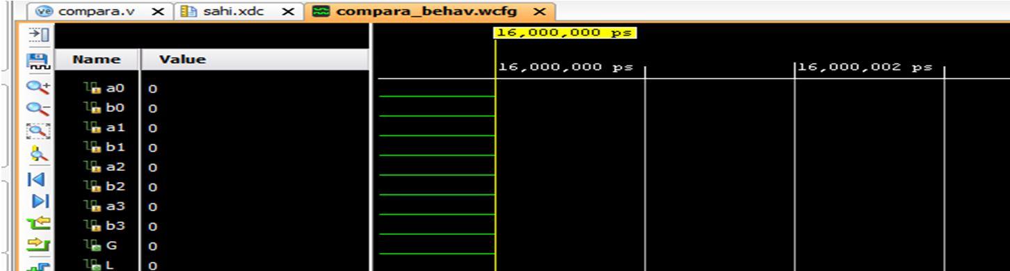
The proposed N bit digital comparator has been designed and observed for 4 bit comparison. The RTL design and the behavioral simulation results for the 4 bit are shown in the following figures. And it is observed on Zed board
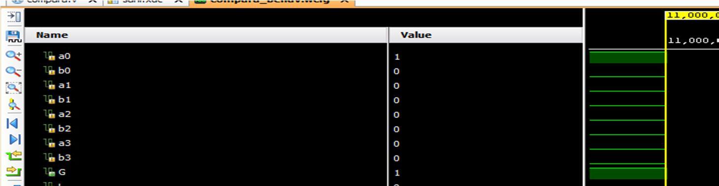
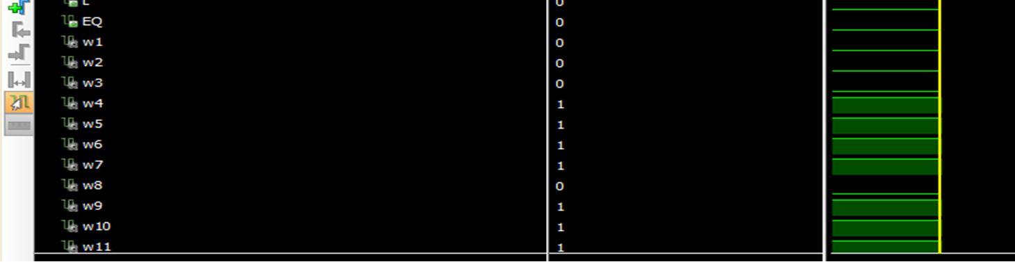
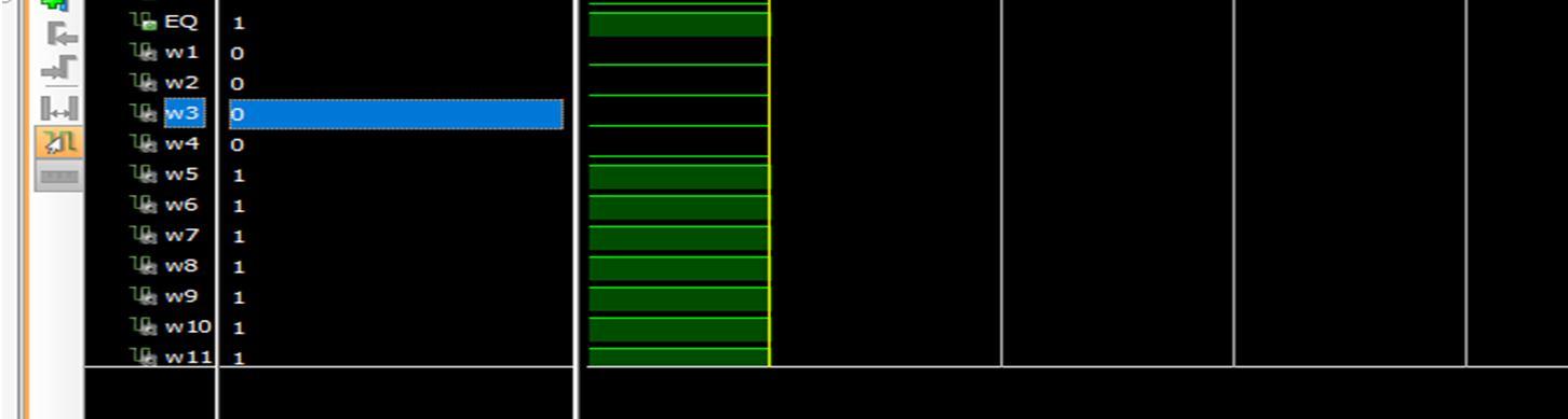
Fig. 6: Behavioural simulation of a 4 bit comparator for A=B
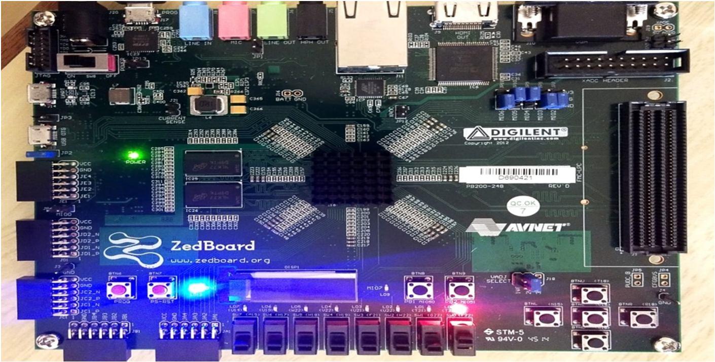
Fig 7: Behavioural simulation of a 4 bit comparator for A>B
Fig. 8: 4 bit comparison for A<B on Zed Board
ISSN: 2321 9653; IC Value: 45.98; SJ Impact Factor: 7.538 Volume 10 Issue XI Nov 2022 Available at www.ijraset.com
This paper presents a novel EX OR NOR cell which is used in implementing the proposed N bit comparator and also this novel cell is used for producing the full swing output voltage for larger bit width. The estimations for power, area and the operating speed has also been discussed. With the advantages of the proposed model, it can be used in several applications such as test circuits, memory addressing logic, scientific computations etc.
[1] Tejender Singh, Suman Lata Tripathi: “An Efficient Approach to Design a Comparator for SAR ADC”, ISBN: 978 1 6654 3802 5, July 2022.
[2] Ricardo Escobar and Ramiro Taco”, “High Speed and Low energy Dual mode Logic based Single Clack Cycle Binary Comparator”, Vol.9, ISSN:2473 4667, Pod ISSN:2330 9954, February 2021.
[3] Piyush Tyagi, Rishikesh Pandey: “High speed and area efficient scalable N bit digital comparator”, IET Circuits, Devices and Systems, ISSN: 751 858X, March 2020.
[4] Afran Sorwar, elias Ahammad Sojib, Md. Ashik Zafar Dipto, Md. MostakvTahmid Rangon”, “Design of a High Performance 2 bit Magnitude Comparator Using Hybrid Logic Style”, ISBN:978 1 7281 6852 4, July 2020.
[5] Chilaka Lydia, Dr. M. Ashok Kumar”, “Implementation of 32 bit Parallel Prefix Adders and Comparative Study for Fastest Response”, Vol. 7, ISSN:2349 5162, pp:1093 1100, July 2020.
[6] Vijay Kumar Sharma: “Optimal design for digital comparator using QA nanotechnology with energy estimation”, International Journal of Numerical Modelling: Electronic Networks, Devices and Fields, Volume34, Issue 2, October 2020.
[7] D. N. Mukherjee, S. Panda and B. Maji: “A Novel Design of 12 bit Digital Comparator Using Multiplexer for High Speed Application in 32 nm CMOS Technology”, ISSN: 0377 2063, August 2019.
[8] Dwip Narayan Mukherjee, Saradindu Panda: “Performance Evaluation of Digital Comparator using Different Logic Styles”, IETE Journal of Research, ISSN: 0377 2063, 2018.
[9] N. V. Vijaya Krishna Boppana and Saiyu Ren: “A Low Power and Area Efficient 64 bit Digital Comparator”, Journal of Circuits, systems and Computers, vol.25, No. 12, 1650148, July 2016.
[10] J. E. Stine, M.J. Schulte: “A Combined two’s complement and floating point comparator”, IEEE, ISSN: 2158 1525, July 2005.