https://doi.org/10.22214/ijraset.2023.48924

ISSN: 2321-9653; IC Value: 45.98; SJ Impact Factor: 7.538

Volume 11 Issue I Jan 2023- Available at www.ijraset.com

https://doi.org/10.22214/ijraset.2023.48924

ISSN: 2321-9653; IC Value: 45.98; SJ Impact Factor: 7.538

Volume 11 Issue I Jan 2023- Available at www.ijraset.com
RahulKumar,RajeevKumarSingh,RanjanKumar,PranavMishra Department of Electrical & Electronics Engineering, Corporate Institute of Science and Technology (CIST), Rajiv Gandhi Proudyogiki Vishwavidyalaya, Bhopal (M.P)
Abstract: In this project Interleaved Boost Converter (IBC) with modified inductor techniques is proposed. It reduces the current stress of the main circuit components, in addition to this itcan also reduces the ripple of the input current and output voltage.
In this approach, it can be faster switching, reduce the size and cost with suitable impedance matching is achieved with reduction in auxiliary circuit reactance that has contributed much increase in the overall performance. Coupled inductor in the boosting stage helpshighercurrentsharing betweentheswitches.
The overall ripple and Total harmonics distortions are reduced in this technique without sacrificing the performance and efficiency of the converter. The driving circuit can automatically detect operational conditions depending on the situation of the duty cycle whether the driving signals of the main switches are more than 50% or not and get the drivingsignal of the auxiliary switch.
Auxiliary circuit acts as support circuit to both main switches(two conditions) and reduce the total losses and improve efficiency& power factor for large loads. The operational principle, theoretical analysis, and design method of the proposed converter are presented. The entire proposed system will be tested using MATLAB/SIMULINK and the simulation results are also present.
The interleaved boost converter design involves the selection of the inductors, the input and output capacitors, the power switches and theoutputdiodes.Boththe inductorsanddiodesshouldbeidenticalinbothchannelsofaninterleaveddesign.Inorderto select these components, it isnecessary to know theduty cycle range and peak currents. Since the output power is channeledthrough two power paths, a good starting point is to design the power path componentsusing half the output power. Basically, the design starts with a single boost converter operating at half the power. However, a trade-off exists that will depend on the goals of the design. The designer may use smaller components since currents are smaller in each phase. Or, larger components may be selected to minimizelosses.
Specifically, this design uses the criteria of room temperature operation over the entire input voltage range without the requirement of airflow. Obviously, there are many trade-offs possible, such as requiring external airflow that would allow the use of smaller componentsandmorepowerperwatt.
Inthisminorprojectwehave achievedthetwomainobjectiveswhichareasfollows:-
1) Simulationofinterleavedboostconverter.
2) Comparativeanalysisbetweenboostconverterandinterleavedboostconverter.
The Interleaved Boost Converter (IBC) consists of two boost converters connected in parallel with a 180° phase delay, and operating at the same frequency. The IBC has better characteristics when compared to a boost converter with improved efficiency, reducedsize,greaterreliability and lowerTotalHarmonicDistortions(THD).Thegatingpulsesofthetwoswitchesintheconverter areshiftedbyaphasedifferenceof360/nwherenisthenumberofparallelboostconverters.
The converter considered is operating in Continuous Conduction Mode (CCM) which results in lower input peak current (amplitude)andlessconductionlosses.Itoperatesatlargerduty cyclesay0.5due tohighoutputvoltageand lowinputvoltage.The input current for the IBC is the sum of each inductor currents and as the two devices are phase shifted by 180°, the input current ripplesaresmall.
ISSN: 2321-9653; IC Value: 45.98; SJ Impact Factor: 7.538

Volume 11 Issue I Jan 2023- Available at www.ijraset.com
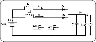
TheproposedinterleavedboostconverterisasshowninFigure1.1
The input is an unregulated DC voltage, which is obtained by rectifying line voltage. DC-DC converters are switched mode DC to DC converter and are used to convert unregulated DC input to controlled DC output. The IBC consists of two boost convertersin parallel with a phase delayof180° operating in CCM mode.The converter usestwo MOSFET switches, two inductors,two diodes, onecapacitorandaresistiveload.
Someimportantpointrelatedtointerleavedboostconverterareasfollows:-
1) The interleaved boost converter means parallel connection of converters, by parallel connection the current divided. So, the I^2Rlossesminimizedandcurrentstressdecreased.
2) Thecurrentrippleattheoutputsidewillbereduced,andthisshallreflecttheinputcurrentalso.
3) Theratingoftheconverterincreaseandtheoverallefficiencyalsoincreasesduetotheabovereasons.
4) Interleavingtechniqueisavariousswitchinginterconnectionthatimprovessynchronizingoftheeffectivepulsefrequency.
5) Theenergycanberescuedandenhancespowerconversionwithoutaffectingconversionefficiencybyaninterleavingtechnique
6) Theinterleavedboostconvertercomprisestwoparallelswitches;S1,S2 inductorsL1,L2;diodesD1,D2;CapacitorCandload resistor R with a trustworthy source of input (Vin).Phase-shifted switchingfunction controls theswitches. Theboostconverter interleavedcan operate in four modes. Only continual current mode (CCM) is analyzed in this paper in order to simplify the calculation .The two inductance values are considered similar (L1=L2=L) and similar dutycycles (D1=D2=D) with time delay byT/2.
7) A basic boost converter converts a DC voltage to a higher DC voltage. Interleaving adds additional benefits such as reduced ripple currents in both the input and output circuits. Higher efficiency is realized by splitting the output current into two paths, substantiallyreducingI2RlossesandinductorAClosses.
Aboost converteris one of the simplest types of switch mode converter. As the namesuggests, it takesan input voltageand boostsorincreasesit.
Allitconsistsofisaninductor,asemiconductorswitch(thesedaysit’sa MOSFET, since youcangetreallyniceonesthesedays),a diodeandacapacitor.Alsoneededisasourceofaperiodicsquarewave.
ISSN: 2321-9653; IC Value: 45.98; SJ Impact Factor: 7.538

Volume 11 Issue I Jan 2023- Available at www.ijraset.com
As we can see, there are only a few parts required to make a boost converter. It is less cumbersome than an AC transformer or inductor.
They’re so simple because they were originally developed in the 1960s to power the electronics systems on aircraft. It was a requirementthattheseconvertersbeascompactandasefficientaspossible.
The biggest advantageboost convertersoffer istheirhigh efficiency – someofthemcan evengoup to 99%. In other words, 99%of theinputenergyisconvertedtousefuloutputenergy,only1%iswasted.
DC-DC converters are also known as Choppers. Here we will have a look at the Step Up Chopper or Boost converter which increasestheinputDCvoltagetoaspecifiedDCoutputvoltage.

The input voltage source is connected to an inductor. The solid-state device which operates asa switch is connected across the source The second switch used is a diode. The diode is connected to a capacitor ,and the load and the two are connected in parallel asshowninthefigureabove.
Theinductor connectedto inputsourceleadsto aconstantinputcurrent,andthustheBoostconverteris seenastheconstantcurrent inputsource.
And the load can be seen as a constant voltage source. The controlled switch is turned on and off by using Pulse Width Modulation(PWM).
PWM can be time-based or frequency based Frequency-based modulation has disadvantages like a wide range of frequencies to achieve the desired controlofthe switch which in turn will give the desired outputvoltage. Time-based Modulation ismostly used forDC-DCconverters.
It is simple to construct and use. The frequency remains constant in this type of PWM modulation. The Boost converter has two modesofoperation.Thefirstmodeiswhentheswitchisonandconducting.
©IJRASET:AllRightsareReserved|SJImpactFactor7.538|ISRAJournalImpactFactor7.894|
ISSN: 2321-9653; IC Value: 45.98; SJ Impact Factor: 7.538

Volume 11 Issue I Jan 2023- Available at www.ijraset.com
A. Proposed Topology
1) Proposed IBC
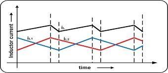
ThecircuitdiagramandtheidealwaveformsofthecurrentsintheinductorsL1andL2forinterleavedboostconverteroperatinga TccmareshowninFigures2.1and2.2.
B. Modes Of Operation
The mode of operation can be analyzed based on one channel. Since both power channels share current and because both inductors are identical, each power channel behaves identically. Based on the amount of energy that is delivered to the load during each switching period,theboostconvertercanbeclassifiedintocontinuousordiscontinuousconductionmode.Ifalltheenergystoredin the inductor is delivered to the load during each switching cycle, the mode of operation is classified as discontinuous conduction mode (DCM). In this mode the inductor current ramps down to zero during the switch off-time. If only part of the energy is deliveredtotheload,thentheconverterissaidtobeoperatingincontinuousconductionmode(CCM).
The modeof operation is a fundamental factor indetermining the electrical characteristicsof the converter.The characteristicsvary significantlyfromonemodetotheother.
1) Mode-1: During mode1 the switches Q1 and Q2 are switched on and the diodes D1 and D2are under off condition. Figure:2.3 showstheequivalentcircuitforthismode.
©IJRASET:AllRightsareReserved|SJImpactFactor7.538|ISRAJournalImpactFactor7.894|

ISSN: 2321-9653; IC Value: 45.98; SJ Impact Factor: 7.538

Volume 11 Issue I Jan 2023- Available at www.ijraset.com
2) Mode 2:- Duringmode2,theswitchQ1isinonconditionandswitchQ2isinoffconditionandD1isinoffconditionandD2 isinonconditionrespectively.Thefigure2.4representstheoperationundermode2.
3) Mode:-3 Inmode 3, theswitch Q1isin off condition and the switch Q2 is in onconditionand thecorrespondingdiodessuch as D1andD2areinonandoffconditionsrespectively.Thefigure:2.5representstheoperationofIBCundermode3.


©IJRASET:AllRightsareReserved|SJImpactFactor7.538|ISRAJournalImpactFactor7.894|

ISSN: 2321-9653; IC Value: 45.98; SJ Impact Factor: 7.538

Volume 11 Issue I Jan 2023- Available at www.ijraset.com
Both modes of operation have advantages and disadvantages. The main disadvantages in using CCM is the inherent stability problemscausedbytheright-half-planezeroin thetransferfunction.However,theswitchandoutputdiodepeakcurrentsarelarger whentheconverterisoperatingintheDCMmode.Largerpeakcurrentsnecessitate using largercurrentandpower dissipationrated switchesanddiodes.Also,thelargerpeakcurrentscausegreaterEMI/RFIproblems.MostmoderndesignsuseCCMbecausehigher powerdensitiesarepossible.Forthesereasons,thisdesignisbasedoncontinuousconductionmode.
The interleaved boost converter design involves the selection of the inductors, the input and output capacitors, the power switches and theoutputdiodes.Boththe inductorsanddiodesshouldbeidenticalinbothchannelsofaninterleaveddesign.Inorderto select these components, it isnecessary to know theduty cycle range and peak currents. Since the output power is channeledthrough two power paths, a good starting point is to design the power path componentsusing half the output power. Basically, the design starts with a single boost converter operating at half the power. However, a trade-off exists that will depend on the goals of the design. The designer may use smaller components since currents are smaller in each phase. Or, larger components may be selected to minimizelosses.Specifically, thisdesignusesthecriteria of roomtemperatureoperationovertheentireinputvoltagerange without the requirement of airflow. Obviously, there are many trade-offs possible, such as requiring external airflow that would allow the use of smaller components and more power per watt. Knowing the maximum and minimum input voltages, the output voltage, and the voltage drops across the output diode and switch, the maximum and minimum duty cycles arecalculated. Next, the average inductor current can be estimated from the load current and dutycycle. Assuming the peak-to-peak inductor current ripple to be a certain percentage of the average inductor current, thepeakinductor current can be estimated. The inductor value is then calculated using the ripple current, switching frequency, input voltage, and duty cycle information. Finally, the boundary between CCM and DCMisdeterminedwhichwilldeterminetheminimumloadcurrent.Oncetheinductorvaluehasbeenchosenandthepeakcurrents have been calculated, the other components may be selected. Selection of the input and output capacitors differ from a single phase designbecauseofthereducedrippleandincreasedeffectivefrequency.
1)
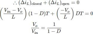
The boosting ratio of the IBC is a function of the duty ratio. It is same as in conventionalboostconverter.Itisdefinedas; V(o)/V(in)=1/(1-D)
Where,Voistheoutputvoltage,VinistheinputVoltageandDisthedutyratio.
In the power electronic systems the magnetic components play a major role for energy storage and filtering. As discussed in the operation of IBC the inductor is used to transform the energy from the input voltage to the inductor current and to convert it back fromthe inductorcurrent totheoutput voltage.Asperthe principle thetwo inductorsare identicalin ordertobalancethecurrent in thetwoboostconverters.
The first step to calculate the switch current is to determine the duty cycle, D, for the minimum input voltage. The minimum input voltageisusedbecausethisleadstothemaximumswitchcurrent.
D=1-(Vin*efficiency)/Vout
Theefficiencyisadded totheduty cyclecalculation,becausetheconverterhastodeliveralsotheenergy dissipated.Thiscalculation givesamorerealisticdutycyclethanjusttheequationwithouttheefficiencyfactor.
TheoutputcurrentismeasuredbyusingthebelowformulaIout=Pout/VoutWhere; Pout=OutputPower & Vout=OutputVoltage
ISSN: 2321-9653; IC Value: 45.98; SJ Impact Factor: 7.538

Volume 11 Issue I Jan 2023- Available at www.ijraset.com

1) STEP – 1
Tobegin with,weneedathoroughunderstandingofwhatourloadrequires.Itishighly recommended(fromexperience) thatif you attempt to build a boost converter at the beginning it is very important to know the output voltage and current independently, the productofwhichisouroutputpower.
2) STEP – 2
Once we have the output power, we can divide that by the input voltage (which should alsobedecided)togettheaverageinput currentneeded.
We increase the input current by 40% to account for ripple. This new value is the peak inputcurrent. Also the minimum input current is 0.8 times the average input current, so multiply theaverageinputcurrentby0.8. Nowthatwehavepeak and minimumcurrent, wecancalculatethe totalchange incurrentbysubtractingthepeak and minimum current.
3) STEP – 3
Now we calculate the duty cycle of the converter, i.e. the ratio of the on and off times of theoscillator. Dutycycleisgivenbythistextbookformula: D.C.=(Vout–Vin)/(Vout)
Thisshouldgiveusareasonabledecimalvalue,above0butbelow0.999.
Nowitistimetodecideuponthefrequencyoftheoscillator.Thishasbeenincludedasaseparatestepbecausethesignalsourcecan be anything from a 555 timer (where the frequency and duty cycle are completely under your control) or a fixed frequency PWM controller.
Once the frequency is determined, we can find out the total time period by taking an inverse.Now the time period is multiplied by thedutycyclevaluetogettheontime.
Sincewehavedeterminedtheontime,inputvoltageandchangeincurrent,wecanplugthosevaluesintotheinductorformula whichhasbeenrearrangedalittle: L=(V*dt)/dI
WhereVistheinputvoltage,dtistheontimeanddIisthechangein current.
1) Mode I: Switch is ON, Diode is OFF.

ISSN: 2321-9653; IC Value: 45.98; SJ Impact Factor: 7.538
Volume 11 Issue I Jan 2023- Available at www.ijraset.com
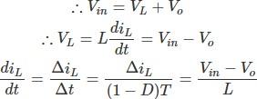
TheSwitchisONandthereforerepresentsashortcircuitideallyofferingzero resistancetotheflowofcurrentsowhentheswitchis ONallthecurrentwillflowthroughtheswitch and back to the DC input source. Let us say the switch is on for a time TON andis offforatimeTOFF.Wedefinethetimeperiod,T,asandtheswitchingfrequency, Fswitching=1/TLetusnowdefineanotherterm,thedutycycle, D=Ton/T LetusanalyzetheBoostconverterinsteadystateoperationforthismodeusing KVL, Vin=VL
VL =L(diL /dt)=VindiL / dt=Vin/L SincetheswitchisclosedforatimeTON=DTwecansaythat Δt=DT.
2)
In this mode, the polarity of the inductor is reversed. The energy stored in the inductor is released and is ultimately dissipated in the load resistance, and this helpsto maintainthe flowofcurrentin thesamedirectionthroughtheloadandalsostep-up the output voltage as the inductor is now also acting as a source in conjunction with the input source. But for analysis, we keep the original conventionstoanalyzethecircuitusingKVL.
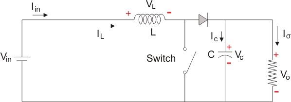
LetusnowanalysetheBoostconverterinsteadystateoperationforModeIIusingKVL.
Sincetheswitchisopenforatime
Wecansaythat;
Itisalreadyestablishedthatthenetchangeoftheinductorcurrentoveranyonecompletecycleiszero
©IJRASET:AllRightsareReserved|SJImpactFactor7.538|ISRAJournalImpactFactor7.894|
ISSN: 2321-9653; IC Value: 45.98; SJ Impact Factor: 7.538

Volume 11 Issue I Jan 2023- Available at www.ijraset.com
A. Simulation of Interleaved Boost Converter
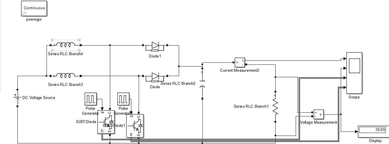
Thetwophaseinterleavedboostconverterisshownhere.Thephasedifferencebetweenthesetwopowerstageswillbe 180degree. Its simulationisshowninthenextslide.
Tofindthephasedifferencebetweenthepowerstageswehavetheformula360/n . Where‘n’isthenumberofpowerstages.Sincewearedealingwithtwostagesthereforethephasedifferencebetweenthemwillbe 180degree.
ThevalueoftheparametersconsideredinthesimulationofinterleavedboostconverterisshowninTableT-1.
©IJRASET:AllRightsareReserved|SJImpactFactor7.538|ISRAJournalImpactFactor7.894|
ISSN: 2321-9653; IC Value: 45.98; SJ Impact Factor: 7.538

Volume 11 Issue I Jan 2023- Available at www.ijraset.com
Using MATLAB/SIMULINK the simulation of interleaved boost converter is performed. Thewaveforms of the input voltage, outputvoltage,inductorcurrents,andvoltagerippleareshown.
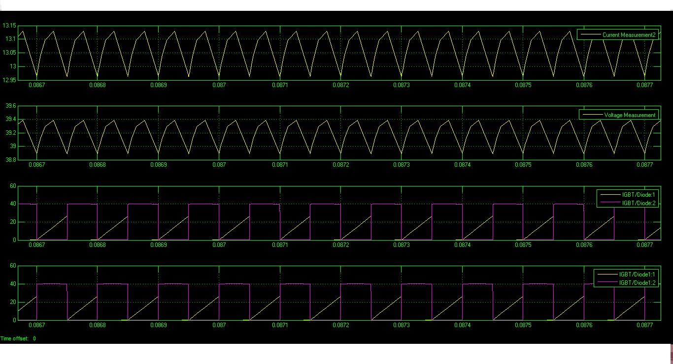
An interleaved boost dc-dc converter system has been modeled using MATLAB SIMULINK. A comprehensive simulation was conductedtoverifytheperformanceofinterleavedboostdc-dcconvertersystem.
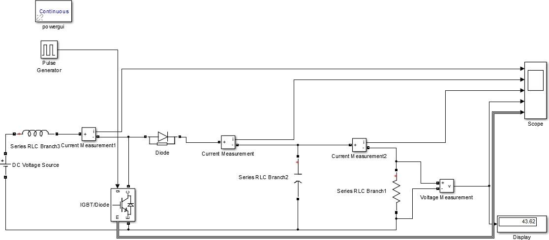
The model parameters are listed in Table T-1. The simulation waveform of interleaved boostdc-dc converter are also obtained in MATLAB.
Firstgraphrepresentsthesumofcurrentcomingoutfromthetwopowerstages.Secondgraphrepresentsthevoltage; Herewecanseethattherippleinvoltageispresentanditvaryfrom38.9to39.4.Itmeansripplepresentinvoltageis,0.5whichis veryless.ThispapermainlyfocusesonthecomparisonoftwointerleavedDCconvertertopologiesofConventionalboostconverter (CBC)usingMATLAB/SIMULINKsoftwareundersamedesignspecificationsanddutycycle.
Boost converter is a DC-to-DC converter that steps up voltage from its input to its output. This unique capability is achieved by storingenergyinaninductorandreleasingittotheloadatahighervoltage.

ISSN: 2321-9653; IC Value: 45.98; SJ Impact Factor: 7.538
Volume 11 Issue I Jan 2023- Available at www.ijraset.com
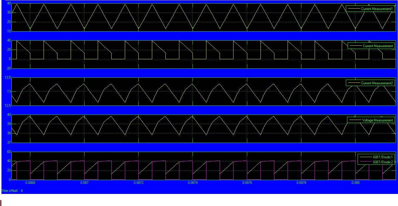
Based on the proposed design, Matlab/simulink software is used to simulate the boost converter’s performance. The simulation results of the boost converter with different values of input voltage and duty cycle are shown with respect to both mode of operationwithoutfeedbackandwithfeedback.
From the simulation results, the proposed converter is capable of providing a constant DC output voltage. The transient response doesexistsforafewmillisecondsbeforesettlestoasteadystate.
F. Parameters Considered
ThevalueoftheparametersconsideredinthesimulationisshowninTableT-2.
©IJRASET:AllRightsareReserved|SJImpactFactor7.538|ISRAJournalImpactFactor7.894|
ISSN: 2321-9653; IC Value: 45.98; SJ Impact Factor: 7.538

Volume 11 Issue I Jan 2023- Available at www.ijraset.com
Incaseofboostconverter;theripplepresentinvoltageis; 37.8to39.8
itmeansripplepresentinvoltageis
=39.8-37.8
=2ripple
So from the simulation of these two converter we conclude that in case of interleaved boostconvertertherippleinvoltagehas beenreducedincomparisontosimpleboostconverter.
Thereforeinterleavedboostconverterisbetterinoperationincomparisontoboostconverter.
1) Theadvantagesofinterleavedboostconvertercomparedtotheclassicalboostconverterare:-
a) Lowinputcurrentripple,2]highefficiency,
b) Fastertransientresponse,
c) Reducedelectromagneticemissionand5]improvedreliability.
2) The interleavedboostconverter improveslow – voltagesstressacrossthe switches, low input currentripple also improving the efficiencycomparedwithatraditionalboostconverter.
3) To validate the performance in terms of input and output ripple and values, the two converters were tested using MATLAB/SIMULINK.
The use of applications driven by batteries improves the demand for effective dc-dc converters during modern day-to-day life. These include a wide range of solar based applications, Fuel cell systems, uninterrupted power supplies (UPS) and hybrid electric vehicles. Boost converters are the suitable converters among the DC to DC converters to charge the batteriesdue to their capability of boosting up the voltage since low level to high level. But conventional boost converters suffer from high ripple content in the outputvoltageandinputcurrentwith lessreliability.Theinterleavedconnectionofthetwo conventionalconvertertopologiesisone of the best solutions to overcome some of these problems. The basic working principle of interleaved converters is that the input currentistransferredbetweenthe inductorstoprovideincreasedefficiencyandhighreliability in powersystems.This papermainly focuses on the comparison of two interleaved DC converter topologies of Conventional boost converter (CBC) using MATLAB / SIMULINK software under same design specifications and duty cycle. It is found that while comparing the results of the conventional topologies, interleaved connections results less ripple content at output voltages and input currents. And with the comparison of simulation results of two interleaved converters, the ITBC is found as the best suited converter for the battery charging applications. Methods discussed herein can be extended to other converter types like boost, buck boost andsimilar other derivatives. The closed loop control conventional boost converter and the 2- phase interleaved boost converter is simulated using PIDcontrollerand implementedusingArduinomicrocontroller.Asafuturescope,ahighstep-upinterleavedboostconverter canbe simulatedwithdifferenttypesoffeedbackcontrollikefuzzylogic[10]control,geneticalgorithm,artificialneuralnetworkandothers for power quality improvement or to get high efficiency advanced tuning and to check the constant output voltage with least ripple andtosupportdifferentapplianceswithdifferentvoltageratings.
1) This paper has discussed the basic design aspects of interleaved boost converters.The feature and performance of the interleavedboostconverterundervariousdutycycleconditionshavebeeninvestigated.
2) Theinterleavedboostdc-dcconverterwithcoupled-inductorsisanalyzedindetailbasedonthefundamentalcircuits.
3) To boost up the voltage level boost converter is adopted with interleaving technique. It hasadded some advantages like,can be usedforhighratios,alsoforhighpowerapplication.
4) Twoboostconvertersareconnectedinparallelmanner,theyarestudiedandsimulatedproperlyand presented. Theconventionalboostconverterand2-phaseIBCismodelledusingstatespaceaveragingtechniqueconsideringallparasitic elementsoftheconverterwhichgivestheaccuratemodellingoftheconverter.Andthemodelingisanalysedbasedonsmallsignal analysistofindthetransferfunctionoutputvoltagetovariationsindutyratio.Theconventionalboostconverterand2-phaseIBCis designed,inwhichthesizeofpassivecomponentsi.e.,Inputinductorsandoutputsidecapacitorfilterishalved.AlsoSimulationis performedinMatlab-Simulinkforthedesignedvaluesandanexpectedoutputisachievedinbothopenandclosedloops.
©IJRASET:AllRightsareReserved|SJImpactFactor7.538|ISRAJournalImpactFactor7.894|

ISSN: 2321-9653; IC Value: 45.98; SJ Impact Factor: 7.538
Volume 11 Issue I Jan 2023- Available at www.ijraset.com
Alsofromtheresultsthefollowingconclusionscanbedrawn:
a) Interleavingtechniquesdividesthecurrentbetweenthephasesatasamefrequencyequaltotheswitchingfrequency.
b) Astheinputcurrentisthesumofthetwoinductorcurrentofthetwophases,thefrequencyofthetotalinputcurrentistwicethat oftheswitchingfrequency.
c) Alsothefrequencyoftheoutputvoltagerippleishigh.
d) TheswitchingDC-DCpowersupplyhasinductorcurrentrippleleadingtooutputvoltageripple.
[1] A.Shrud,H.Kharaz,A.S.Ashur,A.FarisandM.Benamar,“AstudyofModelling and Simulationfor Interleaved Buck Converter”, 1st Power Electronic & Drive Systems&TechnologiesConference,Page(s):28 –35,2010..
[2] KarrarS.Faraja*,JasimF.Husseinb”AnalysisandComparisonofDC-DCBoostConverterandInterleavedDC-DCBoostConverter”.
[3] AlongwiththisIhavealsotakenhelpofbooknamed“POWERELECTRONICSDevices,CircuitsandApplicationsByMUHAMMADH.RASHID.
[4] GuangyongZhu,Brent A.McdonaldandKunrong Wang,“ModelingandAnalysisofCoupled Inductors in Power Converters” IEEE Transactions On Power Electronics, Vol. 26,No.5,May2011
[5] C. Liu, A. Johnson and J.S. Lai, “A novel three-phase high-power soft-switched DC-DC converter for low voltage fuel cell applications,” IEEE Transactions on IndustryApplications,Vol.41,No.6,pp.1691-1697,2005.
[6] J. S. AnuRahavi, T. Kanaga priya and Dr. R. Seyezhai, “Design and analysis of interleaved boost converter for renewable energy source,” International Conference onComputing,ElectronicsandElectricalTechnologies,ICCEET, India,2012.
[7] M. Z. Hossain, N. A. Rahim and J. A. Selvaraja, “Recent progress and development on power DC-DC converter topology, control, design and applications: A review,”Renewableand SustainableEnergyReviews,Vol.81,No.1,pp.205-230,January2018.
[8] M.H.Rashid,“Powerelectronics,circuits,devicesandapplications,”Prentice Hall,3rdedition,Amsterdam,2011.
[9] R.S. Mishra, N. Verma and S.D. “IShukla, mplementation of solar based PWM fed two phase interleaved boost converter,” International Conference on Communication,ControlandIntelligentSystem,CCIS,Mathura,India,pp.470-476,2015.
[10] Wennan Guo, Praveen K. Jain, “Analysis and Modeling of Voltage Mode Controlled Phase Current Balancing Technique for Multiphase Voltage Regulator to Power High Frequency Dynamic Load” Applied Power Electronics Conference and Exposition, 2009. APEC 2009. Twenty-Fourth AnnualIEEEPages:1190 –1196.
[11] Timothy C. Neugebauer and David J. Perreault “Computer aided optimization of DC/DC converters for automotive applications,” IEEE TransactionsonPowerElectronics.VOl.18.,NO.3,May, (2003).
[12] Muhammad H. Rashid ,” Power Electronics Handbook” AcademicPressSeriesinEngineering,Publication2001
