
ISSN: 2321 9653; IC Value: 45.98; SJ Impact Factor: 7.538

10 Issue IX Sep 2022 Available at www.ijraset.com


ISSN: 2321 9653; IC Value: 45.98; SJ Impact Factor: 7.538

10 Issue IX Sep 2022 Available at www.ijraset.com
Abstract: Controller Area Network or CAN protocol is a method of communication between various electronic devices. It has significant use in the industry of automobiles. It defines a standard for efficient and reliable communication between sensor, actuator, controller, and other nodes in real time applications. This provides a mechanism which is incorporated in the hardware and the software by which different electronic modules can communicate with each other using a common cable. CAN protocol is a message-based protocol, not an address-based protocol. All nodes in the system receive every message transmitted on the bus (and will acknowledge if the message was properly received). It is up to each node in the system to decide whether the message received should be immediately discarded or kept to be processed. The main aim is to design, development, and implementation of a CAN module using Verilog HDL. The intent is to show that the designed CAN module can replace a standalone CAN controller which occupies extra space in the system. Also implementing the CAN with the help of custom RAM is aimed at removing the need for FPGA specific RAM. The proposed design of CAN module is an integration of lower level modules. The desired Verilog implementation of CAN module can help in simulating different systems at the design level instead of using physical ICs. The design includes a simple scheme that aims in reduction of circuit complexity and chances of hardware failure without requiring any extra logic circuitry.
Keywords: CAN Protocol, custom RAM, Bit Timing Logic, Cyclic Redundancy Check, Verilog HDL and Simulations
Electronic devices have gradually substituted or supplemented many mechanical systems in vehicles and other systems over the last ten years. This is mostly due to environmental considerations that necessitate better operating conditions. Numerous sensors and electronic control units (ECUs) track various parameters to aid in the monitoring of device conditions. ECUs must exchange knowledge in order to manage machine performance effectively. Electronic devices today include hundreds of circuits and other electrical entities, to put it simply. The Controller Area Network (CAN) is a broadcast and differential serial bus standard that was designed with automotive applications in mind. This protocol provides powerful distributed real time control while maintaining a high degree of security. A single wire links all of the vehicle's electronic devices, actuators, and sensors into a single circuit, allowing for high speed data transfer between all components. CAN is also used in a variety of other applications, including home automation, medical equipment, and industrial control. The high speed data transfer along with lower circuit complexity has made CAN the go to technology to be used especially in automobiles. Now constructing a CAN module in Verilog HDL enables it to very communication systems virtually. Also, during the implementation in hard ware the Verilog implementation can reduce the use of an extra IC removing the extra space occupied and lowering circuit complexity. Synthesis of CAN module with custom RAM could make it independent of the type of FPGA used. Thus, the communication in multiprocessor environment can be made easier, faster and independent of the controllers used.
The improvement of CAN has seen upward growth since its inception in the automobile industry. It has rapidly spreading its wings into more and more industries making it much more valuable asset. But the use of an additional IC like MCP2515 consumes more space and increases the complexity of the circuit. The aim of the research presented in this thesis is to create a CAN network using Verilog HDL and with custom RAM that allows multiple applications to communicate with the network, while adding functionality and reducing wiring by interfacing this directly in the microcontroller. The chosen network must be able to reduce the amount of point to point wiring and also eliminates the need of explicit RAM on microcontrollers while preserving or enhancing the application's existing integrity, as well as provide improved connectivity to the entire system.
Factor
Journal for Research in Applied Science & Engineering Technology (IJRASET)

ISSN: 2321 9653; IC Value: 45.98; SJ Impact Factor: 7.538 Volume 10 Issue IX Sep 2022 Available at www.ijraset.com
A master does not manage bus access in a CAN network; instead, any node can transmit as soon as the bus is idle. In a competitive usage scheme like this, it's likely that many nodes will want to fill the bus at the same time.
In other protocols, a case like this would result in messages being lost. The CAN protocol has developed an access mechanism that ensures that the message with the highest priority is granted access first, followed by subsequent messages without being destroyed. The data rate of up to 1 Mb/s and the CAN network's robustness are perhaps the two most appealing features of the CAN protocol. CAN defines two data lines that transmit the same information. The network is not hampered if one line is disabled or grounded, but noise immunity is reduced. The CAN protocol also has the ability to restrict bus access for network nodes that are malfunctioning. Because of these metrics, CAN can be used to manage real time critical functions. CAN nodes are capable of both detecting and confining errors depending on their magnitude. By restricting bus access by faulty nodes, fault confinement effectively guarantees bandwidth for critical device details. The Controller Area Network protocol's advantages made it an excellent candidate for automotive networks.
The chosen solution focuses on the design of a CAN controller with interfaces to connect to an external transceiver and microcontroller. The first step in the HDL design process is to specify all of the CAN controller's specifications.
The CAN controller is responsible for a variety of activities, including:
1) Bus arbitration
2) CRC check
3) Frame generation
4) Insertion and deletion of stuff bits
5) Synchronization
To relieve the microcontroller of time critical activities, the CAN controller should perform all protocol related functions in a separate entity from the host microcontroller.
As shown in Figure 1, the CAN controller module can also be identified by functional blocks. As a result, each task can be modelled using a functional block in the CAN controller [12]. The benefit of constructing the system as a set of fundamental blocks is that it relieves the designer of the responsibility of trying to construct the system all at once. Instead, each block is constructed separately and then assembled until all of the blocks have been completed.
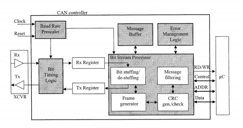
Furthermore, each block can be validated individually, avoiding the need to troubleshoot a whole, complex device, as is the case with sound software engineering principles. The transformation from design definition to usable code is made easier by defining the specifications as a set of requirements or pseudo code.
Factor
Impact Factor 7.894
Journal for Research in Applied Science & Engineering Technology (IJRASET)

ISSN: 2321 9653; IC Value: 45.98; SJ Impact Factor: 7.538 Volume 10 Issue IX Sep 2022 Available at www.ijraset.com
The CAN controller core is being built from the group up, the following parts outline the specifications for moving to HDL. However, since the CAN core has already been established, the following specifications describe how it was built.
The first block that a bus message encounters is the bit timing logic (BTL). This block continually monitors the bus line input and handles the related bit timing according to the CAN protocol. When the BTL detects a transition from recessive to dominant, it synchronizes on that edge and reception of a new frame can begin.

The BTL provides programmable time segments to compensate for delays. Bit timing configuration is programmed in two separate registers. The bit timing logic is the first block that a bus message encounters (BTL). This block continuously tracks the bus line input and manages the CAN protocol related bit timing.
When the BTL detects a recessive to dominant transformation, it synchronizes on that edge, allowing new frame reception to begin. However, as stated in Chapter 2, the sampling point is affected by propagation delays and phase changes. To compensate for delays, the BTL offers programmable time segments. Two registers are used to program the bit timing configuration.
The transmit and receive registers serialize messages to be sent and parallelize messages that are received. These registers hold the data stream bits to allow access to the data by the bit stream processor (BSP), which controls the loading and shifting of the registers.
The bit stream processor (BSP) performs several protocol tasks. The BSP translates messages into frames and frames into messages. Messages are stuffed and destuffed within the BSP and undergo CRC checking while in the BSP
While the bus is idle, the bus is in the recessive state. Arbitration is initiated with a change from recessive to dominantvia the start of frame bit. Every successive bit transmitted is compared with the bus level as illustrated in the state diagram in Figure 2. If the transmitted level matches the bus level, then the next bit is transmitted. If the bus level does not match the transmitted level, then the node either becomes a receiver or there is an error. Once a node has completed the arbitration process, the rest of the message is transmitted.
The indexing of the data frame is known depending on the CAN format (standard or extended). When a result, as the received message is acknowledged, the indexing may be used to evaluate the frames that refer to it. The arbitration sector, for example, is made up of the first 12 bits in the data
Impact Factor
Impact Factor 7.894
International Journal for Research in Applied Science & Engineering Technology (IJRASET)

ISSN: 2321 9653; IC Value: 45.98; SJ Impact Factor: 7.538
Volume 10 Issue IX Sep 2022 Available at www.ijraset.com
The SOF is the first bit in that field, followed by 11 bits that define the identifier field. With this format defined, the frame generator simplyreads the message stream and begins indexing the message once the SOF is received. As a result, the first bit is saved in a register labelled SOF, while the remaining 11 bits are saved in a register labelled identifier. Thesameholds truefor the remainingmessage and the correspondingfieldsrelatedtothe data frame.
Bit stuffing is the process of inserting non information bits into data to break up bit patterns to affect the synchronous transmission of information. The controlled deletion of the stuffed bits from a stuffed signal in order to recover the original signal that existed prior to stuffing of the data bits is the process involved in de stuffing. The bit stuffing method is used on the SOF, arbitration field, control field, and CRC sequence frame segments. After detecting five consecutive bits of the same value, the transmitter inserts a complementary bit into the message stream. When getting a message, the stuff bits are extracted and the message is broken down into frames.
Define:
T (X) = (k + n) bit frame
M(X) = k bit message
P(X) = (n + 1) bit divisor
F (X) = n bit FCS
T is the concatenation of M and F, where M is shifted tothe left n bits.
T should be exactly divisible by P. Divide X"M(X) by P(X).
Thereisaquotientandaremainder,theremainderbecomestheFCS
Now divide T by P.
However, sincearithmetic operationsaremodulo 2:
R(X) + R(X) = 0
Therefore T(X)/P(X)= Q(X)
There is no remainder and therefore, T is exactly divisible by P.
Upon the completed transmission of the data field, the cyclic redundancy check (CRC) field enables a receiving node to verify the integrity of the received data. CRC is one of the most common and powerful, error detecting codes. In general, CRC is described as follows. Given a k bit block of bits or messages, a transmitter generates an n bit sequence, known as a frame check sequence (FCS). The resulting frame, which is k + ii bits long, is exactly divisible by predetermined number. After receiving the message, a receiver will then divide the received frame by the predetermined number. If there is no remainder after the division, the receiver will conclude that there was no error. The CRC procedure can be implemented in three different ways: modulo 2 arithmetic, polynomials and random logic. When the CRC procedure is represented as a polynomial, all values of the polynomial are expressed as a dummy variable X with binary coefficients. The coefficients correspond to the bits in the binary message. Thus, for a binary message M=110011, the polynomial form is M(X)= X5+X4+Xl+1. The coefficients of the frame polynomial are formed by every bit value from the SOF to the final data bit, extended by 15 least significant coefficients of value 0. This polynomial is then divided by the generator polynomial, X15 ± X14 ± X10+X8 + X7 + X4 ± X3+ 1
This division can be implemented by means of a random logic circuit, more specifically a 15 bit linear feedback shift register. The CRC delimiter bit is followed by the 2 bit acknowledgement field, which consists of an acknowledgement slot and an acknowledgement delimiter. A transmitting node transmits the two acknowledgement bits high and then awaits reception acknowledgement of the transmitted frame by at least one receiver. When a validation is received, the receiving node acknowledges the transmitter by writing zeros in the acknowledgement slot. The completion of the data frame is signalled by a sequence of seven recessive bits, referred to as the end of frame flag (EOF), combined with the recessive acknowledgement delimiter bit. Together, these eight bits indicate an error free transmitted frame.
SJ Impact Factor 7.538 | ISRA Journal Impact Factor 7.894 |
Engineering Technology (IJRASET
ISSN: 2321 9653; IC Value: 45.98; SJ Impact Factor: 7.538 Volume 10 Issue IX Sep 2022 Available at www.ijraset.com

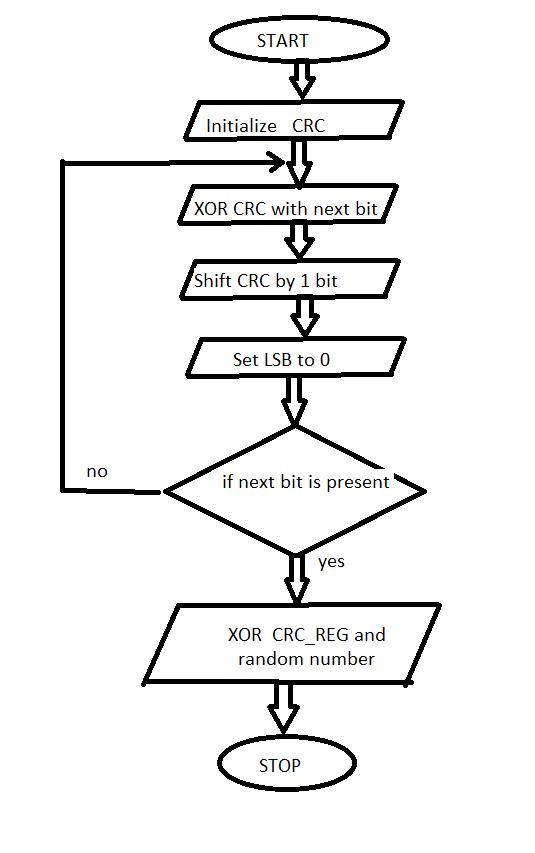
As defined in, one part of the BSP generates the CRC code to be transmitted within the data frame and checks the CRC code of incoming messages. Figure 3.5 shows how the CRC sequence can be generated using an HDL using an analogous 15 bit shift register CRC REG (14:0) implementation with pseudo code. Following the completion of a data frame, the resulting CRC sequence is stored in the 15 bit register.
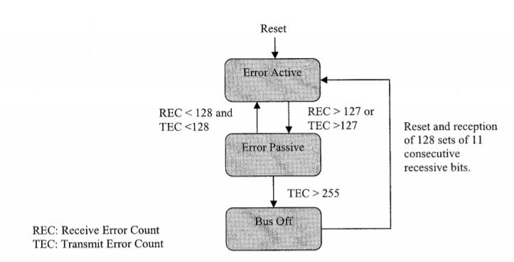
As it processes the data stream, the BSP is constantly checking for errors. When the BSP senses a breach in any of the mechanisms, it generates an error and informs the error management logic (EML). In response, depending on the situation, the EML increments either a receive error counter (REC) or a transmit error counter (TEC). Whether or not the error occurred during transmission or reception is unknown. The values of the error counter determine whether the controller is in an error active, error passive, or bus off mode, according to the CAN protocol. The various error states allow error confinement, which ensures that a defective node does not block communications on its own. Error confinement, which ensures that a defective node does not block communications along the bus, is possible thanks to the various error states. When errors are observed, a node in the error active state participates in regular communications while also sending an active error flag. An error passive node with a high error count can still participate in communications, but it can only send passive error flags ifthere are any more errors found. The bus communications are not disrupted bythe passive error flag. Finally, a nodein the bus off stateis not permitted to communicate with other nodes on the bus. ACAN node's error statediagram is shown in Figure4.
Factor
Technology
ISSN: 2321 9653; IC Value: 45.98; SJ Impact Factor: 7.538 Volume 10 Issue IX Sep 2022 Available at www.ijraset.com

After a reset, a CAN node is immediately placed in an error active state. Once either one of the error counters exceeds 127, the node then enters the error passive state.
The custom RAM used in this project is a two port 64x8 RAM which has separate read and write clocks along with read and write signals. Since it is a 64x8 RAM this can store 64 words of size 8 bits. Vector array named memory is used to store all these words. The RAM has 8 bit data input and 8 bit data output signals. Since it has 64 different locations 6 bit address lines are required to access the data from the RAM or to write data to the RAM. On the positive edges of the respective clocks (read clock, write clock) the corresponding operations will be performed if the read signal / write signal is enabled. This custom RAM is integrated to FIFO as well as BSP modules.
The CAN controller core was simulated after the synthesis was completed. A testbench was used to model the configuration of the CAN controller. A testbench is a hierarchical top level model that instantiates a desired model, the system under test, and other variables. The model is driven by a collection of test vectors, and the model's responses are generated. The testbench created a CAN controller core and then constructed a CAN message with one data byte for the purposes of this thesis. The messages were then sent out, and the CAN controller received them, which were then placed in the receive queue. FIFO has been debated. The following preliminary findings were obtained using the ISE design suite environment. A CAN node transmits a message in its configuration with the receiver line connected to the transmitter line to enable self reception of the transmitted message. This simulation will measure the function of the CAN node.

A register is implemented implicitly with a register interference. During logic synthesis, the compiler automatically inserts an instance of register and connects it as specified in the procedural program code. We can also implement register explicitly with module instantiations.
Fig.
International Journal for Research in Applied Science & Engineering Technology (IJRASET)

ISSN: 2321 9653; IC Value: 45.98; SJ Impact Factor: 7.538 Volume 10 Issue IX Sep 2022 Available at www.ijraset.com
The waveform of CAN register module is shown in Fig.5 and the corresponding console was obtained. From the simulation result, we can see the output of Register module for given 8 bit inputs. Hence, the obtained output matches expected output. Register data are used as variables in procedural blocks. They store logic values only. Here it is disguised as the given input data and the obtained output data are same. For every 5 seconds the input signals data has been changed and the corresponding output data signals have been achieved accordingly. The register elements cannot be connected to the output port of a module instantiation.

Inverse Bit Order has been obtained for the given input data bit order. Thus, the bit inversion using Inverse Bit Order module inverses the input bit order which leads to inverted bit order for the given input data.

The waveforms of the Inverse Bit order module shown in Fig. 6 and the corresponding console has been verified. From the simulation result, we can see that the output of the Inverse Bit order module for the given input 01010000 and obtained corresponding output is 00001010.
It refers to a FIFO design where data values are returned to a FIFO buffer from one clock domain and the data values are read from the same FIFO buffer from another clock domain, where the two clock domains are asynchronous to each other.
The waveforms of the Simulation of FIFO module shown in Fig. 7 and the corresponding console has been verified. From the simulation result, we can see that the output of the Simulation of FIFO module for the given input 00001010 and obtained corresponding output is 00001010.
Rights are Reserved | SJ Impact Factor 7.538 | ISRA Journal Impact Factor 7.894 |
ISSN: 2321 9653; IC Value: 45.98; SJ Impact Factor: 7.538

Volume 10 Issue IX Sep 2022 Available at www.ijraset.com
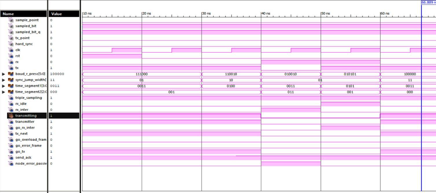
The waveforms of the Simulation of Bit Timing Logic (BTL) module shown in Fig. 8 and the corresponding console has been verified. From the simulation result, we can see that the output of the Simulation of Bit Timing Logic (BTL) module for the given input rst = 1 rx = 0 tx = 1 baud_r_presc = 56 sync_jump_width = 1 time_segment1 = 3 time_segment2 = 1 triple_sampling = 1 rx_idle = 0 rx_inter = 0 transmitting = 1 transmitter = 1 go_rx_inter = 0 tx_next = 1 go_overload_frame = 0 go_error_frame = 0 go_tx = 1 send_ack = 1 node_error_passive =0 and the obtained corresponding outputs are sample_point=0 sampled_bit=1 sampled_bit_q=1 tx_point=0

The test bench has been designed with data input that presents a stream of data which varies with time pulse. Whenever the CRC has to be reset the initialize signal is made high. The stream of data in test bench is passed by keeping the enabling signal high.
Fig. 9 Simulation of Cyclic Redundancy Check module
International Journal for Research in Applied Science & Engineering Technology (IJRASET)

ISSN: 2321 9653; IC Value: 45.98; SJ Impact Factor: 7.538 Volume 10 Issue IX Sep 2022 Available at www.ijraset.com
The waveforms of the Simulation of Cyclic Redundancy Check module shown in Fig. 9 and the corresponding console has been verified. From the simulation result, we can see that the output of the Simulation of Cyclic Redundancy Check module for the given input stream of data the CRC module has performed the necessary mathematical calculations and generated the corresponding CRC for the message signal.
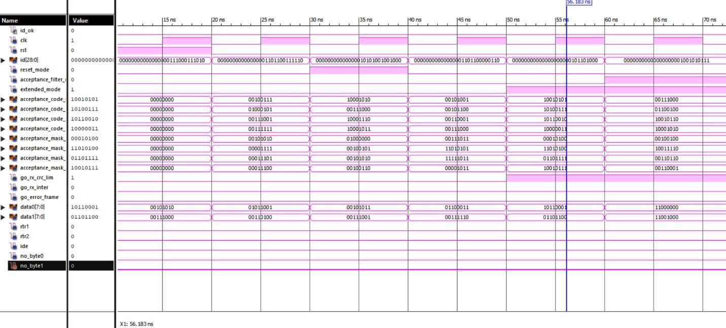
The waveforms of the Simulation of Acceptance Check Filter module shown in Fig. 10 and the corresponding console has been verified. From the simulation result, we can see that the output of the Simulation of of Acceptance Check Filter module for the given input20clk=0 rst =0 id = 6974 reset_mode = 0 acceptance_filter_mode = 0 extended_mode=0 acceptance_code_0=39, acceptance_code_1=69, acceptance_code_2=57, acceptance_code_3=63, acceptance_mask_0=42,acceptance_mask_1=15 acceptance_mask_2 = 29 acceptance_mask_3 = 28 go_rx_crc_lim = 0 go_rx_inter = 0 go_error_frame = 0 data0 = 89 data1 = 52 rtr1 = 0 rtr2 = 0 ide = 0 no_byte0 = 0 no_byte1 = 0 and the obtained corresponding output id_ok=1.
The Addition of custom RAM to the design made the CAN module more invincible, as it can be implemented on any FPGA or microcontroller without the need of any explicit RAM. The proposed architecture of the design has been studied from various sources. This design implementation works in count of three steps. In the first step the can module has been disintegrated into functioning sub blocks: Bit Stream Processor, Bit Timing Logic, Cyclic Redundancy Check module, Acceptance Check Filter, First in First Out module, Inverse Bit Order and registers. In the second step a custom RAM of size 64x8 is designed with separate signals for read and write using Verilog HDL which is integrated in FIFO and BSP. In the final step of the design all the Verilog implementations of the sub blocks are first synthesized and simulated and then integrated together in the top level module that forms the CAN module.
All Rights are Reserved | SJ Impact Factor 7.538 | ISRA Journal Impact Factor 7.894 |
International Journal for Research in Applied Science & Engineering Technology (IJRASET)

ISSN: 2321 9653; IC Value: 45.98; SJ Impact Factor: 7.538 Volume 10 Issue IX Sep 2022 Available at www.ijraset.com
The significant reduction in the proposed architecture offers a great advantage in the reduction of area and therefore the complexity. Thus, the proposed design of CAN is more handy in virtual simulations. The potential applications of this CAN equipped with custom RAM fall mainly in areas where there is strict requirement on accuracy and low space consumption. The Verilog implementation of CAN module helps in implementing CAN through FPGAs thereby reducing the cost of an extra IC and the chance of failure of the system due to the IC. The methodologies and results presented in this thesis suggest a promising approach for the design of CAN and integrating custom RAM to it.
Future scope of the work includes improving the transmission speed and security of CAN design by using enhanced methods and interfacing with indigenous processors like Shakti, which rely on RISC V architecture can be a competitive model for other processors.
[1] “Controller Area Networks: Evolution and Applications”, IEEE, Vol 10, No. 1109,16 84.2006
[2] N. Murphy, "Introduction to Controller Area Network (CAN)," Netrino, Vol. 36 July 2008 [Accessed February 2015].
[3] Rugved D. Katyarmal, Prof. P. Daigavane, “Design of Controller Area Network for Sensor Network Application using Verilog HDL” IJERT Volume 03, Issue 04 (April 2014)
[4] E. e. a. Pathyil, "ECSE Design Final Report: Controller Area Network (CAN) Version 1.6.," Rensselaer Polytechnic Institute, Troy, NY, 2009.
[5] Prof. Stephen St. Michael “Introduction to Controller Area Network (CAN)” https://www.allaboutcircuits.com/technical articles/introduction to can controller area network/, February, 2019.
[6] T. Riesgo, Y. Torroja, J. Uceda “CAN in Automation e. V. CiA 301 V4.2.0 CAN open application layer and communication profile, Feb. 2011
[7] Feng Luo, Jie Chen “Research on CAN controller conformance test system” ICCSIT. 2nd IEEE International Conference on Computer Science and Information Technology, 2009
[8] Marino, Anthony Richard, "HDL implementation of a controller area network node", Theses and Dissertations 1341,2003.
[9] Wang Xing, Huiyan Chen, Huarong Ding “The application of controller area network on vehicle” IVEC International Vehicle Electronics Conference.2013
[10] M. Krug, A. Schendl, "New Demands for In Vehicle Networks," Euromicro: Proc. of the Euromicro Conference, Vol. 23, pp. 601 605, 2011.
[11] M. Guardigli, "Hacking Your Car," Only Dead Fish Go¬ With the Flow, 4 October 2010. http://marco.guardigli.it/2010/10/hacking your car.html, January 2012.
[12] D. A. Sawant, "Passenger Cars: Application Examples," 2011. http://www.can cia.org/index.php?id=187, February 2012.
[13] Janek Tabun, Sven Nomm, " National Instruments CAN Device Simulator,"Available: sine.ni.com/nips/cds/view/p/lang/en/nid/201709. May 2019.
[14] M. Passemard, "Microcontrollers for Controller Area Network (CAN)," Atmel, 2011.
[15] Harshal Hemane1, Debarati Sen2, Atal Tiwari3 “Interfacing CAN Protocol with PIC Microcontroller” IRJET, Volume 05, Issue: Sep 2018.
[16] M. D. Baldania; A. B. Patki; A. M. Sapkal “Verilog HDL based implementation of a fuzzy logic controller for embedded systems” IEEE volume10, No: 1109, Issue: Jan 2018.
Mohd. Ziauddin Jahnagir has a research experience of more than 4 years. He is working as an Assistant professor in ECE Department at Chaitanya Bharathi Institute of Technology. His educational qualification is Doctor of Philosophy (ECE). He received best paper award at IEEE INDICON 2015, International Conference held at Jamia Milia University, New Delhi, December 2015.

Mr. Vijay Bhaskar Nittala is a young researcher pursued Bachelor of Engineering in Electronics and Communication at Chaitanya Bharathi Institute of Technology, Hyderabad. He has been trained in System Verilog, Computer Architecture and Engineering. His research areas of interest are VLSI and Computer Engineering.

Factor
Factor 7.894
