https://doi.org/10.22214/ijraset.2023.49029

ISSN: 2321-9653; IC Value: 45.98; SJ Impact Factor: 7.538

Volume 11 Issue II Feb 2023- Available at www.ijraset.com

https://doi.org/10.22214/ijraset.2023.49029

ISSN: 2321-9653; IC Value: 45.98; SJ Impact Factor: 7.538

Volume 11 Issue II Feb 2023- Available at www.ijraset.com
Abstract: The paper gives a detailed study of how to design a microstrip patch antenna array for UWB applications by using the FR-4 substrate material. The rectangular antenna array is designed with the planar ground. The designed antenna is a rectangular shape, compact and planar for the UWB applications. The size of the antenna is 20.50×15.22 mm (width and length), which resonated at a return loss – 14 dB, -31.23 dB and -33.36 dB and the input impedance is 50 ohms. We used the box dimensions are 40 mm × 40 mm for single, 80 mm × 70 mm for 1×2 array and 100 mm × 40 mm for 1×4 array antenna. For the simulation work SONNET software is used, SONNET software is a planar 3D electromagnetic simulator and all the simulated results are shown by the graph.
Keywords: Rectangular, Microstrip patch antenna, Array, Return loss.
An antenna is a device that converts an RF signal travelling on a conductor through an electromagnetic guided wave in spare space and vice versa. Every antenna is adjusted towards a specific frequency band and rejects signals outside of that range. As a result, antennas may be thought of as band pass filters and transducers. Moreover, in sophisticated wireless systems, an antenna is typically necessary to maximise radiation energy in some directions while suppressing it in others [1].
In 2002, FCC approved the UWB technology in the frequency range of 3.1-10.6 GHz with the maximum radiated power 41.3 dBm/MHz data rate between 110-200 Mbps within 10 m distance (FCC,2002) [2]. Ultra-wide band (UWB) antennas have various uses in the communication systems along with spread- spectrum and broadband in the many radar systems [3]. Microstrip patch antenna has many advantages like lightweight, small size, low fabrication price, planar configuration and low profile. Patch antennas of this calibre are considered fashionable these days. Despite these benefits, the microstrip patch antenna has some drawbacks, including low efficiency, high Q, low power handling capability, very narrow bandwidth, and spurious feed radiation. Various methods can be used to improve the performance of an antenna.
The WLAN applications requires in many wireless devices. Microstrip antennas are capable of operation at different frequencies simultaneously. It’s good numerous features also increase the use of the antenna which has investigated of such antenna by many researchers in many ways. But the major disadvantage of the antenna is the narrow band. There are several techniques have been used to overcome this problem like increasing the substrate thickness and modification of the shape and dimension of the patch [4].
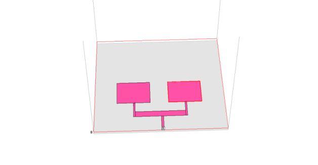
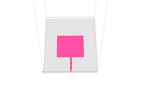
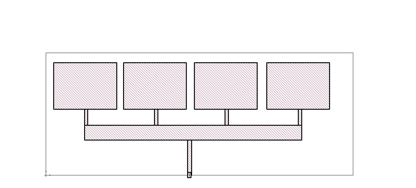
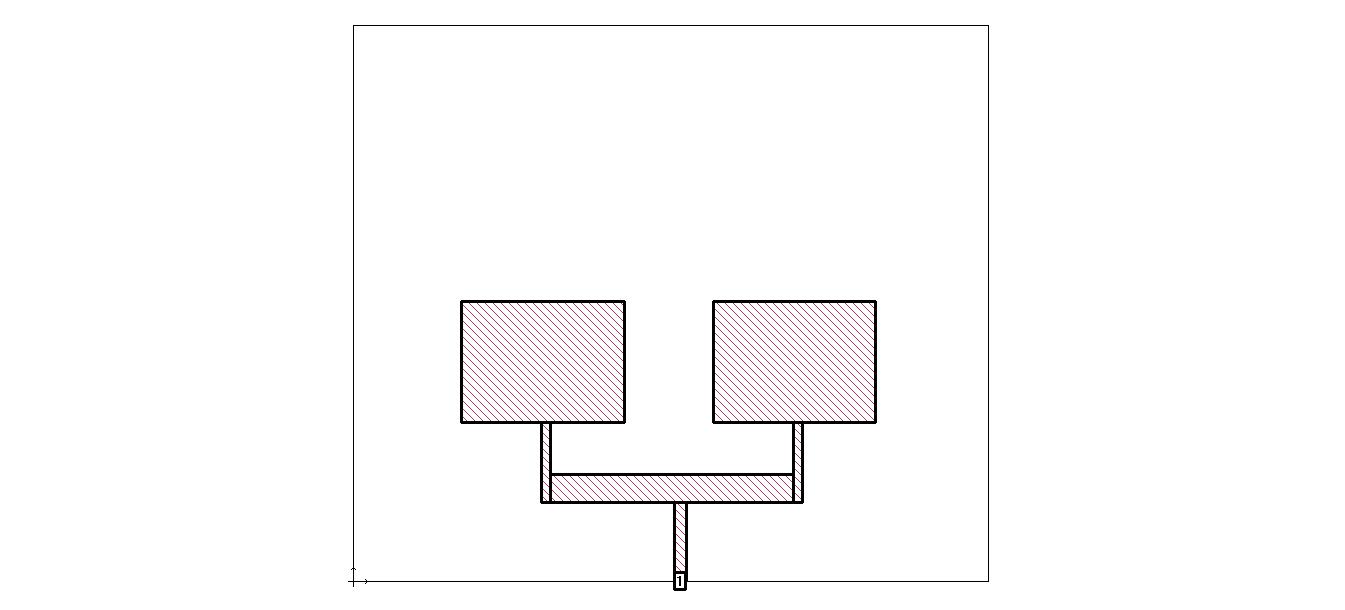
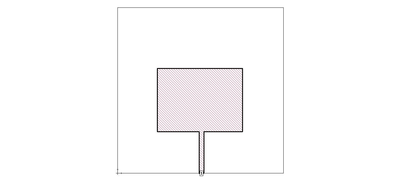
In the procedure of designing, we used the box dimensions are 40 mm × 40 mm for single, 80 mm × 70 mm for 1×2 array and 100 mm × 40 mm for 1×4 array antenna. Dielectric thickness is 1.6 mm and dielectric constant 4.9 for FR-4 and dielectric loss tangent is 0.025 is same for all the antennas. The work begins with a low return loss of below -15 db are gained for the single rectangular antenna, but the gain was high. So we used some array geometry to increase the return loss. Firstly, we used the single rectangular geometry to see the return loss of the decided dimension then make the 1×2 and 1×4 array geometry with some changes to achieve the desired return loss. The frequency of the antenna is between 4-4.5 GHz.
The patch antenna initiates its characteristic on a dielectric substrate which has some electrical and magnetic properties, so choosing an appropriate substrate is equally important. The practical dimensions are calculated of the rectangular patch antenna are calculated by using the following sets of formulas [1]:
2) Length

ISSN: 2321-9653; IC Value: 45.98; SJ Impact Factor: 7.538
Volume 11 Issue II Feb 2023- Available at www.ijraset.com
3) Patch Length Extension
4) Effective Length
5) Effective Dielectric Constant
In the above equations, is the resonant frequency, is the dielectric constant of the substrate material, h is the height and w is the width.
A microstrip patch antenna consists of a radiating patch on one side of a dielectric substrate and has a ground plane on the other side as shown in Fig. 1. The patch is basically made with some conducting materials like gold or copper and in different shapes [5]. The feed lines and the radiating patches are basically photo etched on dielectric substrate. The substrate thickness or height increases, the quality factor Q of the patch decreases [6].
Design parameter of the proposed antenna array is shown in table1.


ISSN: 2321-9653; IC Value: 45.98; SJ Impact Factor: 7.538
Volume 11 Issue II Feb 2023- Available at www.ijraset.com
(c)
(c)


ISSN: 2321-9653; IC Value: 45.98; SJ Impact Factor: 7.538
Volume 11 Issue II Feb 2023- Available at www.ijraset.com
The designed antenna is to be used for the UWB applications specifically for the wireless local area network (WLAN). The dielectric material used is FR-4 which has a dielectric constant 4.9. The thickness of the dielectric material is selected for the better efficiency, better radiation and return loss. The proposed antenna array is simulated by using SONNET software. The important parameter is return loss which is helpful to calculate the bandwidth of the antenna structure is its S11 parameter in decibel verses frequency. The comparison return loss of the proposed antenna array is shown in Fig.4, which resonated at a return loss of -14 dB,31.23 dB and -33.36 dB and the input impedance is 50 ohms.


ISSN: 2321-9653; IC Value: 45.98; SJ Impact Factor: 7.538
Volume 11 Issue II Feb 2023- Available at www.ijraset.com
A proposed microstrip patch antenna array at 4 - 4.5 GHz frequency with 50 ohms input impedance. The proposed antennas performance was improved in terms of thickness of the feed line and thickness of the substrate material. We used the same dimensions for all the antennas with different box sizes. The return loss increased as we increased the number of antennas in the array. The single rectangular microstrip patch antenna at 4.36 GHz with 50 ohms input impedance has a smooth return loss of12.14 dB but as we increased the number of antennas in the series, we get the high return loss but at different frequency. Designs of two element patch antennas and four elements patch antennas are presented in this paper. The overall simulation results proved that the proposed microstrip patch antenna array in terms of gain, size and bandwidth.


[1] S Constantine A. Balanis “Antenna Theory: Analysis and Design,” 3rd Edition, 2005 John Wiley and Sons, Inc. Hoboken, New Jersey.
[2] S Constantine A. Balanis ,Antenna Theory: Analysis and Design, 3rd Edition, John Wiley and Sons, Inc. Hoboken, New Jersey, 2005.
[3] NEWS Federal Communication Commission High Frequency releases, 2002.
[4] Seok H. Choi, Jong K. Park, Sun K. Kim, and Jae Y. Park, A new Ultra-Wideband Antenna for UWB Applications, MICROWAVE AND OPTICAL TECHNOLOGY LETTERS / Vol. 40, No. 5, March 5 2004.

ISSN: 2321-9653; IC Value: 45.98; SJ Impact Factor: 7.538
Volume 11 Issue II Feb 2023- Available at www.ijraset.com
[5] Jain, K., and Sharma, S., Dual Band Rectangular Microstrip Antenna for Wireless Communication Systems, International Journal of Innovations in Engineering and Technology (IJIET), 2 (4), 235-246, 2013
[6] K.C. Gupta, R. Garg, I. Bahl and P Bhartia, Microstrip Lines and Slotlines, ARTECH HOUSE, INC, 1996.
[7] Sharma and G. Singh, Design of single Pin Shorted Three Dielectric Layered Substrates Rectangular Patch Microstrip Antenna for Communication Systems, Progress In Electromagnetics Research Letters, 2008, Vol. 2, pp 157-165.
[8] J. Young and L. Peters, A brief history of GPR fundamentals and applications, Proc. 6th International Conference Ground Penetrating Radar, Sendai, Japan, 1996, pp. 5-14.
[9] Sonnet Software, version 12.56, www.sonnetsoftware.com, 2009.
