1 minute read
Chapter 5 Jumper and Connector Locations


Jumper and Connector Locations
Top View
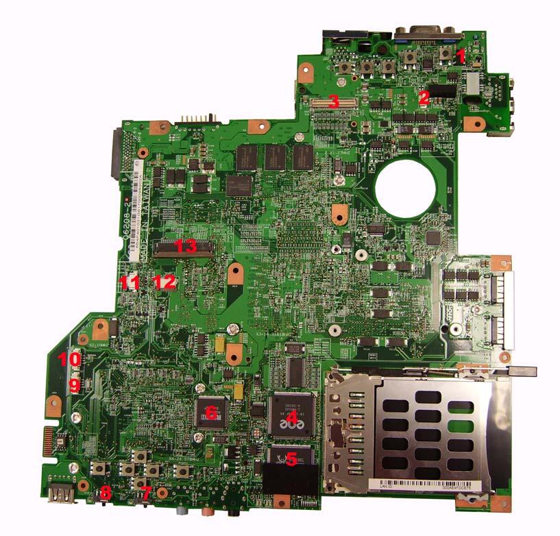
1 CVR1 LID switch 8 BTBTN1 Bluetooth launch switch 2 MIC1 Microphone cable connector 9 SPK1 Speaker set cable 3 LCD1 LCD cable connector 10 BT1 Bluetooth module cable connector 4 U38 Cardbus controller (ENE CB-1410)11 LEDB1 LED FFC connector 5 U43 LAN controller (Realtek RTL8100CL) 12 TAPD1 Touchpad cable connector 6 N/A Card reader controller (Ricoh R5C832) 13 KB1 Keyboard cable connector 7 WLBTN1 Wireless launch switch
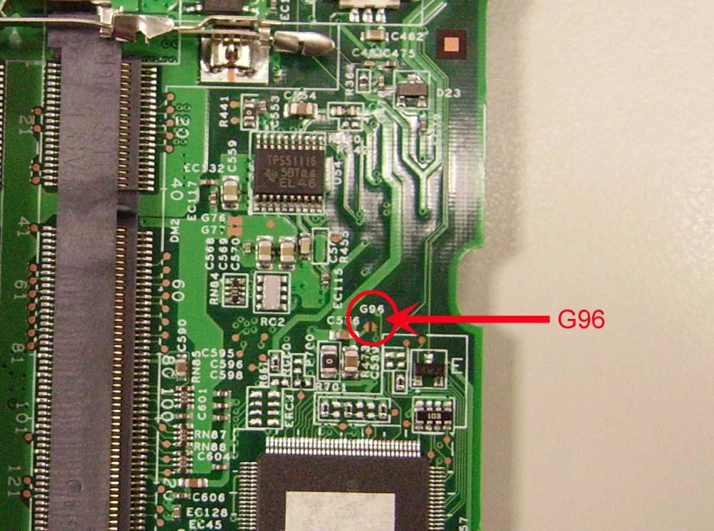
NOTE: This is engineering sample. The image above may not be exactly the same as the real main board you get.
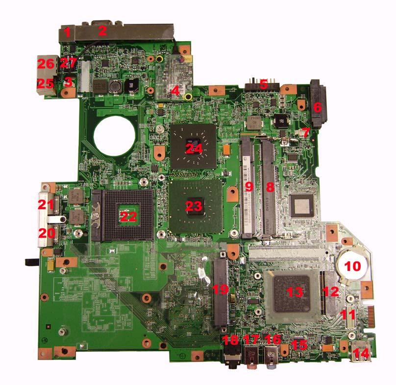
1 DCIN1 DC-in jack 14 USB3 USB port 2 CRT1 External display port 15 U67 Audio codec (Reltek ALC833) 3 N/A Modem cable connector 16 LIN1 Line-in jack 4 MDC1 Modem board connector 17 MIC2 Microphone jack 5 BAT1 Battery connector 18 LOUT1 Headphone/speaker/line-out jack 6 CDROM1 ODD module connector 19 HDD1 HDD module connector 7 FAN1 System fan connector 2021 USB1 USB ports 8 DM2 DIMM 2 socket 22 U58 CPU socket 9 DM1 DIMM 1 socket 23 U56 North Bridge 10 RTC1 RTC battery 24 U53 VGA controller 11 CN2 Card reader board connector 25 TRING1 Modem jack 12 MINIC1 Wireless LAN card slot 26 RJ1 LAN jack 13 U62 South bridge (Intel ICH7M)
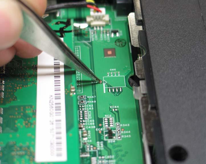
1. Remove the DIMM cover and the lower DDR2 memory module, then find out the G96 position on the main board. Please just the lower DDR2 memory module, you will need the upper DDR2 memory module to boot up the system. (You should tear off the mylar to see G96).
2. Use a tweezers or a screwdriver to short the G96 pad and remain the short status.
3. Power on the system until POST is completed. Then you can release the tweezers or screwdriver. The
BIOS password should be cleared after these steps.