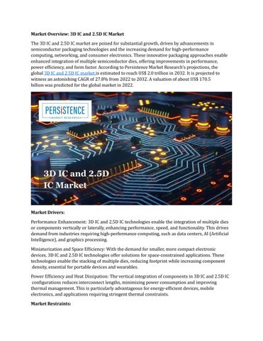
Market Overview: 3D IC and 2.5D IC Market
The 3D IC and 2.5D IC market are poised for substantial growth, driven by advancements in semiconductor packaging technologies and the increasing demand for high-performance computing, networking, and consumer electronics. These innovative packaging approaches enable enhanced integration of multiple semiconductor dies, offering improvements in performance, power efficiency, and form factor. According to Persistence Market Research's projections, the global 3D IC and 2.5D IC market is estimated to reach US$ 2.0 trillion in 2032. It is projected to witness an astonishing CAGR of 27.8% from 2022 to 2032. A valuation of about US$ 170.5 billion was predicted for the global market in 2022.
Market Drivers:
Performance Enhancement: 3D IC and 2.5D IC technologies enable the integration of multiple dies or components vertically or laterally, enhancing performance, speed, and functionality. This drives demand from industries requiring high-performance computing, such as data centers, AI (Artificial Intelligence), and graphics processing.
Miniaturization and Space Efficiency: With the demand for smaller, more compact electronic devices, 3D IC and 2.5D IC technologies offer solutions for space-constrained applications. These technologies enable the stacking of multiple dies, reducing footprint while increasing component density, essential for portable devices and wearables.
Power Efficiency and Heat Dissipation: The vertical integration of components in 3D IC and 2.5D IC configurations reduces interconnect lengths, minimizing power consumption and improving thermal management. This is particularly advantageous for energy-efficient devices, mobile electronics, and applications requiring stringent thermal constraints.
Market Restraints:
Complexity and Cost: Implementing 3D IC and 2.5D IC technologies involves sophisticated manufacturing processes, including wafer bonding, through-silicon via (TSV) fabrication, and interposer integration, leading to higher manufacturing costs. The complexity of design and testing further adds to the overall cost, limiting adoption, especially among smaller players and costsensitive applications.
Design Challenges: Designing for 3D IC and 2.5D IC architectures requires specialized expertise and tools, posing challenges for designers in optimizing performance, signal integrity, and thermal management. The lack of standardized design methodologies and ecosystem support complicates adoption and hampers time-to-market for new products.
Interconnect and Packaging Reliability: The reliability of interconnects and packaging remains a concern in 3D IC and 2.5D IC implementations, with issues such as signal degradation, thermal stress, and reliability failures impacting device performance and longevity. Addressing these reliability challenges requires advancements in materials, manufacturing techniques, and testing methodologies.
Market Opportunities:
Emerging Applications: The proliferation of emerging applications such as 5G telecommunications, autonomous vehicles, augmented reality (AR), and IoT devices presents significant growth opportunities for 3D IC and 2.5D IC technologies. These applications demand high-speed data processing, low latency, and compact form factors, driving adoption of advanced packaging solutions.
Heterogeneous Integration: 3D IC and 2.5D IC technologies facilitate heterogeneous integration, enabling the co-packaging of different semiconductor technologies such as logic, memory, sensors, and RF (Radio Frequency) components. This integration enables new functionalities, improves system-level performance, and accelerates innovation in diverse application domains.
Supply Chain Collaboration: Collaboration across the semiconductor supply chain, including foundries, OSATs (Outsourced Assembly and Test) providers, EDA (Electronic Design Automation) vendors, and equipment suppliers, is essential for advancing 3D IC and 2.5D IC technologies. Strategic partnerships and ecosystem collaborations can drive standardization, reduce costs, and accelerate time-to-market for advanced packaging solutions.
Read More: https://www.persistencemarketresearch.com/market-research/3d-ic-and-2.5d-icmarket.asp
Market Segmentations:
By Packaging Technology
3D Wafer-level Chip-scale Packaging
3D Through-silicon Via
2.5D
By Application
Logic
Imaging and Optoelectronics
Memory
Micro-electromechanical Systems/Sensors
Light-emitting Diode
Power
Analog & Mixed Signal
Radio Frequency
Photonics
By End User
Consume r Electroni cs
Telecom municatio n
Industry Sector
Automoti ve
Military and Aerospac e
Smart Technolo gies
Medical Devices
By Region
North America
Latin America
Europe
Asia Pacific
Middle East and Africa
Regional Market Dynamics: North America: North America leads the 3D IC and 2.5D IC markets, driven by technological innovation, strong R&D investments, and the presence of major semiconductor players. The region is hub
Asia-Pacific: Asia-Pacific emerges as a key market for 3D IC and 2.5D IC technologies, fueled by the presence of semiconductor manufacturing hubs, strong demand for consumer electronics, and rapid digitalization across sectors. Countries such as China, Taiwan, South Korea, and Japan are at the forefront of technology adoption, driving market expansion in the region.
Key Players:
The 3D IC and 2.5D IC markets feature a diverse ecosystem of players, including semiconductor manufacturers, packaging providers, design houses, and equipment suppliers. Some prominent players in the market include:
Taiwan Semiconductor Manufacturing Company
Intel Corporation
United Microelectronics Corporation
Samsung Electronics Co., Ltd.
ASE Group
Amkor Technology
ST Microelectronics NV
Broadcom Ltd.
Jiangsu Changjiang Electronics Technology Co., Ltd
Toshiba Corporation
Market Trends & Latest Developments:
Advanced Packaging Technologies: Continuous innovation in advanced packaging technologies such as fan-out wafer-level packaging (FOWLP), system-in-package (SiP), and chip-on-wafer-onsubstrate (CoWoS) drives efficiency, performance, and reliability in 3D IC and 2.5D IC implementations.
AI-driven Design Automation: AI (Artificial Intelligence) and machine learning technologies are increasingly integrated into EDA (Electronic Design Automation) tools, enabling faster design iterations, optimization, and predictive analysis for complex 3D IC and 2.5D IC designs.
Heterogeneous Integration Platforms: Heterogeneous integration platforms and design methodologies facilitate seamless integration of diverse semiconductor technologies, enabling customized solutions for specific application requirements in areas such as automotive electronics, IoT, and edge computing.
Future Trends and Outlook:
Multi-Chip Integration: Future advancements in 3D IC and 2.5D IC technologies will focus on multichip integration, enabling the co-packaging of heterogeneous components such as logic, memory, sensors, and photonics to meet the demands of emerging applications.
AI-driven Optimization: AI-driven optimization techniques will play a significant role in improving design productivity, performance, and reliability in 3D IC and 2.5D IC implementations, enabling faster time-to-market and enhanced product differentiation.
Sustainable Packaging Solutions: Sustainable packaging solutions, including recyclable materials, eco-friendly processes, and energy-efficient designs, will gain prominence in the 3D IC and 2.5D IC markets, aligning with global sustainability initiatives and consumer preferences.
The 3D IC and 2.5D IC markets are poised for dynamic growth, driven by advancements in semiconductor technology, increasing demand for high-performance computing, and the proliferation of IoT and AI applications. Market players must navigate challenges related to cost, design complexity, and reliability while capitalizing on emerging opportunities in diverse industry verticals and geographic regions to maintain competitive advantage in the rapidly evolving semiconductor ecosystem.
Follow Us: LinkedIn | Medium | Twitter
About Persistence Market Research:
Business intelligence is the foundation of every business model employed by Persistence Market Research. Multi-dimensional sources are being put to work, which include big data, customer experience analytics, and real-time data collection. Thus, working on “micros” by Persistence Market Research helps companies overcome their “macro” business challenges.
Persistence Market Research is always way ahead of its time. In other words, it tables market solutions by stepping into the companies’/clients’ shoes much before they themselves have a sneak pick into the market. The pro-active approach followed by experts at Persistence Market Research helps companies/clients lay their hands on techno-commercial insights beforehand, so that the subsequent course of action could be simplified on their part.
Contact Us:
Persistence Market Research G04 Golden Mile House, Clayponds Lane, Brentford, London, TW8 0GU UK
Email: sales@persistencemarketresearch.c om
Web: https://www.persistencemarketr esearch.com