INTERNATIONAL


From everyday applications such as mobile phones and banking to complex underwater defense missions, the need for synchronized precise timing and frequency solutions is critical to safeguard and process data as intended. Many of these applications rely on Global Navigation Satellite Systems (GNSS) to provide that precise time and frequency, but GNSS is susceptible to jamming and spoofing attacks. To provide multiple industries - including telecommunications, data centers, metrology, aviation and defense - with a longterm and precise timing and frequency solution, Microchip Technology announces the 5071B cesium atomic clock that can perform autonomous time keeping for months in the event of GNSS denials. Microchip’s 5071B is the next-generation commercial cesium clock to the existing 5071A, which has been the primary contributor to international time for more than three decades. The 5071B is available in a three-unit height (3U) 19-inch rackmount enclosure, providing a compact product to work in environments where it can be easily transported and secured versus a larger alternative designed specifically for laboratory environments.
The 5071B has upgraded electronic components to address possible obsolescence or non-RoHS circuitry. The product provides 100 ns holdover for more than two months, maintaining system synchronization when GNSS signals like GPS are denied. For example, this capability would enable a 5G network to remain fully operational for months without GNSS.
As a cesium beam tube product with no deterministic long-term frequency drift, the 5071B provides absolute frequency accuracy of 5E-13 or 500 quadrillionths over all specified environmental conditions for the life of the product.
For military applications requiring rapid deployments for system radars, 5E-13 stability eliminates the need for the acquisition of external synchronization sources prior to radiating. In satellite communications, this enables the user to broadcast and transmit over very small frequency bands without drifting out of band for the entire duration of the product. When deployed, a product like the 5071B could maintain and better synchronize the critical communication between an aircraft and control tower.
Air traffic control in the United States utilizes the Automatic Dependent Surveillance -Broadcast (ADS-B) and Wide Area Multilateration (WAM) to precisely locate the position of aircraft across the nation’s airspace. The stability of the 5071B enables more accurate locations and continued operation during GNSS outages.
The 5071B is now fully compliant with the Restriction of Hazardous Substances Directive (RoHS), making this product available in regions where regulatory policies are in place.
Microchip provides the broadest portfolio of clock and timing systems in the industry. Its state-of-the-art solutions are based on the company’s long heritage in the field of synchronization and timing and vertical integration of its core timing technologies.
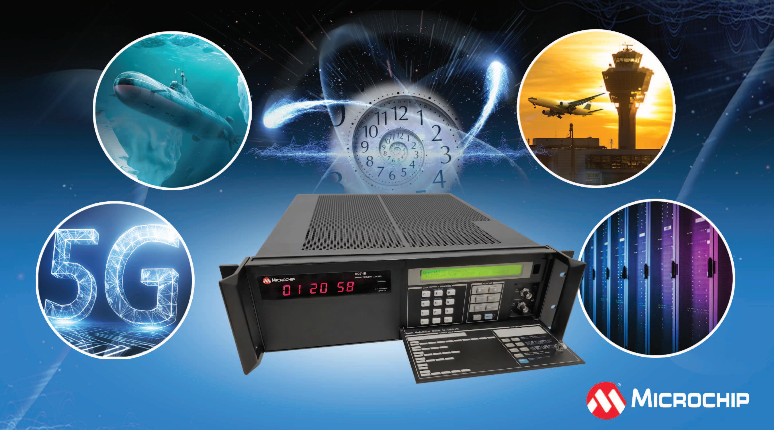


The 5071B cesium atomic clock is supported by Clockstudio™ Software Tool to control and monitor data.
Microchip Technology


www.microchip.com

3 | New Cesium Atomic Clock Provides Autonomous Precise Time of 100 ns Holdover for Months
6 | Mouser Electronics Shares the Revolutionary Power of Digital Therapeutics in Latest Empowering Innovation Together Series
7 | Infineon further extends its edge AI capabilities and choice-of-platforms for Machine Learning-based models for Bluetooth customers by partnering with Edge Impulse
8 | Bringing the in-vehicle sound experience to the next level: Asahi Kasei Microdevices launches sales of AK7709VQ multicore DSP for automotive applications
45 | Posifa Technologies Introduces New Hydrogen Sensors for BMS Thermal Runaway Detection
45 | Renesas Automotive MCU and SoC Cybersecurity Management Certified to ISO/SAE 21434:2021

47 | Renesas Develops Complete Power Management Solution for AMD Space-Grade Versal Adaptive SoC

48 | Vicor introduces new e-book into its power module resource library to support aerospace, defence and satellite applications
49 | TE Connectivity drives adoption of Single Pair Ethernet standard with SPE Industrial Partner Network

50 | TASKING presents TriCore Qualified C Library for functional safety
50 | New eBook from Mouser Electronics and Renesas Electronics Explores Industrial IoT Design Opportunities with TinyML
10 | Improving Power Supply Design Using Semi-Automation
20 | How smart peripherals help automate low-level tasks in microcontroller systems
24 | How Autonomous Vehicles Will Improve Sustainability and Productivity in Agriculture

51 | Mouser Electronics Unlocks Transformative Industrial Solutions Through Extensive Resource Hub
52 | SiC 650V Schottky barrier diodes with forward voltage of 1.2V released by Toshiba
52 | Microchip Introduces Its First Automotive-Qualified 10BASE-T1S Ethernet Devices
53 | Optical Spectrum Analyzer MS9740B Enhances
High-Power Laser Diode Measurement Function
54 | Renesas Introduces R-Car S4 Starter Kit That Enables Rapid Software Development for Automotive Gateway Systems
54 | Farnell adds the new BeagleV®-Ahead single board computer to its portfolio
55 | DigiKey Adds 175,000+ New SKUs Year-to-Date in 2023
29 | New memory technology for innovative IoT applications

34 | The future of agriculture will be more sustainable, connected than ever
36 | From the blue light of Thyratron to Wide Band Gap semiconductors
40 | Walking the razor thin line: Balancing power and performance in embedded systems
Management
Managing Director - I onela G anea
Editorial Director - Gabriel N eagu
Accounting - I oana P araschiv

Advertisement - Irina G anea
Web design - Eugen Vărzaru
Contributing editors

Cornel Pazara
PhD. Paul S vasta
PhD. N orocel C odreanu
PhD. Marian Blejan
PhD. B ogdan G rămescu
VAT: RO3998003 | Tel.: +40 (0) 31 8059955 | Tel.: +40 (0) 744 488818 office@electronica-azi.ro | https://international.electronica-azi.ro

56 | Nexperia unveils industry’s first coin cell battery life and power booster
56 | PLS Extends Support for Infineon’s TRAVEO™ T2G MCUs
57 | Anritsu 5G Base Station Simulator Integrated in SPEAG DASY8-3D V1.4 5G
58 | Sensors with convincing cost effectiveness on conveyor lines and in the packaging industry
“Electronica Azi” is a registered trademark at OSIM - Romania, Registered position: 124259
ISSN: 1582-3490



Mouser Electronics Inc., the industry’s leading New Product Introduction (NPI) distributor with the widest selection of semiconductors and electronic components™, premieres its latest instalment of the Empowering Innovation Together (EIT) series unveiling the transformative potential of digital therapeutics. Mouser examines the bridge between technology and medical devices to find how these parts and components can work together to provide a more personalised and accessible means of healthcare.
The medical industry is constantly evolving, and technology has become a crucial aspect in changing traditional methods. Digital therapeutics have emerged as an efficient approach that offers the potential to reach more patients, monitor conditions in real time, and reduce the financial barriers to accessing medical care. To support this shift, Mouser and its industry-leading supplier partners have collaborated to share their collective expertise and promote a more comprehensive method of personal health.
The latest series instalment includes a brand-new podcast episode from The Tech Between Us, as well as a second episode from In Between The Tech, featuring esteemed guests from the Digital Medicine Society and Freespira.
Each episode breaks down the meaning of digital therapeutics and the cutting-edge solutions it has the potential to provide.
Through these informative episodes, listeners will gain a comprehensive understanding of the technical hardware and software aspects of engineering design, along with the current industry challenges facing this area.
Mouser’s articles, case study and infographics offer a comprehensive exploration of the present market landscape while also presenting an optimistic outlook on future prospects, such as advancements in wearable technology, FDA approval procedures, and the diverse range of treatments it can facilitate.
The range of content helps provide a solid foundation and raise awareness among designers about how to incorporate modern solutions into digital therapeutic devices.
This EIT instalment is sponsored by Mouser’s valued partners ams Osram, Microchip Technology, Bourns, Murata, NXP Semiconductors, Molex, and Renesas.
Established in 2015, Mouser’s Empowering Innovation Together program is one of the industry’s most recognised electronic component programs.
To learn more, visit the web page: https://eu.mouser.com/empoweringinnovation/ and follow Mouser on Facebook, LinkedIn, Twitter and YouTube
For more Mouser news, visit the web page: https://eu.mouser.com/newsroom/
Mouser Electronics www.mouser.com
Infineon Technologies announced it is teaming with Edge Impulse to extend its Tiny Machine Learning-based AI devel opment tools for the PSoC™ 63 Bluetooth® LE microcontroller (MCU). Developers of AI-enabled IoT applica tions can now also build edge Machine Learning (ML) applications using the Edge Impulse Studio environment for deployment on high-performance, lowpower PSoC 63 Bluetooth LE MCUs. This collaboration allows customers added flexibility and choice-of-platforms to natively develop and configure ML applications for systems based on PSoC 63 Bluetooth LE MCU devices, which provide 150-MHz Arm® CPU performance with lowpower connectivity and a rich suite of peripheral options. For example, the CY8CKIT-062-BLE Pioneer Kit coupled with the E-Ink Display Shield Board (CY8CKIT028-EPD) incorporates an inertial measurement unit, microphone, and temperature sensor. This supports applications that collect real-world sensor data for processing by Tiny Machine Learning-based AI models in systems optimized for low-power, low-cloud-cost edge IoT environments.
Infineon’s PSoC 63 Bluetooth LE MCU devices feature a dual-core Arm® Cortex®M4F and Arm Cortex-M0+ chip architecture, Bluetooth LE 5.2, configurable voltage and frequency settings, built-in hardware-based security, state-of-the-art capacitive interfaces, and more, on a single chip. As the only 150 MHz Bluetooth LE MCU on the market, this variant of the
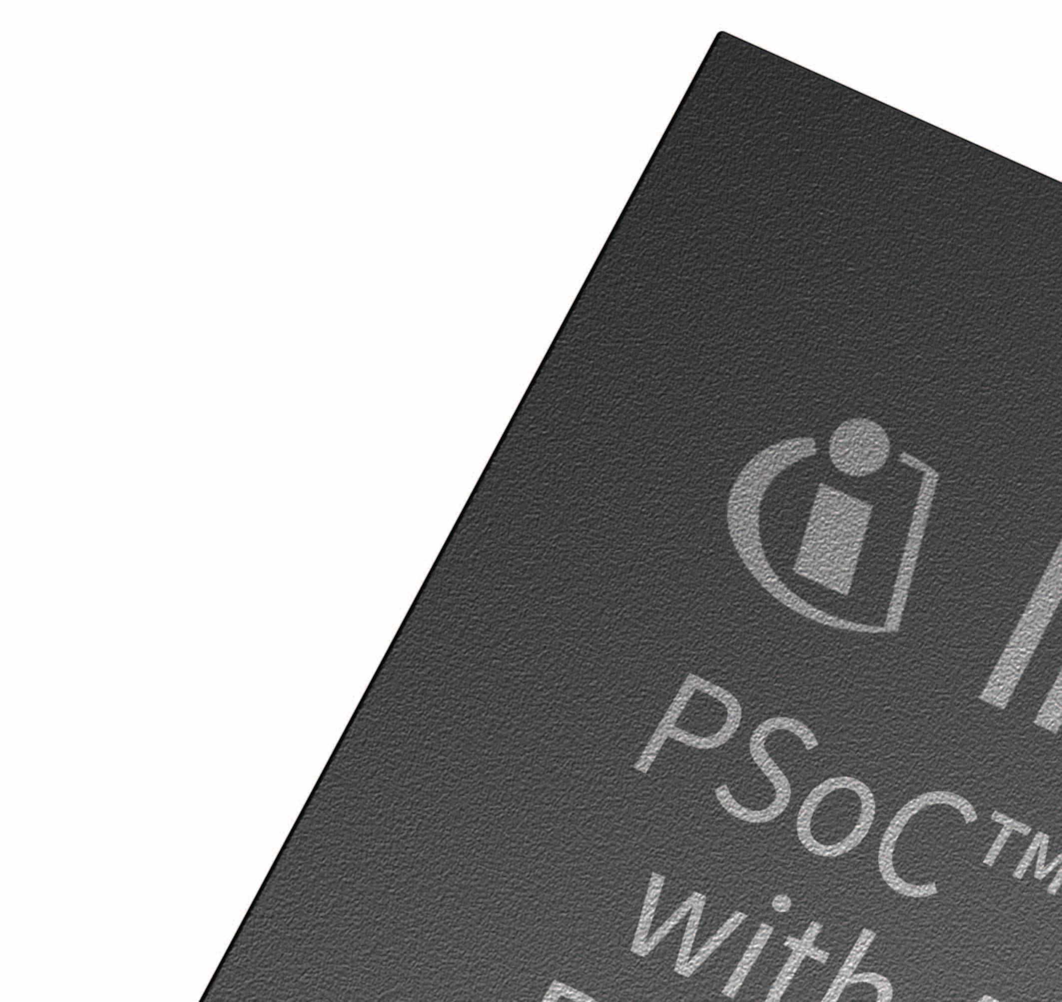

Infineon PSoC device family is a powerful combination of power efficiency, size, and programmability making it perfectly suited for edge IoT applications that benefit from the ability to run advanced ML algorithms. Edge Impulse’s products streamline the entire process of collecting and structuring data sets, designing algorithms with pre-built building blocks, validating the models with real-time data, and deploying the fully optimized production-ready results to edge targets such as the PSoC 63 Bluetooth LE MCU.
“By collaborating with Edge Impulse on the PSoC 63 Bluetooth LE MCU, Infineon customers can bring their solutions faster to market for embedded AI/ML use cases. Infineon is committed to enable our customers to develop their own AI/ML models, or use a model out of suite of predefined models available from Infineon or our valuable partners. Infineon is excited to add Edge Impulse to our growing partner network, and will continue to work with our extensive group of AI/ML partners that complements our offerings,” said Shantanu Bhalerao, Vice President of the Bluetooth Product Line at Infineon. “With its advanced processing capabilities and low power consumption, the PSoC 63 Bluetooth LE MCU is an ideal vehicle for the
next generation of edge devices, from wearables to industrial monitoring,” said Zach Shelby, CEO and co-founder of Edge Impulse. “Matched with the Edge Impulse platform, embedded developers can more quickly develop and deploy powerful solutions for an exciting range of edge ML applications.”
More information about the CY8CKIT062-BLE Pioneer Kit is available here.
Edge Impulse enables all enterprises to build smarter edge products. Their technology empowers developers to bring AI solutions to market faster, and helps enterprise teams rapidly develop industry-specific solutions in weeks instead of years. Edge Impulse provides powerful automation and low-code capabilities to make it easier to build valuable datasets and develop advanced AI with streaming data. With over 75,000 developers, and partnerships with the top silicon vendors, Edge Impulse offers a seamless integration experience to validate and deploy with confidence across the largest hardware ecosystem (www.edgeimpulse.com).


Asahi Kasei Microdevices (AKM) has launched the AK7709VQ, a new multicore digital signal processor (DSP) conceived for next-generation in-vehicle sound design. This powerful DSP enables the real-time large-scale computational processing required to provide an immersive sound experience for passengers.

With the advent of self-driving cars, there will be less need for passengers to focus on the traffic, allowing more time to be spent on work, entertainment, or relaxation. As passengers’ expectations for the automotive environment evolve, the ability to create a customized, quiet setting with an accompanying premium listening experience will become a key differentiator for the in-cabin user experience.
As a total solution provider for the in-vehicle sound environment, AKM has provided premium sound technology used in cars around the world for more than 20 years. Bringing its expertise in the field of active
premium sound to the next level, the company’s launch of the new AK7709VQ DSP further boosts the potential for a natural and immersive in-vehicle sound experience.
With a processing capability of 7,000 MIPS (Millions of Instructions per Second) and 2.75 MB of integrated memory, the AK7709VQ performs real-time high-resolution audio processing for multi-channel speaker arrays, enabling a quiet cabin with immersive, incredibly detailed music playback.
Additionally, the two integrated HiFi 4 DSP cores support various third-party software. The AK7709Q’s unique feature set, which features high sample rate multi-microphone voice processing, also allows for hands-free and in-car communication. The built-in audio hub function, which includes 20 channels of asynchronous hardware sample rate conversion (ASRC), supports
flexible digital input/output to and from many digital sources and endpoints.
In addition, AKM has applied its acclaimed audio PCB (Printed Circuit Board) design expertise to develop a sound design demo board combining the new DSP with the AK4499EXEQ, AKM’s flagship digital audio converter (DAC). This system demonstrates immersive in-vehicle sound and can be experienced by customers in demo cars at the company’s Garage Labs in Tokyo, Shanghai, and Shenzhen. Additional Garage Labs will make this experience available in North America and Europe in the fourth quarter of 2023.
More information on the product: https://www.akm.com/us/en/aboutus/news/2023/20230720-ak7709
Asahi Kasei Microdevices (AKM) www.akm.com/eu/en
Designing the correct power source is essential and complex, since there is no one typical application. While total automation of power supply design is yet to be achieved, a comprehensive range of semi-automated tools are available today. This article details the use of semi-automated design tools through five critical steps of the power supply design process. These tools can be valuable to both the novice and expert power supply design engineer.
Author: Frederik Dostal Senior Staff Field Applications Engineer, Power Management Analog Devices
Creating the Power Supply Architecture

Creating a suitable power supply architecture is a decisive step in power supply design. This step becomes more complex by increasing the number of needed voltage rails.
At this point, the decision is made as to whether and how many intermediate circuit voltages need to be created.
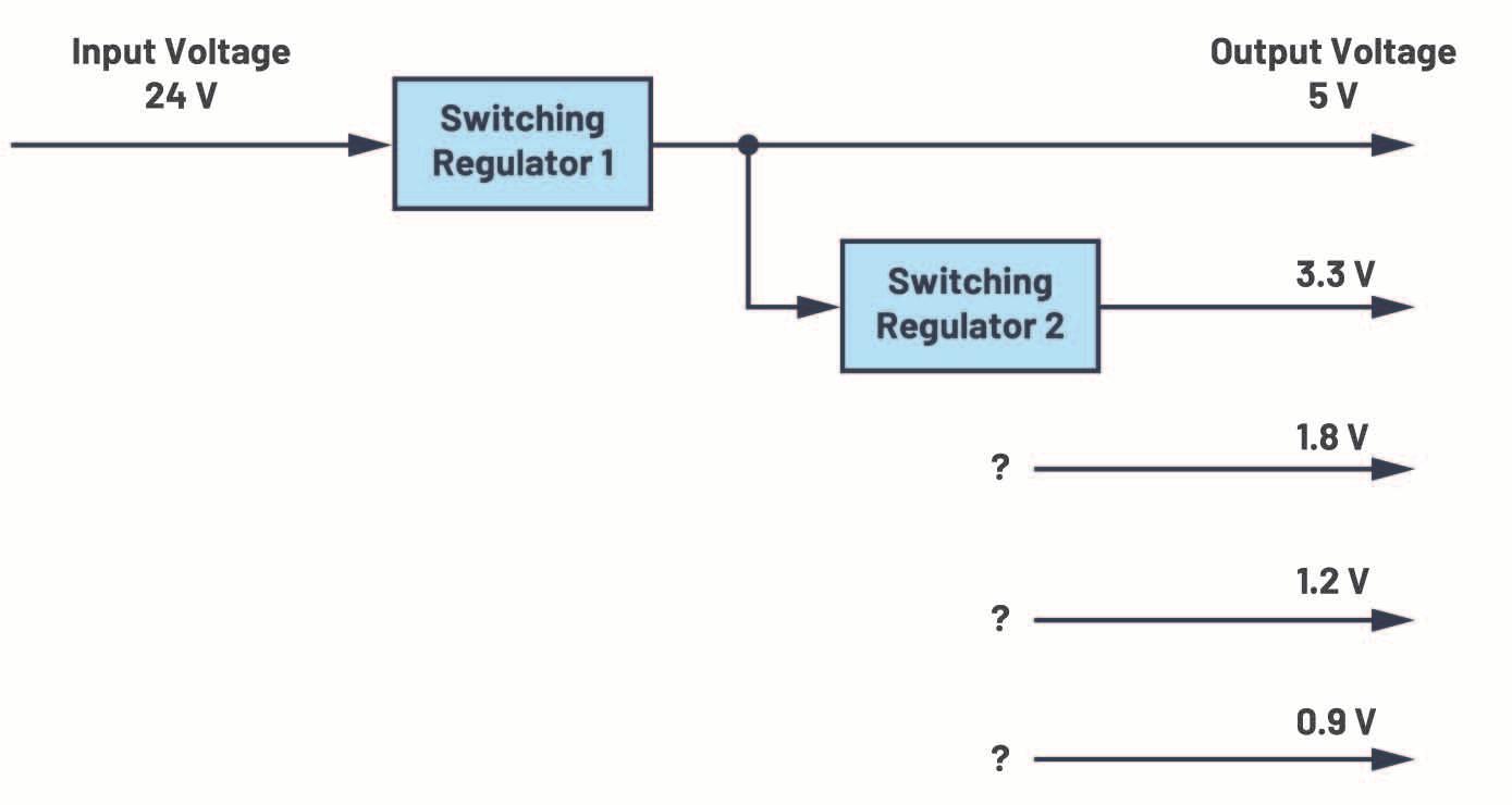
Figure 1 shows a typical block diagram of a power supply. The 24V supply voltage of an industrial application is shown on the left. This voltage must be converted now into 5V, 3.3V, 1.8V, 1.2V, and 0.9V with corresponding currents. What is the best method for generating the individual voltages? Selecting a classic step-down switching (buck) converter makes the most sense for converting from 24V to 5V.
However, how do you generate the other voltages? Does it make sense to generate the 3.3 V from the 5 V already created, or should we convert to 3.3 V directly from 24 V? Answering these questions requires further analysis. Since an important property of a power supply is the conversion efficiency, keeping the efficiency as high as possible is important when selecting the architecture.


If intermediate voltages, such as 5V in the example shown in Figure 1, are used to generate additional voltages, the energy used for the 3.3V must already pass through two conversion stages. Each conversion stage has only limited efficiency. If, for example, a conversion efficiency of 90% is assumed for each conversion stage, the energy for 3.3V, which has already passed through two conversion stages, only has an efficiency of 81%
For higher currents, however, this lower efficiency might have a greater effect on the overall system efficiency and consequently represent a big disadvantage. From the considerations just mentioned, however, you cannot draw the general conclusion that it is always better to convert directly from a higher supply voltage to the lower output voltage in one step. Voltage converters that can handle a higher input voltage are usually more expen-
It is available free of charge from Analog Devices and is part of the LTpowerCAD® development environment, which can be installed locally on your computer. LTpowerPlanner is a tool that makes evaluating different architectures quick and easy.

Finalizing the specification is extremely important in power supply design. All additional development steps depend on the specification. Frequently, the precise requirements of the power supply are unknown until the rest of the electronic system has been completely designed. This usually results in increasing time constraints on power supply design development. It also often happens that the specification is changed in a later development stage. For example, if in its final programming, an FPGA requires additional power, the voltage for a DSP must be reduced to save energy, or the originally intended switching frequency of 1 MHz must be avoided because it is coupled into the signal path. Such changes can have very serious effects on the architecture and, in particular, on the circuit design of the power supply.
(0.9 × 0.9 = 0.81). Can this rather low efficiency be tolerated in a system or not? This depends on the current required from this 3.3V rail. If current of only a few mA is needed, the low efficiency might not be a problem at all.
sive and have a reduced efficiency when there is a greater difference between the input voltage and the output voltage. In power supply design, the solution to finding the best architecture is to use an architecture tool such as LTpowerPlanner®.
A specification is usually adopted at an early stage. This specification should be designed to be as flexible as possible so that it is relatively easy to implement any changes. In this effort, selecting versatile integrated circuits is helpful. Working with development tools is particularly valuable. This allows the power supply to be recalculated within a short time. In this way, specification changes can be implemented more easily and, above all, more quickly.
The specification includes the available energy, the input voltage, the maximum input current, and the voltages and currents to be generated. Other considerations include size, financial budget, thermal dissipation, EMC requirements (including both conducted and radiated behaviors), expected load transients, changes in the supply voltage, and safety.

LTpowerPlanner provides all the necessary functions for creating a power supply system architecture. It is very simple to operate, allowing for rapid concept development. An input energy source is defined and then individual loads, or electrical consumers, are added.
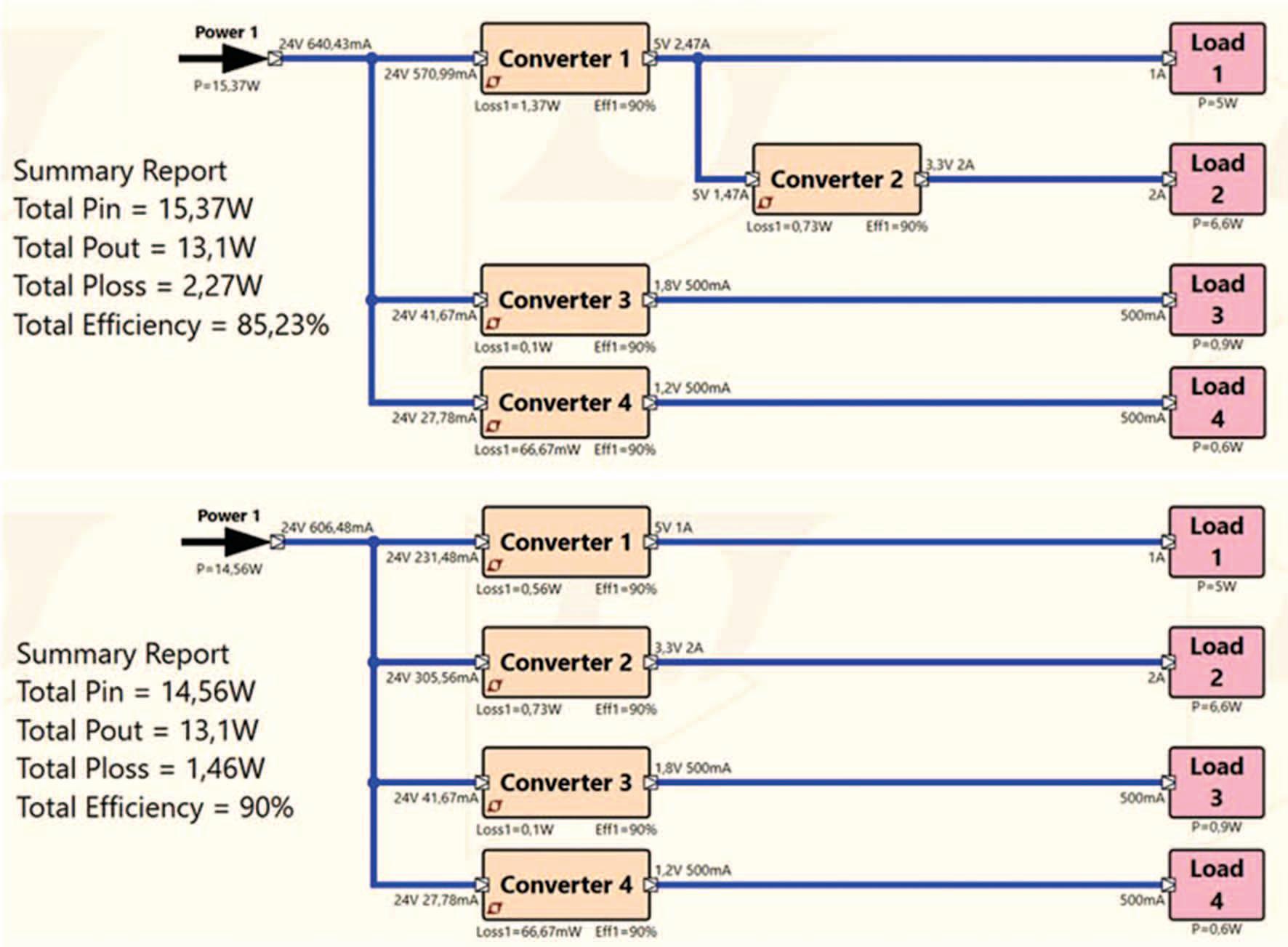
This is followed by adding individual dcto-dc converter blocks. These could be switching regulators or low dropout (LDO) linear regulators. All components can be assigned their own name. An expected conversion efficiency is stored for efficiency calculations.
Using LTpowerPlanner has two great benefits. First, a simple architecture calculation can identify the configuration of
the individual conversion stages most beneficial for overall efficiency. Figure 2 shows two different architectures for the same voltage rails. The architecture at the bottom has an overall efficiency that is somewhat higher than that of the architecture at the top. This property is not evident without a detailed calculation. When using LTpowerPlanner, this difference is immediately revealed.
The second benefit of LTpowerPlanner is that it provides well-organized documentation. The graphical user interface provides a neat sketch of the architecture, a visual aid that can be invaluable in discussions with coworkers and in documenting the development effort.
Documentation can be stored either as a paper hard copy or a digital file.


When designing power supplies today, an integrated circuit is used rather than a discrete circuit with many separate components. There are a multitude of different switching regulator ICs and linear regulators available in the market. All of them are optimized for one specific property. Interestingly, all integrated circuits are different and can be interchanged only in the rarest of cases. Selecting the integrated circuit thus becomes a very important step. Once an integrated circuit has been selected, the properties of that circuit are fixed for the rest of the design process. Later, if it turns out that a different IC is better suited, the effort to incorporate a new IC begins again. This development effort can be very time consuming but can be easily mitigated with the use of design tools.
Based on these specifications, LTpowerCAD generates a list of recommended solutions. Additional criteria can be entered to further narrow down the search. For example, in the Features category you can select from features such as an enable pin or galvanic isolation to find an appropriate dc-to-dc converter.

Step 3 is the circuit design. The external, passive components need to be selected for the chosen switching regulator IC. The circuit is optimized in this step. Usually, this requires studying a data sheet thoroughly and performing all the required calculations. This step in power supply design can be drastically simplified by the comprehensive design tool, LTpowerCAD, and the results can be optimized further.
The transfer function of the control loop is also calculated. This makes it easy to implement the best control bandwidth and stability.
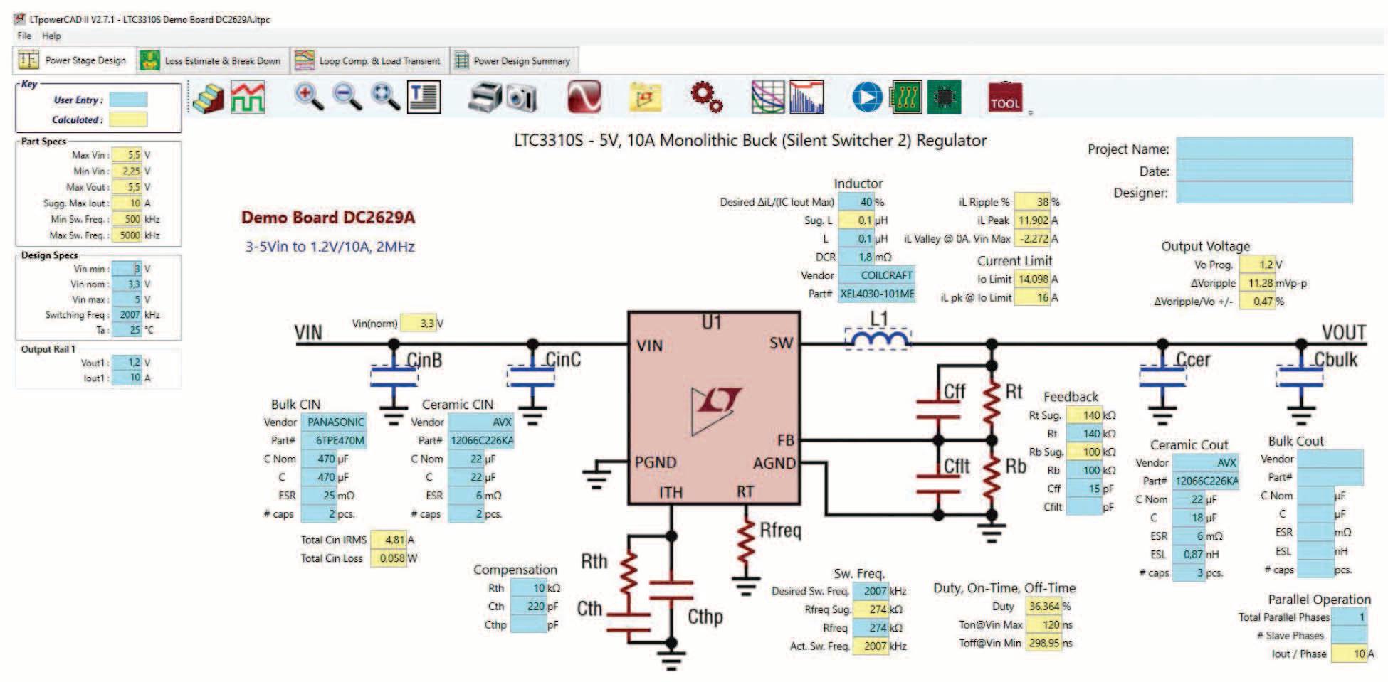
After opening a switching regulator IC in LTpowerCAD, the main screen displays the typical circuit with all the necessary external components. Figure 4 shows this screen for the LTC3310S as an example. This is a step-down switching regulator with an output current of up to 10A and a switching frequency of up to 5 MHz. The yellow fields on the screen show the calculated or specified values. The user can configure settings using the blue fields.
LTpowerCAD reliably simulates the behaviors of a real circuit as calculations are based on detailed models of external components, not just ideal values. LTpowerCAD includes a large database of integrated circuit models from several manufacturers.
Using a tool is critical for effectively selecting the integrated circuit. The parametric search on analog.com is suitable for this. Searching for components within LTpowerCAD can be even more productive. Figure 3 shows the search window. To use the search tool, only a few specifications need to be entered. For example, you may enter the input voltage, output voltage, and required load current.
LTpowerCAD was developed by Analog Devices to greatly simplify circuit design. It is not a simulation tool, but rather a calculation tool.
It recommends, in a very short time, the optimized external components based on the specification entered. The conversion efficiency can be optimized.


For instance, the equivalent series resistance (ESR) of a capacitor and the core losses of a coil are taken into consideration. To select external components, click on a blue external component as shown in Figure 4. A new window will open, showing a long list of possible components.
As an example, Figure 5 shows a list of recommended output capacitors.
This example shows a selection of 88 different capacitors from various manufacturers. You can also exit the list of recommended components and select the Show All option to choose from a variety of more than 4660 capacitors. This list is continuously expanded and
updated. While LTpowerCAD is an offline tool and does not require internet access, regular software updates (using the update function) will ensure that the integrated switching regulator ICs and the database of external components remain up to date.
Checking the Conversion Efficiency

Once the optimal external components have been selected, the conversion efficiency of the switching regulator is checked using the Loss Estimate & Break Down button. A precise diagram of the efficiency and losses is then displayed.


In addition, the junction temperature reached in the IC can be calculated based on the thermal resistance of the housing. Figure 6 shows the page of calculations for the conversion efficiency and thermal behavior. Once you are satisfied with the circuit response, you can move to the next set of calculations. If the efficiency is not satisfactory, the switching frequency of the switching regulator can be changed (see left side of Figure 6), or the selection of the external coil can be changed. The efficiency is then recalculated until a satisfactory result is achieved.
After selecting the external components and calculating the efficiency, the control loop is optimized. The loop must be set so that the circuit is reliably stable, not prone to oscillations or even instability while providing a high bandwidth - that is, the ability to respond to changes of the input voltage and, in particular, to load transients.

Figure 7 shows the LTpowerCAD screen when setting the control loop.
The stability calculations performed in LTpowerCAD are a highlight of its architecture. The calculations are performed in the frequency domain and are very fast, much faster than simulations in the time domain. As a result, parameters can be changed on a trial basis and an updated Bode plot is provided in a few seconds. For a simulation in the time domain, this would take many minutes or even hours.
Depending on the specification, additional filters may be necessary at the input or output of the switching regulator. This is where less experienced power supply developers, in particular, face large challenges. The following questions arise: How must the filter components be selected to ensure a certain voltage ripple at the output? Is an input filter necessary and, if so, how must this filter be designed to
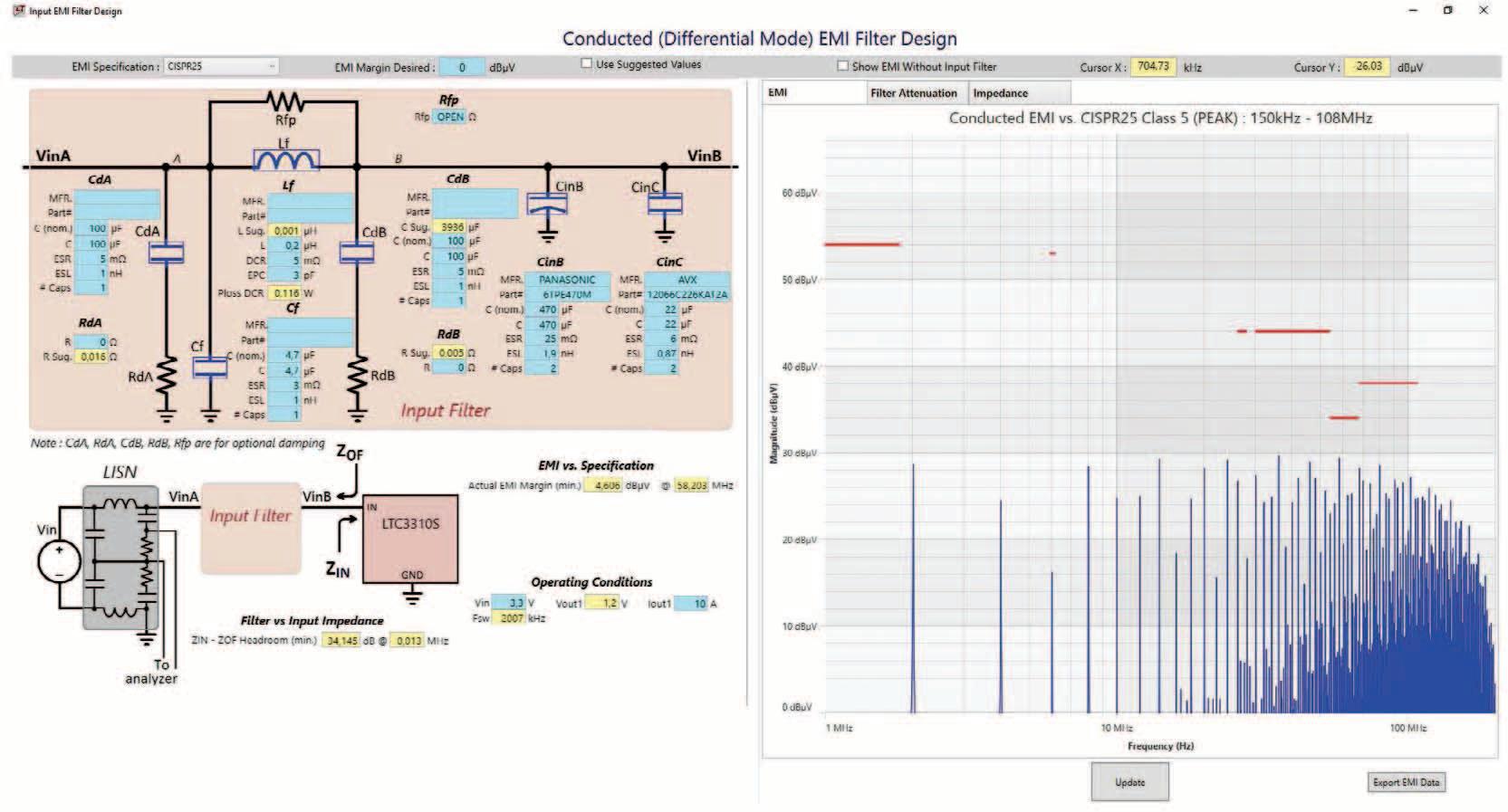
This graph plots the conducted interference with or without an input filter and within appropriate limits from various EMC specifications such as CISPR 25, CISPR 22, or MIL-STD-461G.
The filter characteristic in the frequency domain and the filter impedance can also be displayed graphically beside the illustration of the input conducted EMC response. This is important to ensure that a filter does not have total harmonic distortion that is too high, and that the filter impedance matches the impedance of the switching regulator. Problems with the impedance match can lead to instabilities between the filter and the voltage converter.
Such detailed considerations can be accounted for in LTpowerCAD and do not require in-depth knowledge. With the Use Suggested Values button, the filter design is automated. Of course, LTpowerCAD also supports the use of a filter on the output of the switching regulator.
The stability considerations in LTpowerCAD can be found in the Loop Comp. & Load Transient tab. In addition to a Bode plot and curves on the response of the output voltage following load transients, there are many setting options.
The Use Suggested Compensation button is the most important. In this case, the optimized compensation is used, and the user need not dive deeply into control engineering to adjust any parameters.

keep conducted emissions below certain EMC limits? In this respect, interaction between the filter and the switching regulator must not result in instability under any circumstances. Figure 8 shows the Input EMI Filter Design, which is a sub-tool in LTpowerCAD. This can be accessed from the first page where the external, passive components are optimized. Starting the filter designer brings up a filter design using passive ICs and an EMC graph.
This filter is often used for applications where the output voltage is only allowed to have a very low output voltage ripple. To add a filter in the output voltage path, click the LC filter icon on the Loop Comp. & Load Transient page. Once this icon is clicked, a filter appears in a new window, as shown in Figure 9. The parameters of the filter can be easily selected here. The feedback loop can either be connected in front of this additional filter or behind it.
Here, a stable response of the circuit can be ensured in all operating modes despite very good dc precision of the output voltage.
Simulation of the circuit in the time domain
Once you have completely designed a circuit using LTpowerCAD, simulating it is the crowning achievement. Simulations are usually run in the time domain. Individual signals are checked against time. The interaction of different circuits can also be tested on a printed circuit board.
As a result, it is not always clear to the user of a simulation whether the circuit has already achieved the optimal state. A computing tool such as LTpowerCAD is better suited for this purpose.
Simulating the power supply using LTspice LTspice®, from Analog Devices, is a powerful simulation program for electric circuits. It is very widely used by hardware developers globally, due to its ease of use, extended network of user support, optimization options, and high quality, reliable simulation results.

Both are intuitive to operate, even for a beginner. These features also provide a great deal of flexibility for the experienced user. LTspice is designed to be simple and easy to use. The program, available for download at analog.com, includes a very large database containing simulation models of nearly all power ICs from Analog Devices along with external passive components. As mentioned, once installed, LTspice can operate offline. However, regular updates will ensure that the newest models of switching regulators and external components are loaded. To start an initial simulation, choose an LTspice circuit in the product folder of a power product on analog.com (for example, the LT8650S evaluation board). These are usually the suitable circuits of the available evaluation boards. By doubleclicking the related LTspice link in a specific product folder on analog. com, LTspice will launch the complete circuit locally on your PC. It includes all external components and presets necessary to run a simulation. Then, click on the runner icon, pictured in Figure 10, to start simulation.
It is also possible to integrate parasitic effects into the simulation. With this, the result of the simulation becomes very accurate, but the simulation times are longer. Generally, a simulation is suitable for collecting additional information prior to implementing real hardware. It is important to know the potential and the limits of circuit simulation. Finding the optimal circuit might not be possible using simulation only. During simulation, one can modify parameters and restart the simulation. However, if the user is not an expert in designing circuits, it can be difficult to determine the right parameters and then to optimize them.
Additionally, LTspice is free of charge and can easily be installed on a personal computer. LTspice is based on the SPICE program, which originated from the Department of Electrical Engineering and Computer Sciences at the University of California, Berkeley. The acronym SPICE stands for simulation program with integrated circuit emphasis. Many commercial versions of this program are available. Although originally based on Berkeley’s SPICE, LTspice offers considerable improvements in the convergence of circuits and simulation speed. Additional features of LTspice include a circuit diagram editor and waveform viewer.
Following a simulation, all the voltages and currents of a circuit can be accessed using the waveform viewer. Figure 11 shows a typical illustration of the output voltage and the input voltage as the circuit ramps up. A SPICE simulation is primarily suited for getting to know a power supply circuit in detail so that there are no unwanted surprises when building the hardware. A circuit can also be changed and optimized using LTspice. In addition, the interaction of the switching regulator with the other parts of the circuit on the printed circuit board can be simulated. This is particularly helpful in uncovering interdependencies. For example, several switching regulators can be simulated at the same time in one run. This extends the simulation time, but certain interactions can be checked in this case. Finally, LTspice is an extremely powerful and reliable tool used by IC developers today. Many ICs from Analog Devices have been developed with the help of this tool.
While automation tools have a valuable purpose in power supply design, the next step is to perform a basic hardware evaluation. The switching regulator operates with currents switched at a very high rate. Due to the parasitic effects of the circuit - particularly of the printed circuit board layout -
these switched currents cause voltage offset, which generates radiation. Such effects can be simulated using LTspice. To do this, however, you need precise information about the parasitic properties. Most of the time this information is

not available. You would have to make many assumptions, and these reduce the value of the simulation result.


Consequently, a thorough hardware evaluation must be completed.


The PCB layout is known as a component. It is not possible to operate a switching regulator for test purposes using jumper wires, as it is with a breadboard.

Mainly, the parasitic inductance in the paths where the currents are switched leads to a voltage offset that makes operation impossible. Some circuits could also be destroyed due to excessive voltage.
There is support available for creating an optimal printed circuit board layout. The corresponding data sheets for the switching regulator ICs usually provide information about a reference printed circuit board layout. For most applications, this suggested layout can be used.
During the power supply design process, conversion efficiency is considered to determine whether the switching regulator IC operates within the permissible temperature range. However, testing the hardware at its intended temperature limits is important.
The switching regulator IC and even the external components vary their rated values over the permissible temperature range. These temperature effects can easily be taken into consideration during the simulation using LTspice.
However, such a simulation is only as good as the given parameters. If these parameters are available with realistic values, LTspice can perform a Monte Carlo analysis that leads to the desired result. In many cases, evaluating the hardware through physical testing is still more practical.
In late stages of system design, hardware must pass electromagnetic interference and compatibility (EMI and EMC) tests. While these tests must be passed with real hardware, simulation and calculation tools can be extremely useful in gathering insights. Different scenarios can be evaluated prior to hardware testing.
Certainly, there are some parasitics involved that are usually not modeled in simulation, but general performance trends related to these test parameters can be obtained. Additionally, the data obtained from such simulations can provide the insights necessary to apply modifications to the hardware quickly, in case an initial EMC test was not passed.
Since EMC tests are costly and time intensive, utilizing software such as LTspice or LTpowerCAD in early design stages can help achieve more accurate results prior to testing, thus speeding up the overall power supply design process and reducing costs.
The tools available for power supply design have become very sophisticated and powerful enough to meet the demands of complex systems.
LTpowerCAD and LTspice are high performance tools with simple to use interfaces. As a result, these tools can be invaluable to a designer with any level of expertise.
Anyone from the experienced developer to the less experienced can use these programs to develop power supplies on a day-to-day basis.
It is astounding how much simulation capabilities have evolved. Using the proper tools can help you build a reliable, sophisticated power supply more quickly than ever before.

The Free Power Tools from ADI
Follow these links:
• Optimization help LTpowerPlanner
• Calculation tool LTpowerCAD
• Simulation tool LTspice
■ Analog Devices www.analog.com

About the author
Frederik Dostal studied microelectronics at the University of Erlangen in Germany. Starting work in the power management business in 2001, he has been active in various applications positions including four years in Phoenix, Arizona, where he worked on switch-mode power supplies. He joined Analog Devices in 2009 and works as a field applications engineer for power management at Analog Devices in München. He can be reached at frederik.dostal@analog.com.

Engage with like-minded members and ADI technology experts in our online community, EngineerZone®. Expand your network, ask your tough design questions, share your expertise, browse our rich knowledge base, or read about new technologies and the engineers behind them in one of our blogs.
Visit https://ez.analog.com



The Renesas RA family of Arm Cortex based microcontrollers builds on the rich history of the Renesas microcontrollers that came before, such as the popular H8 or M16C families. The RA family uses or enhances many of the peripheral functions that were originally implemented on these devices. These peripherals have been tried and tested over many years and provide proven and predictable operation. Some also provide unique features that can improve an application’s performance or reduce its power consumption. In this article, we’ll look at how some of these peripherals operate and how they can be combined to automate many of the low-level tasks that have to be managed in a typical microcontroller application.
Autor: Graeme Clark Principal Engineer Renesas Electronics
Probably one of the most interesting - but least understood - peripherals inside a typical RA microcontroller is the Data Operations Circuit (DOC). This can provide significant performance advantages in real time applications by allowing simple tasks to be offloaded from the CPU. This improves the response time and potentially reduces power consumption. This is especially true when the DOC is used in conjunction with some of the other more advanced features available on the RA family.
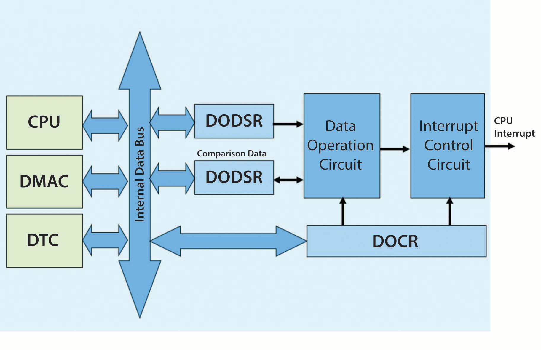
At the heart of the DOC is a simple Arithmetic Logic Unit (ALU). This simple ALU has only three basic functions: it can make a 16-bit data comparison, a 16-bit addition, or a 16-bit subtraction, and then it can generate an interrupt based on a specific output condition. These functions can all be executed without any intervention from the CPU. This is done by automatically transferring the data to be operated on by the DOC, using either a Direct Memory Access Controller (DMAC) or a
Data Transfer controller, which we will explain in a moment. See figure 1 below. When using the 16-bit comparison mode, an initial reference value is loaded into the DOC. The 16-bit data to be compared is then loaded and compared with the reference value in hardware. The DOC can be programmed to generate an interrupt on match true or match false. When using the 16-bit addition mode, an initial 16-bit value is loaded into the DOC. Additional 16-bit values are then loaded (one or more) into the DOC and are added to the original value. When all the required values are loaded, the count is checked for overflow, and an interrupt generated if required.
This simple mechanism allows for a decision to be made if a specific threshold value has been exceeded, ideal for instance for automatic level sensing using the ADC.
However, the true power of the Data Operation Circuit is in the fact that these three simple functions can be used to make decisions as to how the system should operate.
This can be done without any CPU intervention, even when the CPU is asleep. This can provide a much faster response to changing data, rather than waiting for the CPU to be interrupted to then respond to the event.


We can imagine many instances where the DOC could be used. One example is with the analogue to digital converter (ADC) in a level sensing system to detect automatically when the level exceeds a programmed threshold. There are many advantages to using the DOC for functions like these. For instance, the CPU could be dedicated to other high-priority tasks and only be alerted by a DOC interrupt when a particular input condition is reached. The CPU can be placed into sleep to reduce power consumption, and only awakened again by an interrupt on a valid alarm condition detected by the DOC.
When using the 16-bit subtraction mode, an initial 16-bit value is loaded into the DOC. Additional 16-bit values are then loaded (again, can be one or more) into the DOC and are subtracted from the original value.
When all the required values are loaded, the count is checked for underflow, and an interrupt generated if required. This simple mechanism again allows for a decision to be made if a specific threshold value has been breached.
This means that we can make intervene directly in the hardware of the microcontroller, allowing the hardware to decide how to respond to specific input data. When the DOC is combined with peripherals such as the Direct Memory Access Controller (DMAC) or the Data Transfer Controller (DTC), which can automate the passing of data to the DOC, we can see how this can be used to create a system that’s capable of making decisions based on data from almost any source.

The Data Operating Circuit is available on all the members of the RA family. Renesas has continued to enhance the DOC and the latest versions have additional functions, allowing even more complex decisions to be made on data.
Let’s now look at the Data Transfer Controller (DTC) which we mentioned earlier. This is a peripheral that has been designed to provide a simple but extremely flexible mechanism to transfer data between a peripheral and memory or memory and a peripheral. A Data Transfer Controller can be found on all the members of the RA microcontroller family.
The DTC uses a simple programmable controller to make these transfers, keeping its configuration information in a table in SRAM. This is much smaller than using a large, dedicated hardware block for this task, such as is typically used by the Direct Memory Access Controller (DMAC). This programmability provides a much higher level of flexibility compared to using a DMAC. By storing the configuration table describing the transfer in SRAM we can have almost unlimited channels, only restricted by the available amount of SRAM.
On the RA family, an event (or interrupt) triggered by the CPU, a peripheral or an external pin can generate several actions on the device. Figure 2 shows a simplified diagram of the interrupt controller.
It illustrates how an event can trigger several actions. These include a traditional interrupt that changes the program flow of the application; a DMAC transfer; or a DTC transfer. It is also possible to trigger more than one of these from a single event. So, let’s look at the DTC in detail. The use of SRAM to hold the DTC configuration information means that the DTC controller can be used to create not just one or two channels of data transfer, but 10 or 20 or even more if required. The main disadvantage of this mechanism is that for each transfer a few cycles must be taken to read the configuration data held in the SRAM before each transfer takes place. As a result, the DTC transfer is generally slower than a DMA transfer. The DTC can transfer 1 byte or more, between a peripheral and memory or memory and peripheral, up to 256 times. The source and destination address for the transfer each can be the same, or can be incremented or decremented independently, thus creating a buffer structure in memory.
At the end of the transfer, the DTC can generate an interrupt to tell the CPU the data is ready, or it can trigger a second DTC transfer. This can be used to chain several transfers together, which is why this is known as chain mode. Chain mode can be especially useful if the movement of multiple pieces of data between peripherals and memory is required. Chain mode is particularly interesting when used with the DOC we discussed previously, as this means that multiple transfers from various locations in memory and/or a peripheral can be triggered by one interrupt source. For instance, this means that with one interrupt, such as the ADC interrupt, we can cause comparison data to be loaded into the DOC. By chaining a second transfer, we can load the DOC with the data from the ADC to be compared, all completely automatically. This ability for one interrupt to generate a complex sequence of different transfers is extremely powerful, not only when used with the DOC. Some of the different operating modes of the DTC are shown in Figure 3.

The DTC can also be placed into repeat mode, where it will repeat the transfer an additional number of times. For most applications the flexibility of the DTC provides a perfect compromise between speed and flexibility. Users can create automated transfers between any peripheral and memory almost without limit.
This demonstrates how the DTC can be much more flexible than the traditional DMAC. The DMAC is still the faster method if the highest data transfer speeds are required and almost all the RA microcontrollers include a number of DMAC channels. However, for flexibility and easy data management the DTC wins hands down. In addition, users can create multiple channels, only limited by the available SRAM. Let’s now look at how the DTC and DOC can be combined with the ADC to create an intelligent analogue sampling system. This potentially reduces the demand on the CPU and even saves power consumption by putting the CPU to sleep while the ADC, DTC and DOC operate.
The system we want to create is a simple multiple input level detector, which uses the group scan mode of the 12-bit ADC to sample each of 4 input signals in turn. Using the combination of the DTC and the DOC, it detects whether a programmable threshold level is exceeded.
ADC transfer request to DTC.
From the on-chip SRAM, it copies both the 4 ADC results and a corresponding threshold value that each ADC result should be compared against. In this case, we initialise the DOC to compare each value and generate an interrupt if any of the threshold values are exceeded.
DTC transfer 1 Comparison[0] to DOC. Chain Enabled, so do next transfer
DTC transfer 2 AN000 to DOC Chain Enabled, so do next transfer
DTC transfer 3 Comparison[0] to DOC Chain Enabled, so do next transfer
DTC transfer 4 AN001 to DOC Chain Enabled, so do next transfer

DTC transfer 5 Comparison[0] to DOC Chain Enabled, so do next transfer
DTC transfer 6 AN003 to DOC Chain Enabled, so do next transfer
DTC transfer 7 Comparison[0] to DOC Chain Enabled, so do next transfer
DTC transfer 8 AN005 to DOC Chain Disabled, so stop
The system will only generate an interrupt and wake the CPU if this value has been exceeded.


After the initial system setup, the CPU goes to sleep to save power and only awakens if an interrupt from the DOC occurs, indicating that the threshold has been exceeded. A simplified system diagram is shown in Figure 4.
In group scan mode, the ADC continuously samples each input in turn and copies the result into SRAM. When all 4 inputs have been sampled, the ADC generates a DTC request. Using chain mode, this request starts a chain of 8 transfers between memory and the DOC.
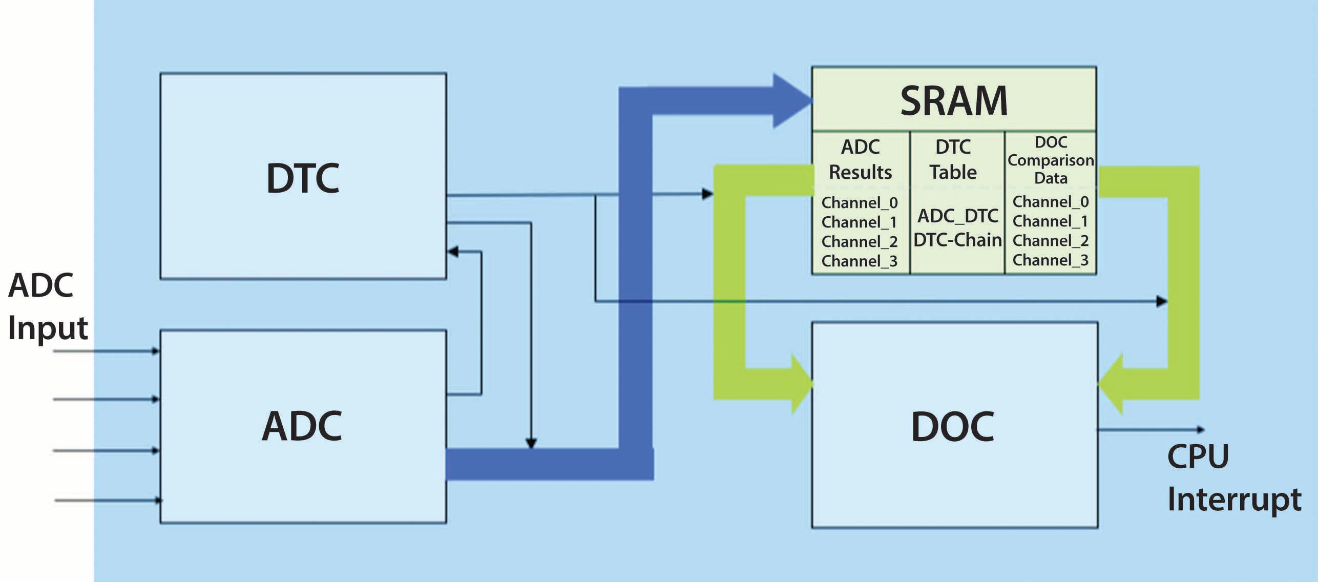
Once the ADC, DOC and DTC are initialised, each ADC input is checked continuously in the background. The CPU can manage other tasks or be placed in sleep and will not wake up until one of the inputs exceeds the relevant value.
Many other low-level tasks can be automated by the combination of DOC and DTC in much the same way. This can be an extremely powerful technique to automate low-level functions. It can save development time and cost in developing low-level software drivers, as well as improving system performance. Every member of the RA microcontroller family includes intelligent peripheral features
like the Data Operation Circuit and the Data Transfer Controller, along with many other power peripheral functions which can also be used to create intelligent subsystems. Together, the DOC and DTC provide highly flexible and powerful solutions to automate low level I/O functions in many different applications.
The automation of these low-level functions not only improves the system response time to real-time events but can often also reduce system software complexity and software size. In this way, it increases reliability and reduces system test costs.
The RA microcontroller family is aimed at a wide range of communications and control applications such as motor control, smart sensors, metering, hand-held instruments, low power modems and many other industrial and consumer applications. It is available in a wide range of memory size and package options.
For more information visit the web page: www.renesas.com/ra
■ Renesas www.renesas.com


This article looks at the development of digital tractor implements and emerging electric tractors (e-tractors). It reviews the challenges in fielding autonomous tractors and looks at how drones, sensors on tractors, and AI and ML are used in precision agriculture. It also examines some of the technologies needed to realize the development of autonomous agricultural vehicles and how Digi-Key’s extensive product offering, including machine vision, motors and controls, power converters, sensors and switches, wired and wireless communications interfaces, and a range of signal and power cables and connectors can help designers speed their development processes.
The article closes by briefly looking into the future, where fully autonomous farms will be controlled by sophisticated operating systems that can manage mixed fleets, including both autonomous and standard farm equipment, to maximize productivity and sustainability.
Author: Rolf Horn Applications Engineer DigiKey
Autonomous tractors, drones, and seed planting, weeding, and harvesting robots are several of the technologies under development that will transform agriculture and help alleviate food shortages by improving the sustainability and productivity of agricultural activities.
Autonomous vehicles of all types will free people from driving tractors and other
machinery, enabling them to perform more value-added activities. These include implementing precision agriculture that will boost yields, reduce negative environmental impacts, and improve the sustainability of agricultural operations by addressing issues related to water scarcity, labor shortages and other limitations.
While drones and agricultural robots represent new systems being developed and
deployed from scratch, tractors are different. There’s already a large installed base of tractors, and they tend to have long operational lives.
As a result, in addition to developing fully automated new designs, existing tractors will be retrofitted with electric drives and upgraded with digital systems for specific purposes, so-called “digital tractor implements.”

Like Industry 4.0, agriculture is moving toward using intelligent and interconnected machines. That’s where International Standards Organization (ISO) 11783, the tractors and machinery for agriculture and forestry serial data network bus, comes in. In the agriculture industry, it’s simply referred to as the ISObus. It’s based on the Society of Automotive (SAE) J1939 protocol, which includes the control area network (CAN) bus and has been optimized for agricultural applications. The ISObus is actively promoted by the Agricultural Industry Electronics Foundation, which works to coordinate enhanced certification tests for the ISO 11783 standard.

Before ISObus, farmers had tractors with proprietary control systems that limited flexibility, performance, and interoperability. The ISObus includes standardized connectors, communication protocols, and operational guidelines and enables the development of interconnected sensor and control systems from different makers (Figure 1). ISObus also supports the electrification of tractor implements, including electrically driven mechanical power take offs (PTOs) and high voltage connectors rated for up to 700V (volts) and 100kW (kilowatts) to power electrically driven implements. The ISObus is evolving to develop a tractor implement management (TIM) system.
As envisioned, the advanced version of the ISObus will enable implements to provide feedback to the tractor, supporting the optimization of the combined tractor/implement system. It will also allow higher levels of sensor integration on implements supporting precision farming. The tractor will provide location awareness, and the combined system will continuously gather data about the soil and crop conditions. With more detailed insights, yields and sustainability can both be increased.


In addition to the continuing development of the ISObus, the electrification of tractors will be important in the future deployment of autonomous vehicles and increased agricultural sustainability. Emissions reductions are an essential consideration. A quarter of the world’s greenhouse gas emissions come from agriculture and agriculture-related activities, and one tractor is equal in emissions to 14 cars.1
E-tractors are beginning to appear. In addition to reducing emissions, e-tractors can significantly reduce fuel costs. E-tractors are currently limited to smaller models as large, high-power e-tractors require battery packs larger than the size of the conventional tractor they would replace.

Large e-tractors also weigh more, resulting in increased soil compaction that’s undesirable. Finally, charging times for large battery packs are too long to be practical in an agricultural operation. Smaller e-tractors with motors from 25 to 70 horsepower (HP), about 18.6 to 52 kW, and small battery packs are already being tested. Tractor electrification is about more than the drive train. It’s also about replacing hydraulics for powering and controlling tractor implements (Figure 2). For larger tractors, hybrid retrofit kits are available. For example, one company offers a kit with a 250 kW generator that can be attached to the tractor’s existing internal combustion engine in place of the hydraulic pump. The kit also includes four electric motors to replace the hydraulic drive system and an electric transmission to power existing implements. By replacing the hydraulic systems, the retrofit kit reduces fuel and maintenance costs and increases the availability and reliability of the hybrid e-tractor.
Like the rollout of autonomous automobiles and trucks, the deployment of autonomous tractors faces an indeterminant future. For example, current regulations in California require that “all self-propelled equipment shall, when under its own power and in motion, have an operator stationed at the vehicular controls.” Full autonomy will have to wait.
Drones are currently used for a wide range of tasks in agriculture. Examples include:
• Imaging plant health
Drones have largely replaced satellite imagery to monitor crop health. Equipped with Normalized Difference Vegetation Index (NDVI) imaging equipment, drones provide detailed color images that can be used to monitor plant health.
While satellite images take time to retrieve and can provide meter accuracies, drones can give the images millimeter accuracies and support highly targeted identification of diseases, pests, or other problems in real-time.
• Monitoring field conditions
Drones also monitor the soil and drainage conditions over entire fields. That can enable more efficient and sustainable watering programs.
• Planting
Automated drone seed planters are common in forestry industries, and their use is being expanded to general agriculture. Drones can rapidly plant trees or seeds and reach inaccessible areas more efficiently. For example, 400,000 trees can be planted per day by a team of two operators using multiple drones.
• Spray applications
The use of drones to apply spray treatments of fertilizers and pesticides is an emerging application whose use varies by region (Figure 3).
For example, in South Korea, drones are used for about 30% of agricultural spraying. While in Canada, it’s not legal to use drones for agricultural spraying. In the U.S., drone spraying requires licensing and certification as mandated by the Federal Aviation Administration (FAA) and state agriculture, business, and transportation departments.

Large drones have been developed that can be used to apply spray treatments of fertilizers and pesticides.
Precision produces more with less Even before autonomous tractors are realized, drones and the electrification of tractors and tractor implements are expected to support precision agriculture and increase sustainability. According to a study by the Association of [agricultural] Equipment Manufacturers (AEM), the use of precision agriculture can lead to a 4% increase in crop production, 7% increase in fertilizer placement efficiency, 9% reduction in herbicide and pesticide use, and 6% reduction in fossil fuel use2. In addition, water use can be reduced by 4% with precision irrigation. Those numbers are based on current technology. With the addition of connected systems and artificial intelligence (AI), those improvements are expected to be multiplied. Adding machine learning (ML) for equipment maintenance provides further savings and improvements in sustainability.
According to the AEM, autonomous farm equipment is expected to result in an incremental 24% improvement when both input savings and yield improvements are considered. A significant factor in that improvement is the assumption that autonomous machinery will be lighter than the equipment it replaces, resulting in less compaction and improved soil conditions. AI and ML will also be critical for developing precision machines optimized for specific tasks. Dedicated task machines can be even smaller than general-purpose tractors. For example, small task machines are being developed for picking crops where machine vision, a delicate touch, and precise dexterity are required.

Weed control is another area where taskspecific AI and ML machines are expected to contribute significantly. Weed control is difficult, labor intensive, and, if not efficiently implemented, contributes to the use of more water and depletion of soil nutrients. Crop rotation is a partial solution but cannot eliminate the need for herbicides or manual weed control. Weed management robots that combine machine vision with AI and ML are being tested. These small machines also minimize soil compaction (Figure 4).
The agriculture industry is looking toward a future where fully autonomous farms will be controlled by a sophisticated
operating system (OS) capable of managing mixed fleets, including both autonomous and standard farm equipment, plus land-based machines and drones, to maximize productivity and sustainability (Figure 5).
Those fleets of farm equipment will be operated in coordination to help control capital expenses, minimize labor needs, and provide the big data necessary to enable autonomous execution and precision agriculture. In addition, the farm OS of the future will be standardized and optimized to support a diverse range of equipment from numerous suppliers.


Adopting the ISObus is only the first step toward an open-source and standardized approach to farm automation. Additional benefits expected from the proposed farm OS are reduced CO2 emissions, lower fuel consumption, and optimization of battery charging and management. Big data analytics will also play an important role in the future of agriculture. Large amounts of real-time data directly from the field will be used to continuously train the AI and ML algorithms required for decision-making, control, and operational planning to optimize precision agriculture.
will lead to higher levels of sustainability.


It’s still in the early days for the development of autonomous farm vehicles and sustainable precision agriculture. The industry has started down the path with ISObus. The next generation of ISObus will support increased interoperability and help lead to more complex and interconnected fleets of farm equipment. The goal is the development of a farm OS that can take those fleets of farm equipment, combine them with massive real-time sensor data using AI and ML algorithms and deploy them as formations of coordinated ground and flying machines producing high levels of sustainability and productivity.
Autonomous Tractors with Robot Brains Are Coming to Take Over the Farm, Autoweek
The Environmental Benefits of Precision Agriculture Quantified, AEM

About the author Rolf Horn Applications Engineer at DigiKey, joined the European Technical Support Group in 2014 and is primarily responsible for answering all kinds of development and engineering questions from end customers in DACH (Germany, Austria & Switzerland) and BeNeLux (Belgium, Netherlands & Luxembourg) as well as writing and proofreading German articles and blogs on DK's TechForum and maker.io platforms. Prior to Digi-Key, he worked for various manufacturers in the semiconductor field with a focus on embedded FPGA, microcontroller and processor systems for IoT, industrial and automotive applications. Rolf holds a degree in Electrical and Electronic Engineering from the University of Applied Sciences (FH) in Munich, Bavaria and started his career at a local distributor for electronic components as 'MCU System Solutions Architect' to share his ever growing knowledge and expertise with customers as a 'Trusted Advisor'.


Most MCUs or FPGAs are equipped with an internal memory optimized for a few applications, meaning they cannot satisfy every requirement. This is especially true for applications that require high memory capacity and high bandwidth to perform operations. These include image/audio buffering or machine learning (ML), which demand an extensive neural network.


Typically, an external memory is the most viable and easily scalable method for these applications. Depending on the density and performance requirements of the target application, the conventional SRAM (static random access memory) and SDR/DDR DRAM (dynamic random access memory) options are available to users. Due to their different technologies and architectures, they have varying density and performance specifications. However, both are generally unsuitable for innovative IoT applications, since next-generation IoT applications require a wider range of functions with a compact design and high-energy efficiency.

For example, the usual layout topology of a six-transistor SRAM has not shrunk at the same rate as the process nodes. This means that the memory does not support higher density and is relatively expensive. It is thus increasingly uneconomical to use SRAM to meet the demands of the latest IoT applications that require high memory capacity. Although DRAM offers cost advantages over SRAM, as it consists of only one single transistor and capacitor, it also has some disadvantages.
The biggest ones are the high pin count, high power consumption and complex integration. For applications without constraints in this respect, legacy SDR DRAM remains a possible option for existing systems. They are, however, hardly suitable for many cutting-edge, compact IoT systems.
Whether vehicle infotainment, wearables, smart home, or smart factory applications: They all need to be scalable to ensure innovative user experiences and functionalities. This requires MCUs offering higher performance and lower power consumption. These parameters are often set limits for the memory, but they can now be overcome thanks to a new technology.Comparison of external memory technologies.
Figure 1 presents the available external memory options with the parameters designers need to consider when selecting them. It clearly shows that embedded SRAM is the best memory technology for SoC applications.
That said, there is also a limiting factor here: Due to the chip size and cost of integration into the logic process, the density of embedded SRAM is limited. Moreover, as MCUs continue to evolve and migrate into modern IoT application processes, embedded SRAM is losing its advantage in standby performance.
DRAM, on the other hand, while suitable for high-end applications, is often overkill for many other IoT applications. The reason for this is that the pin count, speed, and power are far too high.
An alternative memory technology is PSRAM (pseudo SRAM). Here, the power and the number of ports are ideally balanced, and it has low power requirements.
IoT RAM fills the gap between DRAM and SRAM

IoT RAM is based on PSRAM technology, assuming its features and combining them with a relatively simple SRAM interface for easy product design. With additional interface options, such as NOR flash
SPI interfaces with low pin count used by most MCUs, IoT RAM is an option wherever SoCs need more memory than the internal SRAM can provide.
Looking at the costs, the product costs of IoT RAM are up to ten times lower than those of SRAM. At the same time, IoT RAM has five to ten times higher memory density as it uses DRAM memory cell technology with only one transistor and one capacitor.
Compared to SRAM, IoT RAM offers a higher data bandwidth and is comparable to conventional SDRAM, but with a much lower pin count (Figure 2). With IoT RAM, the IO configuration can support a 1-bit, 4-bit, 8-bit, and 16-bit data bus.
IoT RAM therefore significantly reduces the number of pins required for the bandwidth of modern IoT applications (Figure 3).

Moreover, the system design is simplified and the SoC pins can be used for other purposes.


IoT RAM also has a significant advantage over DRAM in terms of the pin count: x16 IoT RAM requires three times fewer pins than x32 SDRAM with comparable data throughput. This leads to a reduction in the size of the chip and thus a reduction in silicon area, costs, and PCB size.
Compared to an SDRAM x32 BGA90, the package of an IoT RAM BGA24 is up to three times smaller and thus extremely space saving. In addition, MCU pins are freed up for other purposes and the memory is also optimized for burst memory access.
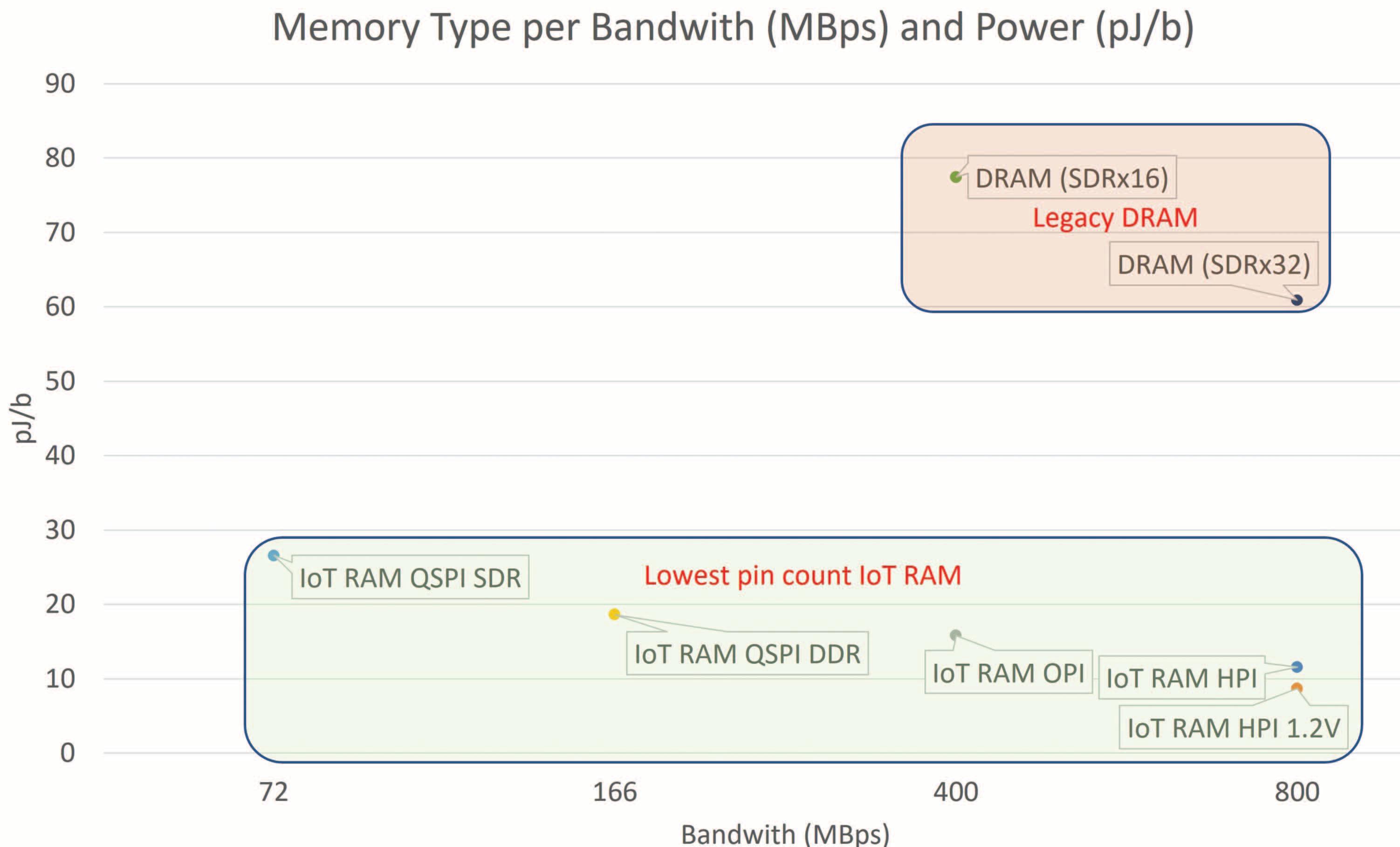
In terms of energy consumption, IoT RAM requires around four times less pJ/bit (picojoules per bit) than conventional DRAM (Figure 4). The short latency of IoT RAM enables fast power-up times and very fast wake-up from low-power modes and stand-by mode. Furthermore, IoT RAM offers full data retention with ultra-low standby power consumption –typically 0.1 to 0.3 μA/Mbit depending on density – as well as a deep power-down mode with less than 8 μA for all octal peripheral interface (OPI) densities.
The IoT RAM memories from AP Memory are based on PSRAM technology and already work with many MCUs, SoCs, and FPGAs that are widely used in IoT and embedded devices.

For a smart wristband, the required data throughput is calculated to be roughly 5 MB/s (71,392 × 3 bytes × 30 fps). Considering the additional latency for the SoC bus and the choice of memory bus frequency of less than 100 MHz for many SoCs in this category, IoT RAM QSPI SDR is sufficient to achieve the required data rate.
With a simple smartwatch, on the other hand, the required data throughput of roughly 25 MB/s (135,424 × 3 bytes × 60 fps) is well above that and can even be higher depending on the actual model. In this case, IoT RAM OPI or HPI achieves the necessary data rate better.
For high-volume, competitive wearables, the WLCSP package options are recommended. IoT RAM with a wide range of bandwidths is also available for the smart home and industrial market.
For example, an entry-level 16 MB QSPI SDR-SOP8 IoT RAM is suitable for a simple thermostat display that requires about 10 MB/s. The high requirements of an HD 720p display, on the other hand, can be met with a 256 MB OPI or HPI IoT RAM in a BGA24 package.
IoT RAM
Turning point for many MCU-based applications


These features have made IoT RAM the memory of choice for wearables in recent years. Many of the latest MCUs, wireless SoCs, and FPGAs from market-leading manufacturers view this memory as the ideal choice for all IoT, edge AI, and industrial applications.

Bandwidth and power consumption of different types of memory.
Using reference designs from SoC partners and Rutronik, manufacturers can ensure the effective use of their developer resources and a short time to market for their projects.
Rutronik’s RDK2, for example, is based on Infineon’s PSoC 62 and, in combination with external PSRAM (64 Mbit QSPI), offers a modern and easy-to-use hardware platform for developing numerous applications, most notably wearables and sensors.

Summary
Low pin count, low power consumption, a wide choice of packages, as well as competitiveness and simplicity in design, and integration of IoT RAMs make the real difference compared to conventional and legacy SDRAM approaches.
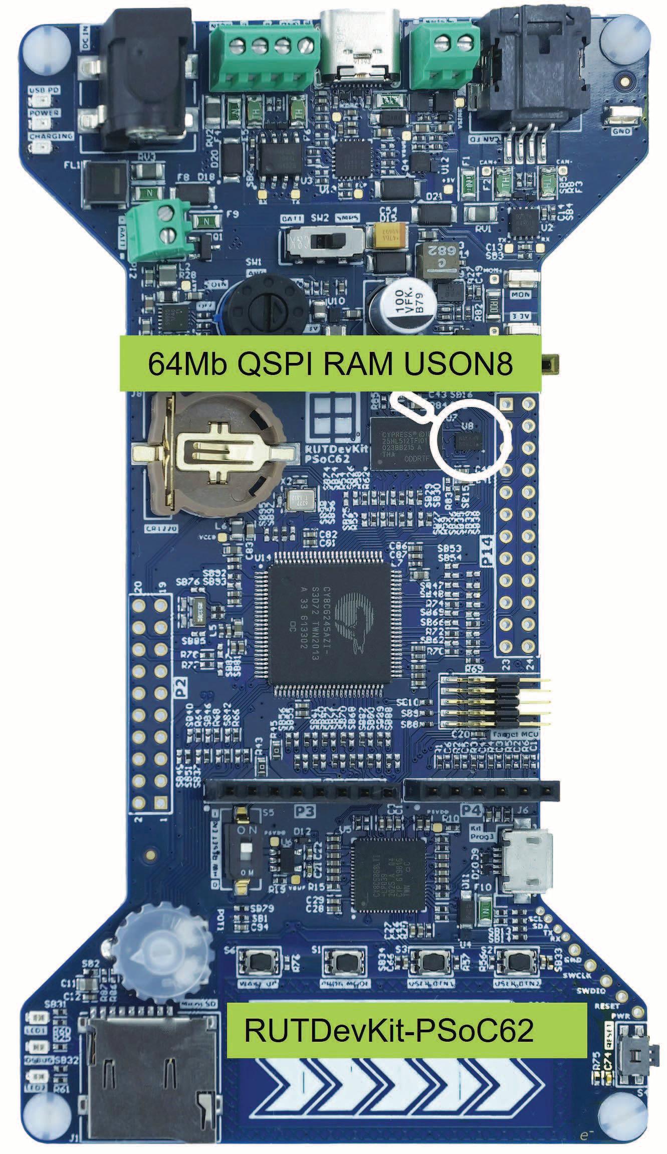
Using external IoT RAM, RDK2 is a modern and easy-to-use hardware platform, especially for the development of wearables and sensors.

Figure 6
Examples of image storage requirements for varying applications.


The future of agriculture is on the horizon – one where technology will be leveraged to provide greater control over nearly every aspect of the growing process and beyond. These technologies, including automation, artificial intelligence (AI) and machine learning (ML) make precision farming a reality by generating new insights and enabling cutting-edge capabilities that haven’t been possible with traditional agriculture processes.
Author: Josh Mickolio Supplier
Now, with new information in hand, growers and farmers can dig deeper and understand exactly how to get the highest quality yield from each species they work with, all while using less energy and resources than previously needed. This is sustainable farming brought to life to better support and cater to our changing planet.
When agriculture stakeholders embrace and harness emerging technology to create true connectivity across the growing and food distribution processes, they’ll not only overcome many of their current challenges, but every decision they make will be outcome-based as well. Growers and farmers aren’t looking for or in need of new solutions that simply sound exciting or end up creating more work for them; they need real-world systems that solve their real-world problems, and fortunately, there are technologies readily available that help with exactly that.
The agriculture industry has been navigating the same issues as other industries in recent years – and then some. As inflation rises, farmland could be hit with long-term rates that alter purchasing decisions; ongoing supply chain challenges are impacting the availability of critical components needed to keep equipment running smoothly; and up-for-debate farming policies could influence future food pricing.
However, there are other deep-rooted challenges within the industry as well –challenges that not only impact growers, farmers, and their partners and suppliers, but the world at large:
• Population growth: In November 2022, the global population reached eight billion, only 11 years after surpassing seven billion. It was reported that much of the growth (70%) has come from low- and lower-middle-income countries, where the growth trend is likely to become more pronounced in the years ahead. A rapidly growing population creates the need for more food and faster food production, yet many of these regions are also impacted by increasingly intense changes to their climates, which have negative implications on their ecosystems and, therefore, their food quality and security.
going out of temperature range because of a stalled shipment or faulty forecasting by retailers and restaurateurs that results in overordering. Unfortunately, this amount of wasted food could feed 1.26 billion people every year.
• Labor shortage: Steep machinery and technology investments, unpredictable and intense weather patterns, rising land prices and volatile pricing models are only a few reasons the younger generation has been reluctant to pursue careers in the agriculture industry. Today, farmers under 35 represent only 8% of all U.S. farmers, and there’s been a 52% decline in hired farmworkers as well. The labor shortage is intensifying just as the need for more and faster food production is rising.
Individual businesses are grappling with their own unique business challenges on a
• Food waste: What happens after food leaves the farm – tracking where it goes and how it gets there – is a step within the food distribution process that’s in need of serious attention. An estimated 30-40 percent of the U.S. food supply is wasted. This occurs for a variety of reasons, whether the food’s spoiled from
daily basis, but the implications of their choices and how they approach the future of their operations have an impact on everyone. In other words, the pressure is rising. Agriculture practices need refinement now in order to tackle the challenges of today and those we anticipate seeing years from now.
New solutions can reduce waste as well as the number of resources that are used and needed.


The agriculture industry is a proud, resourceful market where growers and farmers literally solve problems and experience success with their own two hands. They know their setup, they know their farms and they know the issues they’re facing. These stakeholders aren’t looking at technology as a silver bullet that can fix all their problems, though they are continuously thinking of new ways to address issues – and many are coming around to the idea that technology can aid and ease their efforts. When it comes to reducing waste and implementing more sustainable practices, it can feel counterintuitive to introduce more. Electronics, especially, aren’t the first thing that comes to mind when approaching sustainability.
Yet, if used properly, new solutions can reduce waste as well as the number of resources that are used and needed, bringing more sustainable, efficient options to light for food production. Technology can create a digital thread from the farm to the end user, which is not only desired today but required for both food safety and security and business resiliency.
For example, as our population grows, one of the easiest ways to make up for it is to reduce waste in the products that are already being created and shipped.
shipment of food to track temperature, position and location and share that information and any potential changes to the shipment in real time. This creates a better sense of connectivity throughout the entire process; stakeholders know when food leaves the farm and when it arrives at its end destination as well as anything that occurs in between, which helps inform and refine the shipment process to reduce spoiled product and overall waste.
Forced to do more with fewer resources as the labor shortage holds strong, growers and farmers are adopting automation solutions that allow them to both sustain current operations and maintain the quality of their products. Semios, a precision-farming platform, implemented a remote monitoring solution throughout a vineyard in Italy to optimize its productivity. Grapes are a highly sensitive crop, so it's important for them to closely track and monitor soil moisture and heat, especially as many growers are starting to experience changing climate conditions that impact their crops. With a network of sensors from Semios, vineyard growers can keep an eye on their whole field without any manual monitoring (i.e, sending someone out to take notes). This provides an extra layer of visibility into their operation that didn't exist before, while also maintaining (or even reducing) the same number of workers needed to monitor the grapes. Digitizing the farm and beyond is well underway for many agriculture stakeholders, and it’s starting to bring to life an industry that’s more capable and connected than ever before.

For example, instead of managing extensive farmland, vertical farming takes growing down to a much smaller space, where all the nutrients, resources and light that are needed for the crop are provided in a controlled area. Growers are able to detect patterns using advanced AI and ML technology to ensure the crop only receives as much light and water as needed to maximize and optimize the yield.

Miravel, a company that designs automated indoor wall gardens, has developed small packs full of seeds, nutrients and anything else needed for growing herbs and produce, and they install the packs in racks that are then pushed into a vertical farm. Each rack has sensors for moisture, temperature and light that tell a story about the growth of the plant; then, when more water is needed, there are automated water pumps that feed the rack. It’s a truly connected system that operates on real-time data with an output that’s sustainable, safe and high quality.
There are technologies now that can better monitor food through the supply chain to prevent excess waste. Airgain, a provider of wireless connectivity solutions, leverages wireless cellular modems to connect, monitor and control various touch points within an operation. They can implant tracking devices on a
Understanding what’s occurring at the ground level – hearing from the farmers themselves – helps to provide a sense of what daily operations are like within everyday agriculture and how the methods in which food is produced impact the environment. Now, as food production scales, it’s time to dig deeper and look at the component level and how technology is currently being used today. New innovations in agtech, like advanced automated sensors, and new approaches to growing like vertical farming and industrial-sized indoor farms are quickly becoming integral to securing a future for the industry –and are undoubtedly helping growers and farmers rethink what’s possible.
Agriculture stakeholders – growers and farmers, their partners and suppliers –value their resources. They only want to use the water, nutrients and chemicals absolutely needed to keep their crops healthy and safe. They value the knowledge of knowing what the soil moisture should be and how different weather patterns can impact their crop. They’ve inherently always wanted to be precision growers and farmers because their resources are precious. Now, through connected sensors and networks, advanced algorithms and real-time visibility, they can bring precision, sustainable farming to life. Their operations can use less energy, reduce waste and be more efficient with the aid of modern solutions. The possibilities are endless –the future of agriculture is looking connected and greener than ever.
DigiKey is both the leader and continuous innovator in the high service distribution of electronic components and automation products worldwide, providing more than 14.9 million components from over 2,400 quality namebrand manufacturers.

 ■ DigiKey www.digikey.com
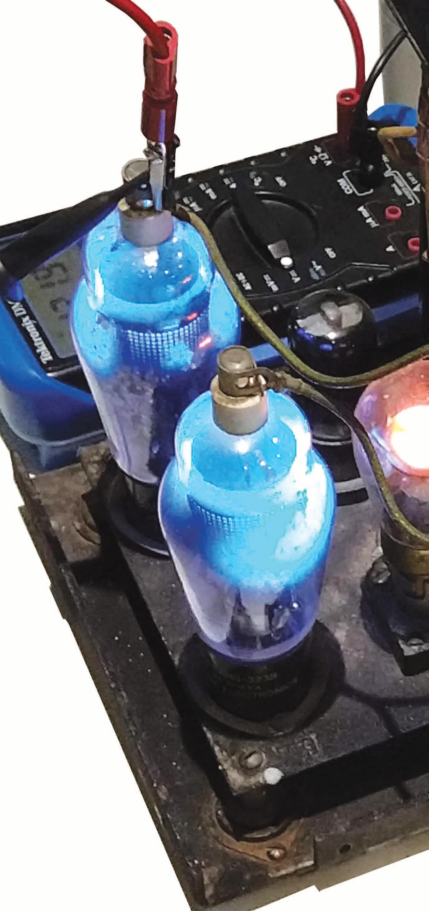
Celebrating my 40th year within power electronics, and as I presented at several Power Electronics conferences and papers, the history of the power industry is fascinating and one full of amazing, genius level engineers who are making power solutions more efficient, lighter, smarter and much more. Although it is difficult - if not impossible - to name all of them, one thing they all have in common is ‘curiosity’. For many of us Albert Einstein influenced our destiny and I cannot mention him without a quote, one that is also my own mantra: “The important thing is to not stop questioning. Curiosity has its own reason for existing.” This is the reason why for more than 120 years power designers have performed miracles and will continue to break ‘unbreakable limits’.
Autor: Patrick Le Fèvre Chief Marketing and Communication Officer Powerbox (PRBX)
The passion and curiosity for discovery
What makes a young guy decide to study power electronics depends on many factors but personally, I was probably influenced by the blue light emitted by a couple of thyratrons, when at the college in 1974, I visited the Paris “Palais de la découverte” and met a research engineer who in sharing his passion for electronics explained to me how that technology would change our future. It was just fascinating and almost certainly it was the day when my curiosity for discovery was born! For many power young engineers the word “thyratron” may suggest a time
when dinosaurs still walked the Earth, but for the power industry it was an important step forward in its time, and the state of the art (Figure 1).
We should also remember that at the same time as when the power electronics field was deploying electronic tubes, in 1926 the inventor Julius Edgar Lilienfeld patented the principle of what is today known as the Field Effect Transistor. In its patent: “Method and Apparatus for Controlling Electric Currents”, he proposed a three-electrode structure using a copper-sulfide semiconductor material. Julius Edgar’s research was very interesting but in com-
mon with many passionate research engineers he did not realize the importance of publishing and sharing results, making his discovery a case of debate within the research community and as a result low recognition for himself.
At this point it is pertinent to mention the high level of research undertaken to replace electronic tubes with something smaller, more efficient and easier to control. It is therefore relevant and only fair to mention Russell Ohl, who in 1930 experimented with the use of silicon rectifiers as radar detectors. This discovery was followed by an application for a patent of the photovoltaic principle (US Patent 2,402,662) but Ohl’s discovery set up the foundation of what would become the transistor.
In 1947, John Bardeen and Walter Brattain experimented with the first semiconductor amplifier that they duly demonstrated
ment regarding the filing of a patent in June 17, 1948 (2,524,035) and a couple of weeks later at a press conference in New York on June 30, the announcement of the ‘transistor’ by electrical engineer John Pierce. We all know the story and have seen the cover page of the September 1948 edition of the magazine ‘Electronics’.
From electronic tube to silicon


The invention of the transistor has been a real revolution, and was implemented in the early fifties in consumer equipment e.g. the transistor radio (1954, the Regency TR-1 in USA ; 1955 the TR-52 from Sony in Japan). Germanium transistors became the norm and power electronics engineers started to develop power solutions based on that technology. In parallel the growing demand from the scientificcomputer community to get faster machines boosted the development of a new generation of transistors based on silicon. In July 1961, the first NPN silicon transistor to exceed germanium transistors’ speed was released by Fairchild Semiconductor – the 2N709.

The launch of the silicon-based transistor accelerated the development of modern power electronics and what we know today as ‘linear regulated’ power supplies (AC/AC transformer, rectifier, analog regulator

power supplies based on ‘switching technology’. Although it was very confidential at the time, it was later reported that the technology was used in 1962 in the Telstar satellite.
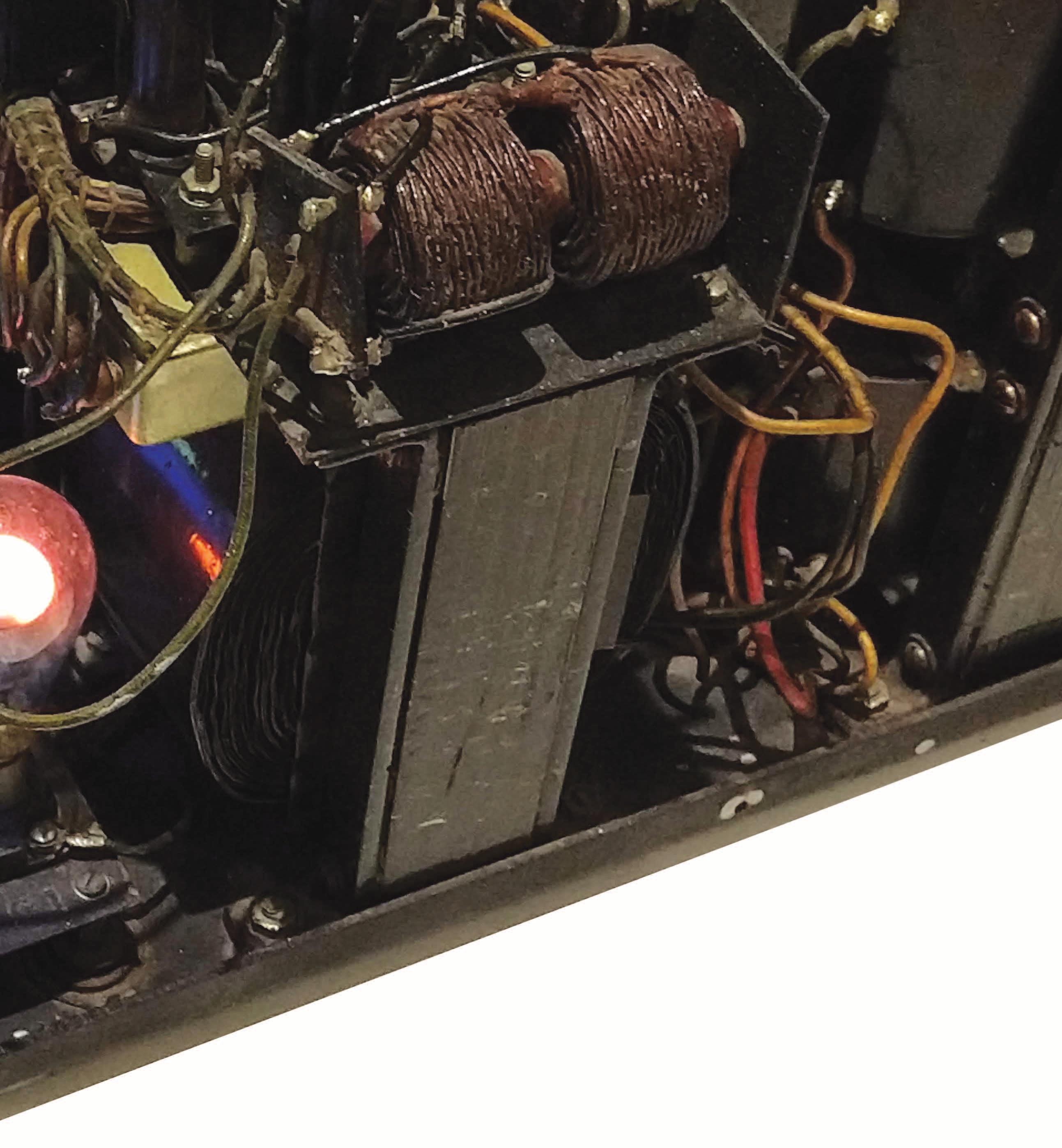

Who launched the first commercial switching power supply is up for debate, but we should mention RO Associates who in 1967 introduced a 20Khz power switcher, followed by Robert Boschert who in 1970 performed research on modern switching topologies. Boschert applied for a number of patents but the two most well-known are 4,037,271 and 4,061,931 that were granted in 1977. From that date the development of switching power topologies accelerated and with the introduction of MOSFET semiconductors and the PWM control IC it became the norm.
Because power supplies are used in applications ranging from deep sea to deep space, power designers face many challenges, some of which seem to be almost impossible.
Regulations and consumer demand for smaller and lighter equipment placed a high demand on power designers to increase efficiency. In the eighties, with high levels of curiosity, power designers explored high frequency switching resonant topologies and one of the most commercial success stories is Vicor, founded by Patrizio Vinciarelli in 1981.
At the same time the hard-switching community explored a new path, replacing diodes with power MOSFETs and here to mention the impressive work from Siliconix inviting, in 1984, more than 30 power electronics engineers to contribute to a Master Handbook which created a lot of attention within the power electronics community (Figure 2). In this move, from linear-power to switching-power, papers were presented at many conferences, e.g. PESC-1988, APEC-1989 but one of the main architect of market adoption is definitely James Blanc from Siliconix Inc. who with both passion and enthusiasm promoted synchronous rectification technology.
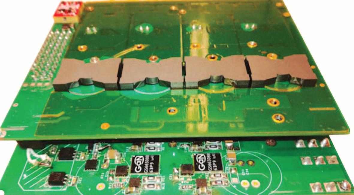
New components and topologies made power supplies more efficient, and trail blazed by Trey Burns, Chris Henze and the others who in the late seventies worked tirelessly to develop digital control of power supplies. It took several years to move from research to commercial implementation and it was in 2000 that power designers and semiconductor manufacturers finally broke a new ‘unbreakable’ limit.
‘Digital Power’ was born and it was now possible to control ‘bit-by-bit’ the performance of a power supply.
But the power designers’ curiosity is strong and unceasing, and with the market demand for even smaller components and greater efficiency, they are now busy exploring out of the silicon box, researching new materials with higher performance levels, the so call Wide Band Gap (WBG) semiconductors. In that respect, high voltage applications have gained benefits firstly from the use of Silicon-Carbide, followed by GalliumNitride (Figure 3).
What is amazing with WBG is the rapid take up of the technology in commercial applications. Earlier I mentioned James Blanc who for years promoted the use of synchronous rectification.
With that same level of passion I should now mention Alex Lidow (Efficient Power Conversion) who has strongly advocated in favor of WBG semiconductors and especially Gallium Nitride (GaN), making this technology easy to learn and fun to implement (Figure 4).

Every decade has witnessed major steps forward in reducing energy consumption, weight, space, and price.
Combining all of those, power designers have squeezed more power into smaller spaces and for example we all see the benefit in the latest generation of USB chargers. Year after year we get ever closer to the mythical 99.99% efficiency and that is the result of genius level power designers who are curious and never stop asking questions.
At the beginning of this article I quoted Albert Einstein, and so it’s relevant to end with him saying:
“The important thing is to not stop questioning. Curiosity has its own reason for existing. One cannot help but be in awe when one contemplates the mysteries of eternity, of life, of the marvelous structure of reality. It is enough if one tries to comprehend only a little of this mystery every day.”
This is what power designers have done for centuries and what is motivating all of use to break ‘the unbreakable limits’.
■ PowerBox www.prbx.com
Figure 3
References
Powerbox (PRBX): https://www.prbx.com
CuriousMarc - REC-30 Thyratron power supply for 1940 Teletype: https://youtu.be/WX74GoHuwHk Efficient Power Conversion (EPC): https://epc-co.com/epc


This article highlights how FPGAs are enabling the next generation technology revolution by offering power-efficient performance in many new high-volume applications in every walk of life. Small form-factor cameras running AI algorithms are guiding farmers via drone images, providing video analytics in retail chains, counting passengers in transportation, and reading license plates in toll booths.
Miniaturization is a key feature in most embedded systems today. We want more computing power in our pockets. Most FPGA-based embedded systems are also following the same trend. We want smaller industrial and professional cameras, medical handhelds, smaller programmable logic controllers (PLCs) and driver assistance modules in cars.
Miniaturization also poses additional challenges – the biggest one can be condensed into a single term “power-efficient performance”. Typically, if a system’s performance goes up, its power consumption does too, which in-turn increases heat dissipation. And in smaller modules heat dissipation is a headache system that designers cope with every day. Cooling a module so that it can operate under a thermally-
constrained environment often becomes the bottleneck to performance. In medical, portable ultrasound machines are democratizing care delivery in the field. Endoscopes and surgical-assist smart glasses are providing much higher resolution images to doctors than ever before. Thermal imaging-based surveillance systems designed to protect borders against intruders are also becoming smarter. Generally deployed in remote locations, these systems must operate autonomously while staying hidden.
Amateur content creators are all the rage today, driving a need for FPGA-based streaming video converters, offering creators the option to convert 4K video streams between any format like HDMI, SDI, USB or PCIe.
Industrial automation also benefits from the flexibility of FPGA-based architectures and the longevity of 20 plus years of Microchip FPGAs. Driver assistance systems in automotive keep the driver and passengers safe in our cars today. The FPGA architecture has come a long way. From choosing between performance and power, and only being used as a prototyping platform for expensive ASICs, FPGAs are now considered mainstream, offering highly reliable and cost optimized architectures, along with flexible and easy-to-use software.
Let’s have a look at various example usecases where PolarFire® FPGAs or PolarFire SoCs, with their hardened RISC-V processor-system, are playing a vital role.
Professional drones have strict requirements for flight safety:
• Accurate control and positioning, including collision avoidance
• Secured communication and control frequencies


• Predictable flying time
To be successful in a large drone market, drone manufacturers need to differentiate themselves by providing additional features such as high-resolution imaging and artificial intelligence. The drones often require multiple sensors, pre-processing or fusion of sensor-data and transferring that data via a wireless connection, making them complex systems. The application range is very wide and includes monitoring crop health and growth status in farming, object detection and potentially tracking in policing, military, or remote judgement in emergencysituations for fire departments or police. The flight control-electronics must be able to handle the motor-control and rotor speed, interact with sensors and link up with remote equipment, all in a size, weight and power constrained environment. A block-diagram for such a system can resemble the following:
Leveraging the flexible FPGA architecture, motors are driven by Field-Oriented Control (FOC) algorithms where control can be time-domain multiplexed because of the performance of the FPGA. Multiple motors are controlled by a common motor-control IP, with the exact number of motors depending on the chosen FPGA architecture.
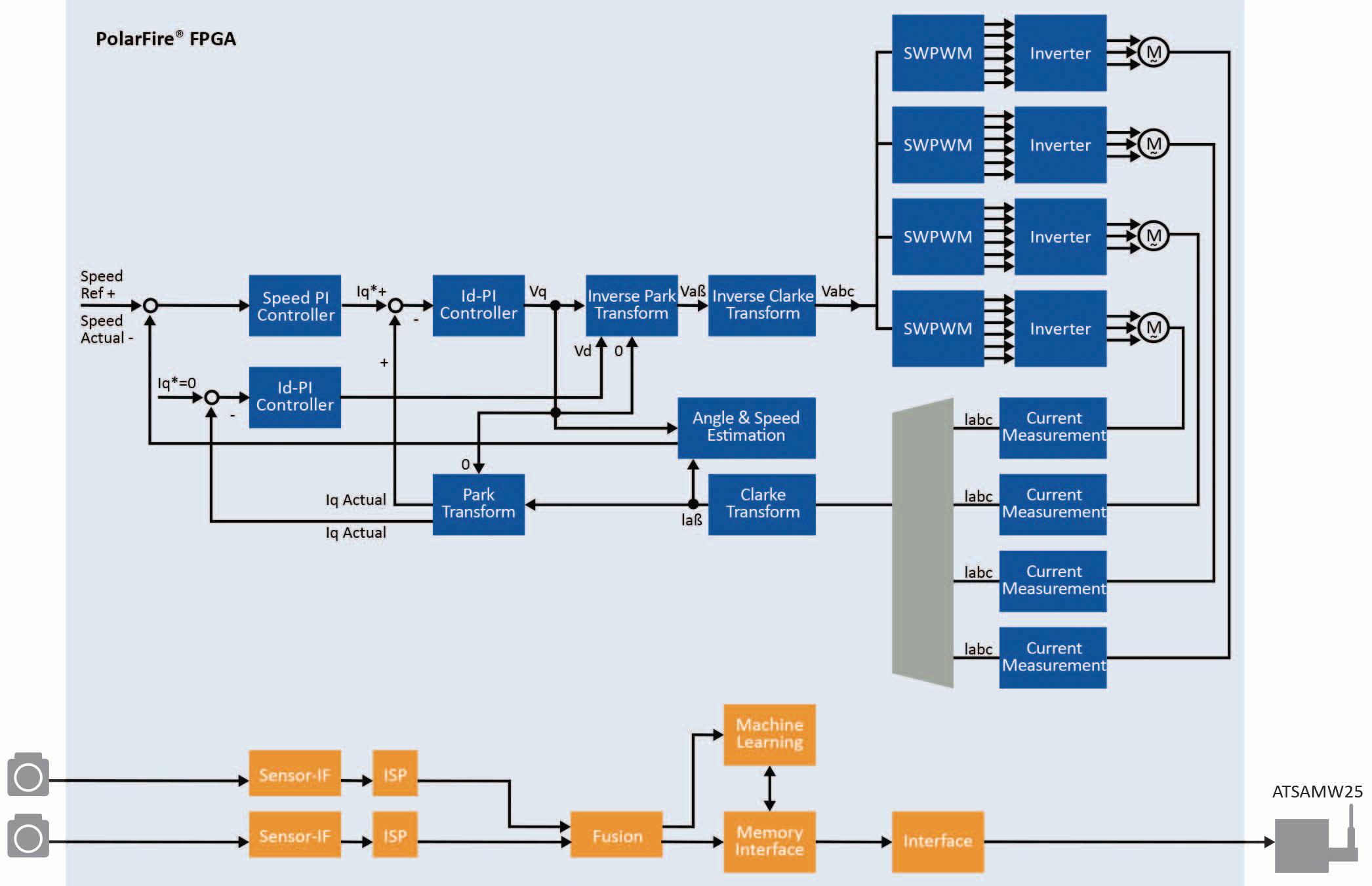
The high accuracy of the FOC allows a constant torque on the motors resulting in a smoother run with less vibration, less noise generation and most importantly extending flight time by approximately 10 percent or more compared to standard motor controllers using simple microcontrollers. Additional interfaces such as visual light, motion or infrared sensors used to support enhanced features such as machine vision need careful consideration, and historically required specialized expertise. Microchip’s VectorBlox™ SDK and matrix processer IP helps novice FPGA developers to deploy complex neural network algorithms in the FPGA fabric. This allows classifications or detections at a very lowpower footprint. The neural networks running on this accelerator-IP are designed using standard frameworks like TensorFlow or Caffe.
All results are buffered in local on-board memory and afterwards transferred to an on-board wireless module. This communicates with the operator where the collected data is received for storage and further use. The best-in-class security features of PolarFire devices protect both the transferred data and the drone itself from unauthorized access.
With complex drone architecture needing multiple application domains – motor control, flight control and imaging, using an FPGA provides the benefit of the individual “tasks” running in parallel.
Professional drone systems typically need to operate on a tight power-budget of 5 Watts or less. Using a PolarFire FPGA to manage multiple applications, power consumption of less than 1.5 W for the FPGA, including the operation of the neural network, is expected.
Due to the drive to miniaturize, coupled with power-efficient edge compute resources and enhanced thermal considerations, low-power medical imaging innovation is growing by leaps and bounds.
Leading the way are point-of-care diagnostics such as portable ultrasound equipment, consisting of a hand-held transducer, reading and sending sonographic data to a standard smart phone. Transmissions can happen with a simple cable or wirelessly. These systems are revolutionizing and democratizing diagnostic capabilities for emergency medical personal at incident sites, in less developed regions, and helping medical professionals make diagnostic decisions outside traditional hospital environments.
The following block diagram shows an example implementation (Figure 2).
Leveraging a PolarFire FPGA in a handheld medical device delivers the lowest total system power, which leads to efficient thermals, and keeps the transducer head cool allowing direct skin contact. These efficiencies extend operation time in a compact package footprint of only 11×11 mm² supporting very small probe enclosures.
Another area where flexibility paired with low power consumption and a small physical footprint is essential is the realm of video converters. High-performance professional cameras typically provide a single data interface, limiting post-processing equipment selections that support that specific interface. Having a video converter provide a bridge to several interface standards allows flexibility in selecting postprocessing equipment. Performance is not compromised as multi-protocols are supported with numerous multi-gigabit transceivers, and optimized line-rates of up to 12.7 Gbps, supporting HDMI, CoaXPress, SDI, and Ethernet protocols.
The converters form factors are compact as heatsinks and fans are no longer required. Video converters built on PolarFire technology are estimated to require less than two Watts of power consumption.
Here is a video converter design example:
consumption allows the device to remain cool enhancing thermal management design considerations. Resolution is not compromised, image-data of up to 4K with 60 frames/second can be easily handled with MIPI CSI-2 receiver-interfaces natively supporting up to 1.5 Gbps/line.
Two different use-cases are used as examples, industrial cameras and PLCs. Industrial cameras typically require high frame-rates, high resolution and a small form-factor which make the thermal design often a challenge. Thanks to the optimized package-layout, and efficient thermal characteristics, this challenge can easily be tackled. The low static power-

Even though it is physically larger as a complete system, PLCs are similarly space and power-constrained as cameras.
These rack-based systems are modular allowing end users to customize their system and offering standard chassis widths. Processing performance is still a must to support industrial ethernet, human machine interfaces, motor/driver control and Real-Time Operating Systems (RTOS).

The following graphic shows a generic block diagram of such a system, mapped to PolarFire SoC, the first FPGA-SoC built on a quad-core RISC-V processor. The PolarFire SoC supports asymmetric multiprocessing (AMP) natively, together with a fixed, fine-granular allocation of cacheways to individual processors.
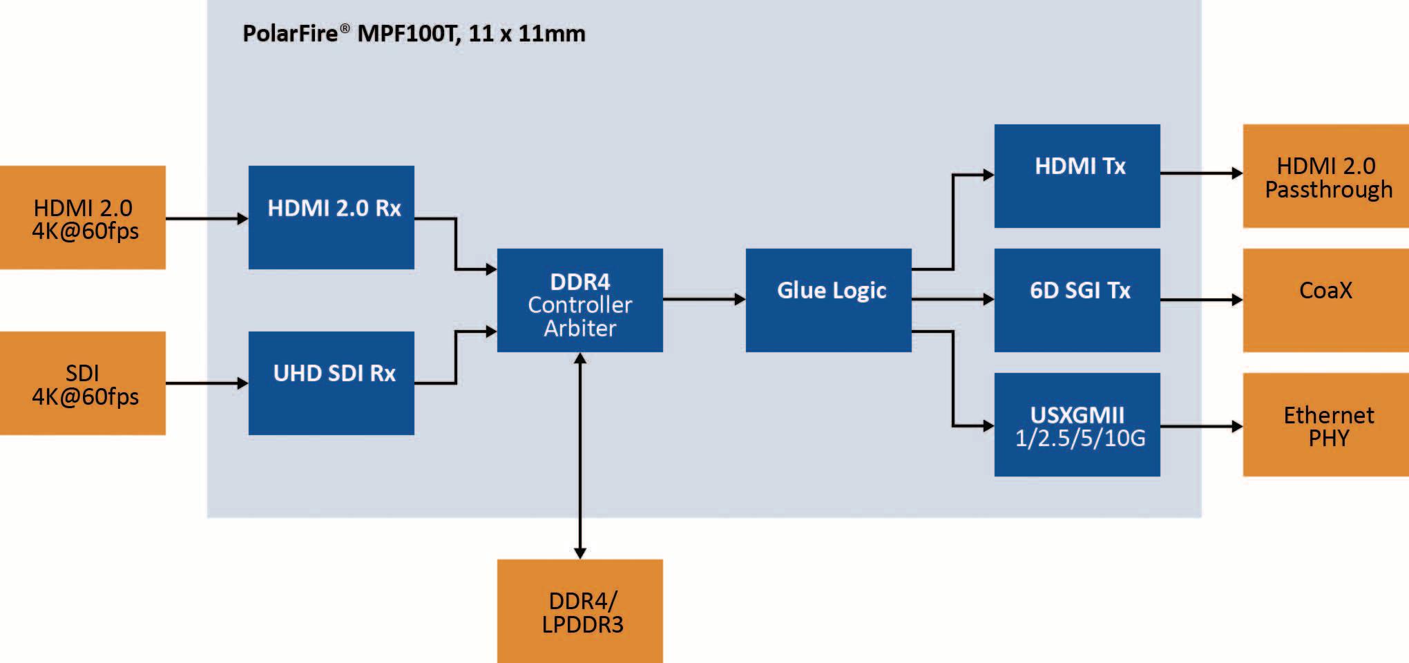
This native AMP support allows for multitasking. As an example, a single processorcore can be allocated for an industrial ethernet protocol stack, while a second core can be running a Linux operating system.
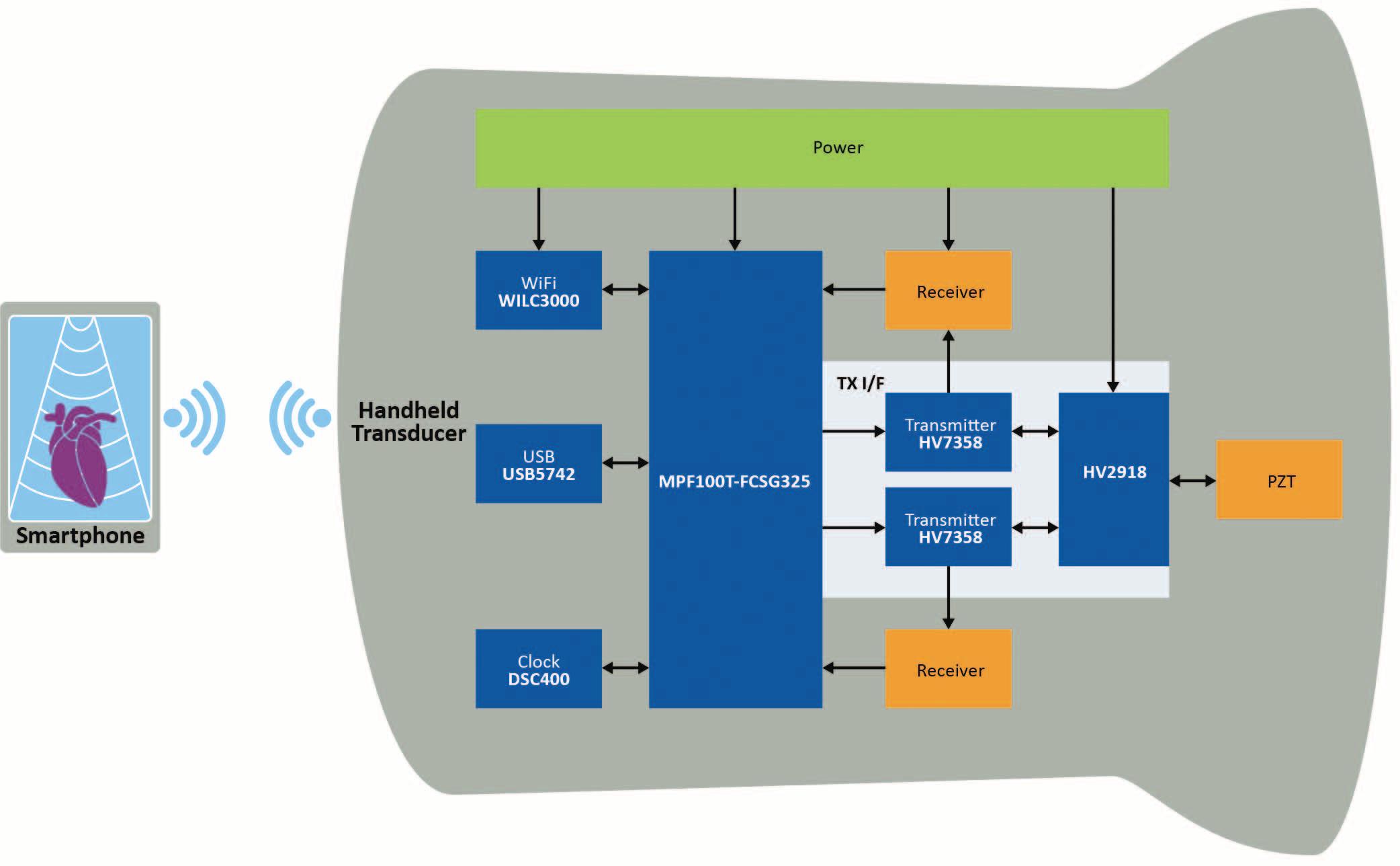
The corresponding cache is fixed, and Linux is being separated from other hardware-resources. Additionally, the other two available cores can be used to handle the required algorithms for motor control or an inverter (Figure 4).
These cameras allow the detection of dangerous situations with feedback to the driver or also with direct control into the vehicle like automatically activating the brakes. These systems have strong requirements for functional safety, security,
The received image frames are processed in streaming mode using the parallel nature of the FPGA and additionally provisioned with additional safety information like frame-count and CRC for end-to-end protection of the communication. The streaming processing of the image-data avoids the danger of using “frozen images” from memory and allows processing with fixed execution time, directly translating into more time for the system to react. Depending on the exact OEM-requirement, the FPGA also provides the required flexibility to support interfacing to various established proprietary serializers.

Common to all applications, yet not detailed above, are the business drivers for bringing a successful product to market. Looking at how to reduce risk, while reaching the client ahead of your competition, and optimizing system-cost while delivering profits to the bottom line requires careful consideration of your system architecture and supply partner.
Again, low power consumption plays an important role keeping the temperature of the electronic components inside the blade modules low, even in challenging thermal environments of 60°C ambient temperature and more.
For a closer look on why low power consumption is important in systems that are cable-powered, please refer to the following article, hosted on the Microchip blogs
Industrial automation spans a wide range of applications and requirements. Common amongst industrial products is a need to offer support and availability of devices for 20 years or more. Microchip is fully dedicated to this longevity requirement and offers support with a robust “assurance of supply” program.
Many different applications in today’s automotive market require the flexibility of FPGAs, ranging from sensors like LIDAR, imaging radar or cameras to more hidden functionality like highly accurate and closely synchronized driving of electric motors via high-voltage drivers. A strongly emerging application is the use of cameras for collision warning.

and low-latency processing combined with the capability to operate reliably in high temperature environments caused by engine heat and sunlight.
The following diagram shows a system setup using the PolarFire MPF050T, safety elements are drawn in yellow, security in green (Figure 5).
The integrated secure non-volatile memory (sNVM) allows the storage of fleet-keys to authenticate within the camera module within the vehicle-network.

The comprehensive Microchip portfolio offers a total system solution partnership. Benefit from key components and reference design solutions to reduce development risk and component counts. Designers can also save time and money as solutions are validated for cross functionality and offer warranties in many cases.
For further information click here


■ Microchip Technology www.microchip.com


the company’s MEMS hydrogen sensor tech nology, the new PGS4100 hydrogen sensors accurately detect hydrogen concentration in the air by measuring the change in thermal conductivity of the gas mixture within BMS compartments. This technology enables faster reaction times for triggering battery failure alarms in electric vehicles (EVs), ensuring compliance with safety standards.
The PGS4100 series is designed with a relative humidity sensor and a barometric pressure sensor. This strategic incorporation enables the sensor to counterbalance thermal conductivity changes influenced by humidity in air and elevation changes, enhancing the accuracy of hydrogen concentration measurement. This level of precision enables the PGS4100 to meet industry standards for flammable gas detection.
Built around Posifa’s second-generation thermal conductivity die and packaged in an SMD form factor, the PGS4100 operates using a pulsed waveform. This design approach ensures the sensor’s heater temperature aligns closely with the ambient temperature, thereby ensuring intrinsic safety.
The PGS4100 series supports analog voltage and I2C digital outputs, with future models slated to support MODBUS/UART and CAN bus. Encased in an IP6K9 compliant enclosure and equipped with a wire harness terminated with an automotive-grade connector, the PGS4100 series exemplifies durability.
Key features of the PGS4100 series include compensation for humidity and pressure, ensuring accurate functioning in harsh environments. Notably, the sensor remains non-reactive to “poisons” or contaminants, guaranteeing longterm stability and reliable performance.
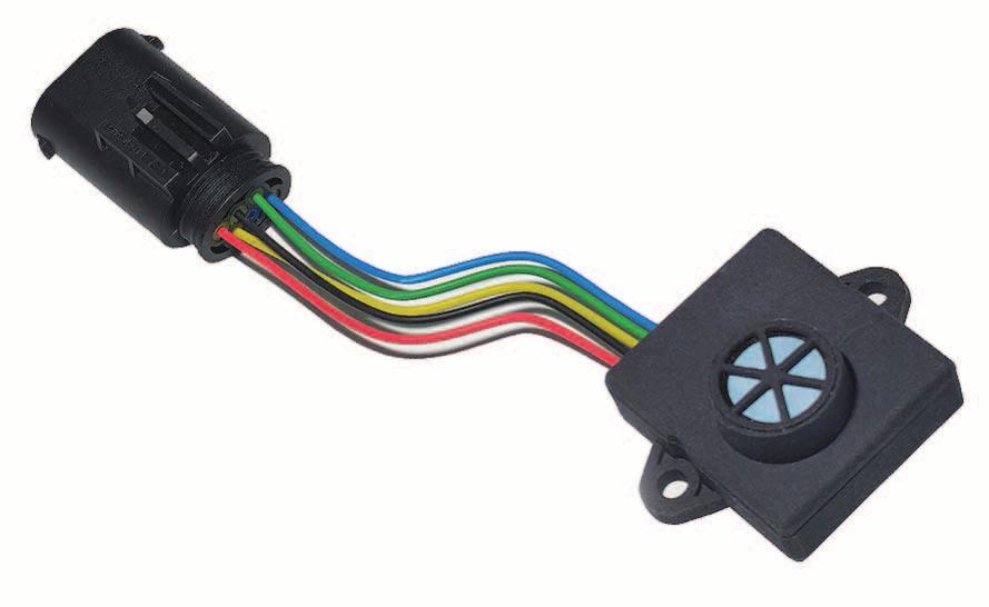
Further information about the PGS4100 series hydrogen sensors is available at https://posifatech.com/pgs4100/
■ Posifa Technologies

https://posifatech.com
Renesas Electronics Corporation announced that its automotive cybersecurity management system (CSMS) used for the development of microcontrollers (MCU) and system on chips (SoCs) has been defined and implemented according to International Standard ISO/SAE 21434: 2021. The CSMS framework applies to Renesas’ design center in Musashi, Japan and has been certified by TÜV Rheinland Industrie Service GmbH according to the following.
• Automotive CS Management (TÜV Rheinland)


• ISO/SAE 21434 – Automotive Tier Supplier
• ACSM (Automotive Cyber Security Management) 112: ML2: Managed

The certification reaffirms Renesas’ commitment to customers and original equipment manufacturers (OEMs) that Renesas will continue to meet its CSMS responsibilities and help car manufacturers obtain vehicle type approval as part of the recent UN Economic Commission for Europe (UNECE) UNR155 regulation. As indicated in an earlier press release, all Renesas automotive MCUs and SoCs which were developed after January 1, 2022, will sequentially follow this certified ISO/SAE 21434:2021 Cyber Security Management System (CSMS) development process. This includes the company’s 16-bit RL78 and 32-bit RH850 MCUs as well as its popular R-Car SoC Family.
“With this certification, validated by an independent third party, customers can have confidence that our management of the CSMS process is meeting the requirements defined by ISO/SAE 21434:2021,” said Takashi Yasumasu, Vice President of the HPC Core Technology Division at Renesas. “OEMs and Tier1 suppliers can simplify their vehicle type approval process by utilizing this independent third-party certification, instead of conducting their own audits of our process.”
Renesas has made significant contributions globally to the development of the ISO/SAE 21434:2021 standard. Renesas’ commitment and dedication to cybersecurity extend beyond the automotive industry. In 2019, Renesas was certified by TÜV Rheinland as compliant with the IEC 62443-4-1 standard, which specifies the process requirements for secure development of industrial products. Renesas continues to develop safe and secure products for its customers. ISO/SAE 21434:2021 certification is the latest addition to Renesas’ achievements, following the company’s long history of ISO 26262 compliance on automotive MCUs and SoCs. Customers can be confident that when using Renesas MCUs and SoCs for next-generation automotive systems, they are complying with international standards in product cybersecurity and functional safety. For more information, please visit:
https://www.renesas.com/application/automotive/automotive-security ■ Renesas Electronics Corporation | www.renesas.com


Renesas Electronics announced a complete space-ready reference design for the AMD Versal™ adaptive system-on-chip (SoC) XQRVC1902. Developed in collaboration with AMD, the ISLVERSALDEMO2Z reference design integrates key radiationhardened components for power management, including four new and recently released products in an ultra-compact design. These Intersil-brand ICs are specifically designed to support a wide range of power rails for next-generation space avionics systems that demand tight voltage tolerances, high current, and efficient power conversion while withstanding the harsh environment of space.
As core voltages decrease and currents increase for FPGAs and ASICs, it has become more difficult to meet the stringent power requirements of these devices to ensure that they operate errorfree. This is especially critical in space missions where power availability is limited, and systems are exposed to extreme temperatures and radiation for an extended period of time.
To address these challenges, Renesas has collaborated with AMD to develop a complete power management solution for the AMD Versal platform. The Versal Adaptive SoC is an industry-leading space-grade compute platform that delivers full radiation tolerance, accelerated AI inference and high-bandwidth signal processing performance. The ISLVERSALDE-
MO2Z generates each of the power rails utilized by the Versal platform, including a low 0.80V core voltage supply that can source up to 140 A (amps) of current. Renesas’ new reference design comes with an array of power management devices that have been tested and verified to withstand exposure to high levels of radiation. These include Pulse Width Modulation (PWM) controllers, GaN FET half-bridge drivers, point-of-load (POL) regulators, power and enable switches, and power sequencers. The devices come in small-footprint packages, so the core power rail components take up just 104 square centimeters of board area, approximately equivalent to two business cards.


SL73847SEH Rad-Hard Dual Output PWM Controller
• Synchronous buck controller
• Single- or Dual-phase
• 4.5V to 19V input voltage range
• Output voltage as low as VREF: 0.6V+/0.67% (temperature, radiation and life)
• Differential remote sensing of output voltage
• Radiation tolerant, LDR (0.01 rad(Si)/s): 75krad(Si)
• Operating range: -55 °C to +125 °C
ISL73041SEH and ISL71441M: World’s First Dedicated Gan FET Half-Bridge Drivers for Space Applications
• Interfaces with ISL73847SEH synchronous buck controller
• Programmable gate drive, 4.5V to 5.5V
• Bi-directional communications with ISL73847SEH for start up synchronization and fault detection.
• Highly matched, fast propagation delays between high- and low-side drivers
• Wide VDD input voltage range, up to 13.2V
• Best-in-class Single Event Effects (SEE) performance
• Available in ceramic (ISL73041SEH) or plastic packaging (ISL71441M)
• Operating range: -55 °C to +125 °C
ISL73007SEH Rad-Hard POL Regulator
• 3V to 18V input voltage range
• Internal or external loop compensation 1% reference voltage over temperature and radiation

• Efficiency ≥90% from 1A to 3A
• Industry’s smallest footprint in 14 lead ceramic dual flatpack package

• Radiation tolerant, LDR (0.01rad(Si)/s): 75krad(Si)
• Operating range: -55 °C to +125 °C
All products are available today and the reference design is available upon request in limited quantities. Please contact a sales team for more information or visit the Renesas website.
Renesas Electronics Corporation
www.renesas.com

Vicor, a leader in high performance power modules, releases its new e-book detailing the innovation needed to manage high power demands across the aerospace, defence and satellite sectors.
The new e-book – ‘Innovative and reliable power solutions for mission critical applications’ – highlights case studies and technical articles to provide readers with in-depth knowledge and application-specific insights into designing better power delivery networks.

As space exploration grows exponentially and governments continue to invest heavily in defence spending, this sector is seeing higher demand for innovative and reliable power solutions.
For example, high-performance LEO and MEO communications satellites require compact power solutions that are radiation-tolerant to survive the harsh environment of space. Satellite operators are offering increasingly more sophisticated on-board processing capabilities necessitating the use of the latest ultra deep submicron FPGAs and ASICs.
These have demanding, low-voltage, high-current, power requirements and OEMs are being challenged to offer more functionality from smaller payloads and platforms. Additionally, as electronic systems are becoming more standardised in defence applications, there is a demand for increased interoperability, scalability and reliability.
Size, weight and power (SWaP) are always target parameters in aerospace and defense applications and this will remain the focus. From the requirement for high density solutions in UAVs to designing radiation-tolerant power electronic solutions, Vicor’s lightweight compact high density power modules provide flexibility for power system designers.
The new e-book examines a range of challenges and modular solutions. It presents technical advice using Vicor’s power modules and answers frequently asked questions about power – in this downloadable guide.
‘Innovative and reliable power solutions for mission critical applications’ addresses critical pain points within the aerospace, defence and satellite industries, including:
• Powering tethered, aerial and underwater vehicles

• Electronic countermeasures
• Delivering high power density and low noise for space applications
• Radiation tolerant power electronic systems
Scott Fowler, Business Development Manager, Aerospace, Defence and Satellite, Vicor, said, “OEMs are facing increasing pressure to find lightweight scalable solutions that can meet the applications power needs and this new ebook presents cases studies and solutions. Customers are at the heart of what we do, so we want to enable them to explore new ideas while offering practical solutions and technical advice to them in one place. Also our online resource library contains a variety of literature to support our customers, so we’re excited to be adding a new ebook to the mix to support power system designers.”
Vicor’s ebook is free to download.To learn more about Vicor’s solutions for the aerospace and defence markets, please visit: www.vicorpower.com/industries-andinnovations/aerospace-and-defense or for space and satellite, please visit: www.vicorpower.com/industries-andinnovations/leo-satellite.
■ Vicor Corporation


www.vicorpower.com


TE Connectivity (TE), a world leader in connectors and sensors, has been a driving force behind the new IEC 63171-7 international electrotechnical standard, helping Single Pair Ethernet (SPE) interconnect technology gain faster acceptance in the industry.
Under the new standard, SPE-M12 hybrid interfaces, which TE expects to launch later this year, will enable the reliability, durability and safety required in harsh industrial environments.
The technology will allow higher levels of power to be transmitted in production plants, and is a promising option for robotic systems, as well as servo and three-phase drives.
TE pushed for the standardization as a founding member of the SPE Industrial Partner Network, a global network of more than 50 organizations. Adopted in May 2023, the IEC 63171-7 standard has been met with broad approval throughout the industry and has already been implemented by trade associations and companies around the world. The IEC 63171-7 standard specifies hybrid interfaces with SPE and power contacts in the M12 format – both with screw locking and push-pull quick locking. The standard applies to shielded, free and fixed circular connectors for power and data transmission. SPE-M12 hybrid interfaces fit almost seamlessly into existing Ethernet infrastructures and help to enable simple plug-and-play connections. Separate pins for data and power transmission contribute to a higher performance.
The new hybrid connection standard is a further development of IEC 63171-6, which defines M8 hybrid connectors, but does not consider the well-known M12 industry standard used in IP65 and IP67 environments.
The new standard now accounts for SPE-M12 hybrid connectors for different applications with power classes from 8A to 16A and from 50V to 600V. While previous concepts with Power over Data Line (PoDL) are limited to 50 W, SPE-M12 hybrid connectors support powerful devices up to 11 kW and 16 A. In addition, the hybrid configuration of the IEC 63171-7 standard offers greater flexibility in network-based power distribution than a point-to-point connection such as PoDL. Thus, it is possible to distribute higher current levels to several cascaded power devices.
More information on TE Connectivity’s SPE-M12 hybrid connectors is available at https://www.te.com/usa-en/industries/automation-control/insights/single-pairethernet/spe.html?te_bu=Ind&te_type=pr&te_campaign=oth_glo_ind-othglobal-pr-spe-standard-7-release-pr-en_sma-3200_9&elqCampaignId=173923

■ TE Connectivity | www.te.com
TASKING presents the new TriCore Qualified C Library (QClib) for the VX toolset. This simplifies the development of automotive software with regard to functional safety. Software library qualification is important and required by functional safety standards because the library code is incorporated into the application and installed on the target device. A faulty library can jeopardize the functional safety of the application. Therefore, both a qualified compiler and a qualified C library must be used for the development of software that must meet functional safety requirements according to standards such as ISO 26262 or IEC 61508.
The TriCore Qualified C Library is a full-featured ISO C library that provides approximately 600 functions. Of these, about 200 functions are suitable for use in ASIL-D software, the remaining functions are qualified for use in lower level ASIL or QM software. This allows for easy integration of the library into existing projects, interfacing with third-party operating systems, and enables the use of printf-style debugging and logging.
The QClib comes with a safety manual in both human readable (pdf) and machine readable (ReqIF) format. The ReqIF format makes it possible to automatically import the guidelines from the safety manual into the user’s requirements management system. The structure of the ReqIF file is such that all safety requirements are uniquely identifiable and allows reuse and sharing of safety analyses performed by different development teams, as well as (partial) reuse of safety analyses performed on different versions of the QClib product.
Using the Qualified C Library reduces the cost and lead time of safety related software and reduces product liability risks. The library is specifically designed for use in embedded systems and is highly optimized in terms of code size, execution speed, and accuracy of mathematical functions.

Availability
TASKING TriCore Qualified C Library is available immediately. Further information under https://www.tasking.com/products/tricore-qualified-c-library
■ TASKING Germany GmbH | www.tasking.com
Mouser Electronics, Inc., the New Product Introduction (NPI) leader™ empowering innovation, has released a new eBook in collaboration with Renesas Electronics, exploring the use of artificial intelligence (AI) and machine learning (ML) to drive innovation in Industrial Internet of Things (IoT) applications.
In Bringing Intelligence to the Edge: Designing Industrial IoT Applications with TinyML, six thought leaders from Mouser and Renesas offer detailed insights on how machine learning can be used to improve the design of industrial IoT (IIoT) solutions. The eBook features eight articles covering topics including AI in IoT endpoints, vision AI processing, and endpoint AI in embedded vision applications.

The rapid advance of IoT technologies has improved productivity and quality of life both at home and in the workplace. For IIoT applications, the introduction of AI and ML will lead to new use cases and fundamentally change the way in which engineers design new solutions. The application of AI and ML is particularly promising for highly constrained environments, which is now known as TinyML. Increased use of AI in IIoT design will result in devices that are less reliant on external systems, allowing the devices to make decisions without outside input or assistance. TinyML will also empower IIoT devices to process large data sets, leading to increased efficiency and new applications.
The eBook includes quick links to a range of Renesas Electronics products, focusing on microcontrollers (MCUs) and microprocessors (MPUs). These include the RZ/V2L highprecision entry-level AI MPUs, the RA4E1 MCU group, which is targeted for connectivity and security, the RA6M3 MCU group, which is designed for low power and efficiency, and the RA4M3 MCU group, which provides a balance of performance and cost-effectiveness.
With almost 30,000 Renesas parts available to order, Mouser offers an ever-widening selection of the manufacturer’s newest products, from MCUs and MPUs to sensors and optoelectronics, all supported by a rich ecosystem of development tools and software.
To learn more about Renesas Electronics, visit https://eu.mouser.com/manufacturer/renesas/.
To read the new eBook, go to https://eu.mouser.com/news/renesas-ai/renesas-intelligence-edge-ebook.html#p=1.

■ Mouser Electronics | www.mouser.com
https://international.electronica-azi.ro


Mouser Electronics, Inc. offers an insightful Industrial resource center, providing a wealth of information about the cuttingedge technologies that are driving the modern industrial automation transformation. Mouser explores the advantages of predictive maintenance and machine learning on edge devices and digital twin simulations for engineering professionals, allowing them to increase efficiency and lower costs. By leveraging these technologies, designers can create more efficient and reliable automation systems for applications within IIoT, robotics, AR/VR, industrial networks and more.
Mouser’s extensive catalog of products, eBooks, articles and blogs makes it easy for engineers to discover the latest trends in industrial automation. Mouser evaluates the potential applications of these technologies, from warehouses and manufacturing facilities to automated processes, and provides innovative resources that enable users to take full advantage of these solutions.
Mouser stocks the industry’s widest selection of semiconductors and electronic components, including the following solutions for industrial automation applications:
• Fido5100 and Fido5200 real-time ethernet multiprotocol (REM) switches from Analog Devices Inc. are designed as programmable IEEE 802.3 10Mbps/100Mbps Ethernet Internet Protocol Version 6 (IPv6) and Internet Protocol Version 4 (IPv4) switches that support virtually any Layer 2 or Layer 3 protocol. These REM switches can be ready for network data operation in less than 4 ms to support fast startup and quick connect type network functionality.
• Cat6A industrial mini I/O connectors, by TE Connectivity, enable a fast and easy field installation solution for Ethernet connections in industrial applications, with automatic wire cutting for optimal transmission performance.
• Opta® micro programmable logic controller (PLC), from Arduino, are secure Industrial IoT devices designed to make automation projects more manageable and more powerful with computing power for real-time control, monitoring, and predictive maintenance applications.
• ESRP-PCS-ADAM6 intelligent I/O gateways, by Advantech, offer an efficient and reliable way of connecting edge devices to the cloud, with a powerful Linux OS, over 200 drivers, and real-time data transmission capabilities for optimization of factory management and energy monitoring. For the latest on solutions for industrial, visit https://resources.mouser.com/industrial.
■ Mouser Electronics | www.mouser.com
Toshiba Electronics Europe GmbH (“Toshiba”) announces the launch of twelve 650V silicon carbide (SiC) Schottky barrier diode (SBDs) based upon their latest 3rd generation technology. The new devices are specifically intended for use in efficiencycritical industrial equipment applications including switching power supplies, electric vehicle (EV) charging stations and photovoltaic (PV) inverters.
Known as the TRSxxx65H series, the new devices use new Schottky metal. The 3rd generation SiC SBDs chip optimizes the junction barrier Schottky (JBS) structure of the 2nd generation products, thereby lowering the electric field at the Schottky interface and reducing leakage current – delivering enhanced efficiency.
The 3rd generation devices achieve excellent low forward voltage (VF) of 1.2V (typ.). This represents a 17% reduction when compared to 2nd generation products. The new 3rd generation products have improved the trade-offs between VF and total capacitive charge (QC) which is typically 17nC for the TRS6E65H. Also, the VF and reverse current (IR) ratio is improved compared to 2nd generation products with the TRS6E65H achieving a typical IR value of 1.1μA. All of these improvements reduce power dissipation and contribute to higher levels of efficiency within end equipment.

Devices within the TRSxxx65H series are capable of forward DC currents (IF(DC)) up to 12A and square wave non-repetitive surge currents IFSM up to 640A. Seven of the new devices are housed in TO-220-2L packages while the remaining five are provided in compact and flat DFN8×8 SMD packages.
Volume shipments of the new devices start today.
Visit Toshiba’s website to learn more about the new TRSxxx65H series.
■ Toshiba Electronics Europe
https://toshiba.semicon-storage.com
The LAN8670/1/2 family of Ethernet PHYs simplifies architecture to connect low-speed devices into a standard Ethernet network
Automotive designers are looking to replace legacy gateway subsystems with technology that can migrate applications to an Ethernet network to easily access information from the edge to the cloud. To provide OEMs with automotive-qualified Ethernet solutions, Microchip Technology (Nasdaq: MCHP) announces its first automotive-qualified Ethernet PHYs. This family of 10BASE-T1S devices with AEC-Q100 Grade 1 qualification includes the LAN8670, LAN8671 and LAN8672
The LAN8670/1/2 10BASE-T1S Ethernet PHYs are functional safety ready and designed for use in ISO 26262 applications. These devices now make it possible to connect lowspeed devices that previously required their own communication systems into a standard Ethernet system in automotive applications.
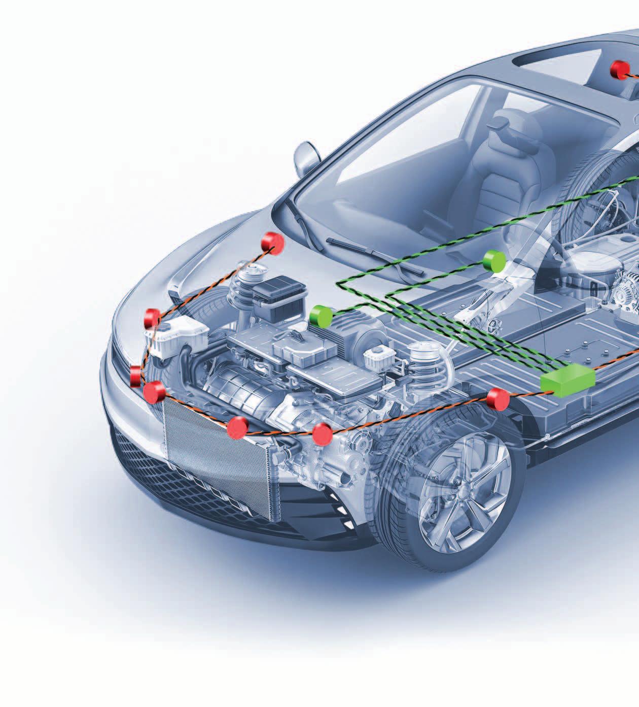
“Microchip continues to prioritize connectivity solutions for the automotive industry with the expansion of its line of 10BASE-T1S products,” said Matthias Kaestner, vice president of Microchip’s automotive products business unit.
“This new technology will connect the sensors and actuators used in the physical world all the way to the cloud, and it will enable a seamless Ethernet architecture everywhere.”
1.2V
The ability to connect multiple Ethernet PHYs to a common bus line makes it simpler to implement automotive applications on a single, well-known architecture and saves implementation costs by reducing cabling and switch ports. The LAN8670/1/2 enables the network edges to use Ethernet and Internet Protocol (IP) to easily communicate with the rest of the network infrastructure. These devices include advanced PHY diagnostics to provide the user with troubleshooting capabilities. In addition, sleep/wake functionality allows for low-power modes.
The 10BASE-T1S device specifications include 10 Mbps, halfduplex mode, flexible topology with multidrop bus line and point-to-point and use a single balanced pair of conductors. These devices also feature enhanced electromagnetic compatibility/electromagnetic interference (EMC/EMI) performance. Time-Sensitive Networking (TSN) support allows for synchronized timing across far-reaching Ethernet networks. Time synchronization is critical for many applications throughout automotive zonal architectures.
Microchip was a key contributor in the development of the standards with IEEE for the automotive-qualified 10BASE-T1S technology. This technology simplifies system design by expanding the reach of Ethernet to the devices that are typically at the very edge of the network.
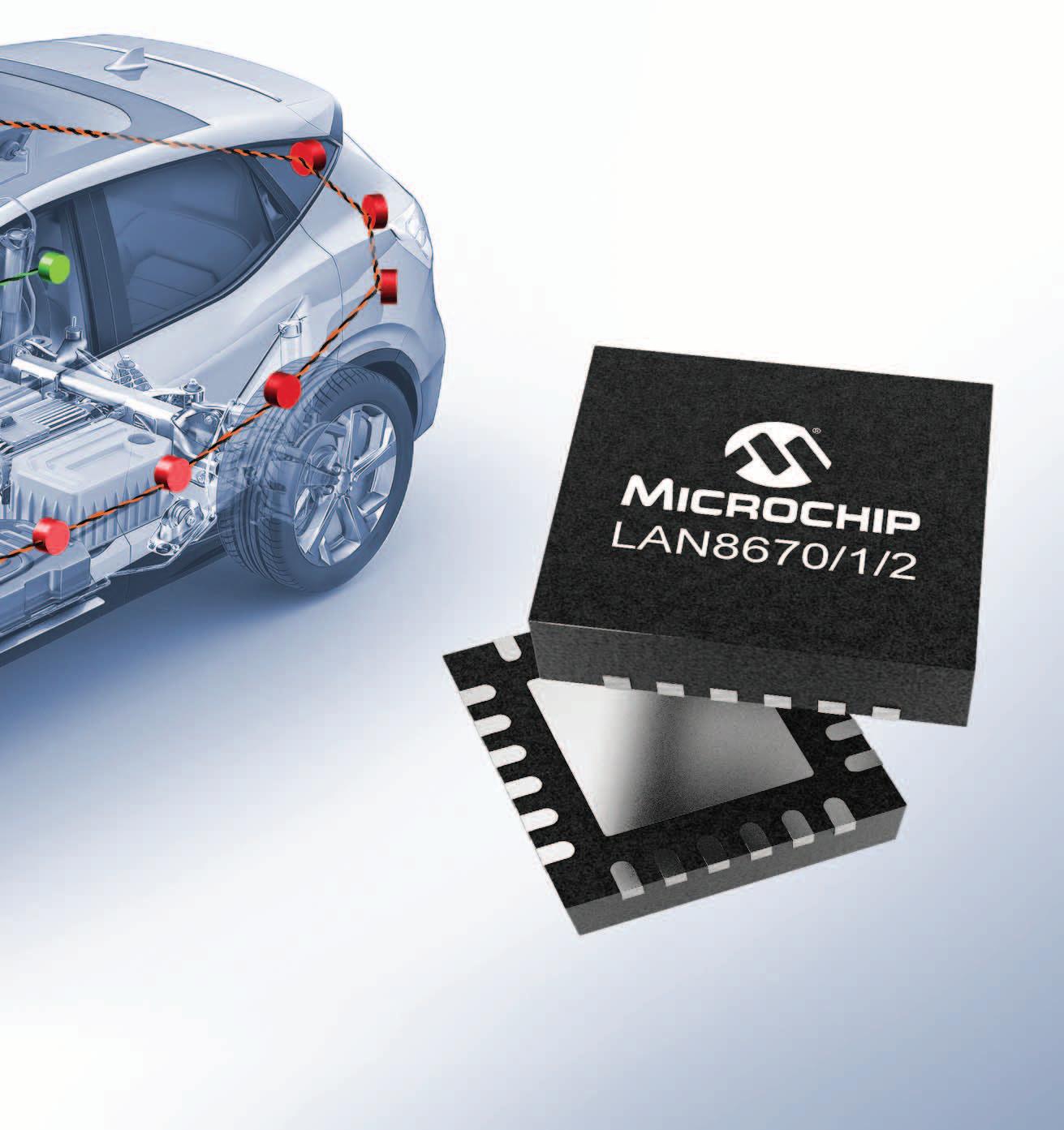

The LAN8670/1/2 10BASE-T1S Ethernet PHYs are supported with the EVB-LAN8670-RMII, EVB-LAN8670-USB and MPLAB® Harmony v3
Pricing and Availability


These devices are available to purchase now. Contact a Microchip sales representative, authorized worldwide distributor or go to Microchip’s Purchasing and Client Services website, www.microchipDIRECT.com
■ Microchip Technology | www.microchip.com

Anritsu Corporation introduces the measurement function (MS9740B-020) for Optical Spectrum Analyzer MS9740B that evaluates a pulsed Laser Diode (LD) chip. New solution reduces the test time for pulsed LD chip, contributing to improved production efficiency of high-power LD chip.


LD chip manufacturers and optical equipment vendors evaluate the optical spectrum of LD chips during manufacturing. Market demand for high-power LD chips is driven by higher communication bit rates and longer LiDAR detection ranges. In addition, new use cases, such as External Laser Small Pluggable (ELSFP) modules for Co-packaged Optics applications, are expected to accelerate demand.
The continuous wave (CW) output from a high-power LD chip suffers power drift and wavelength shift as the chip temperature rises. This is prevented by suppressing the temperature rise by using pulsed LD chips. However, current testing of pulsed LD chips during production takes longer because an external trigger signal is required to synchronize with the pulsed LD chip.
Reduced tact time for pulsed LD chips The new MS97040B020 solution accelerates optical spectrum evaluation by eliminating the need for a trigger signal.
Assured measurement reproducibility for even high-power LD chips. This solution assures measurement reproducibility of ±1.4 dB* for Side Mode Suppression Ratio (SMSR). Low SMSR variation improves the LD chip yield and helps production efficiency.
*) ±1.8 dB with MS9740B-020 installed.
■ ANRITSU | www.anritsu.com
Renesas Electronics announced a new development board for automotive gateway systems. The R-Car S4 Starter Kit is a lowcost, readily available development board for building software using the Renesas R-Car S4 system on chip (SoC). The SoC delivers high computing performance and an array of communication features for both cloud communication and safe vehicle control. The new starter kit is a less-expensive and readilyavailable option compared to the existing R-Car S4 Reference Board, which provides a full-scale development environment including an evaluation board and software. Engineers can take advantage of the new kit to easily start their initial evaluation of car servers, connected gateways, connectivity modules and more, for rapid application development.
The R-Car S4 Starter Kit includes essential R-Car S4 interfaces such as Ethernet TSN switch and CAN FD, as well as memory such as 4GB(Gigabyte) of LPDDR4, 128GB of UFS (Universal Flash Storage), and 64MB(Megabyte) of Quad SPI flash memory. In addition, users can easily expand peripheral functions by using expansion connectors and customize the hardware according to individual needs.
Furthermore, Renesas provides the R-Car S4 Whitebox SDK, an open-source automotive development environment for the RCar S4, which can be combined with the R-Car S4 Starter Kit. The SDK consists of FoC (Free of Charge) software and can be easily used without the need for complicated license agreements. The SDK includes sample software, test programs, and resource monitoring tools for OTA (Over-The-Air software updates), IPS (Intrusion Prevention System), and IDS (Intrusion Detection System) for network security, allowing for various prototyping and evaluation. Users can use the sample software as a base to develop their own applications. This kit shortens development time and reduces energy consumption, thus imposing less impact on the environment.
The R-Car S4 Starter Kit is available from major distributors or via a Renesas local sales representative. For more information, please visit: https://www.renesas.com/R-Car-S4-StarterKit
The R-Car S4 Whitebox SDK will be available by the end of August. Additional information on the R-Car S4 Whitebox SDK is available at: https://www.renesas.com/whitebox-sdk.
■ Renesas Electronics | www.renesas.com

Farnell is stocking the newly introduced BeagleV®-Ahead, the first professional, open-source mass production RISC-V single board computer (SBC) by Beagleboard.org®.
BeagleV®-Ahead is in the same form factor and has the same P8 and P9 cape header pins as BeagleBone® Black, enabling developers to stack their favourite BeagleBone cape on top to expand its capability. Featuring a powerful quad-core RISC-V processor, BeagleV®-Ahead is designed as an affordable RISC-V enabled pocket-size computer for anyone who wants to dive deep into the new RISC-V ISA.
BeagleV®-Ahead is built around T-Head TH1520 RISC-V SoC with a quad-core XuanTie C910 processor clocked at 1.85GHz with a 4 TOPS NPU, support for 64-bit DDR, and audio processing using a single core C906.
Other key features include:
• DA9063 programmable PMIC.

• 4GB Low-Power Double Data Rate (LPDDR4) memory.
• 16GB Embedded Multi-Media Card (eMMC) memory.
• AP6203BM Wi-Fi/Bluetooth connectivity, antennas 2.4GHz and 5GHz.
• Realtek RTL8211F-VD-Cg Gigabit Ethernet with integrated magnetics and RJ-45 connector.
Farnell adds the new
• Micro-USB connectivity with On-the-Go adapter (OTG), Flash support.

• 5V power input.
• HDMI TH1520 video output with mini-HDMI connector.
• Other connectors – microSD, mikroBUS, CSI.
Romain Soreau, Head of Single Board Computing at Farnell, said, “BeagleBoard.org has a strong track record of developing open-source hardware platforms and the launch of BeagleV®Ahead reinforces Farnell’s commitment to fostering innovation and collaboration within the technology community. By making the RISC-V architecture accessible to a broader audience, BeagleV®-Ahead empowers developers to explore new possibilities, accelerate their projects and contribute to the advancement of the RISC-V ecosystem.”
Jason Kridner, Co-Founder of BeagleBoard.org, comments, “We are extremely excited to introduce BeagleV®-Ahead to the world. RISC-V is rapidly gaining momentum as a transformative technology, and we believe that BeagleV®-Ahead will play a crucial role in its widespread adoption. Our goal is to provide a robust, open-source platform that empowers users to unleash their creativity and develop cutting-edge solutions.”
BeagleBoard.org Foundation is a non-profit corporation based in Michigan, USA. Its main goal is to educate and collaborate with people who are interested in open-source software and hardware for embedded computing. The community of BeagleBoard.org provides a platform for owners and developers of open-source software and hardware to share their ideas, knowledge, and experience. They work together to develop physical computing solutions, such as robotics, 3D printers, laser cutters, and industrial and machine controls. The Beagleboard® SBCs are perfect for creating open-source hardware applications, including home and commercial automation systems and AI.
The new BeagleV®-Ahead SBC will be available from Farnell in EMEA, Newark in North America and element14 in APAC.
■ Farnell | https://uk.farnell.com
https://international.electronica-azi.ro


DigiKey announced that it has significantly expanded its portfolio in 2023 by adding over 175,000 new stocking parts year-to-date including nearly 40,000 newly introduced product SKUs across its core business.
“As the industry makes adjustments after three years of a roller coaster ride, DigiKey continues its steadfast commitment to be the industry’s distributor with the largest supplier portfolio and widest product offering,” said Mike Slater, vice president, global business development for DigiKey. “DigiKey continues to add products and the newest technologies in key verticals including automation, power, wireless and automotive in order to maintain our industry leading breadth of product offering. We are delivering the newest and most comprehensive selection of technologies to our customers – engineers, designers and builders – always striving to move their ideas forward.”
Some of the key NPIs now available through DigiKey include: ROHM: The GNP1070TC-Z and GNP1150TCA-Z deliver industry-leading performance in terms of RDS(ON) × Ciss/RDS(ON) × Coss, a figure of merit for GaN HEMTs, translating to higher efficiency in power supply systems. At the same time, a builtin ESD protection element improves electrostatic breakdown resistance up to 3.5kV, leading to higher application reliability. GaN HEMTs’ high-speed switching characteristics also contribute to greater miniaturization of peripheral components.
Knowles: The Knowles V2S200D is designed to selectively pick up the speaker’s voice while suppressing all the other sounds – allowing for a comfortable and frustration-free voice call experience. Its small size, high signal-to-noise ratio and low power offer an ideal solution to customers looking to enhance the user experience of their products.
Renesas Electronics : The RZ/T2L ARM® Cortex®-R52 Microprocessor IC achieves high-speed processing with realtime, high-precision control with EtherCAT to support a multitude of industrial system applications; all while simplifying implementation.

EAO: The EAO Series 09 Universal Switch is ideally suited for use in vehicle interiors. Combining different switches enables a wide range of applications and layouts to be implemented. This design is ideal for safety-relevant applications with a wide range of designs and application-specific configuration options.
Molex: The Molex PowerWize Blind-Mate Interface (BMI) interconnects enable trouble-free mating in drawer-style applications where the connectors are obscured. It is ideal for Telecommunications/Networking, Data Centers and Electric Vehicle (EV) Charging Stations.
For more information about the suppliers in the DigiKey portfolio, please visit the DigiKey website.
■ DigiKey | www.digikey.com

Nexperia, the expert in essential semiconductors, has just introduced the NBM7100 and NBM5100, revolutionary new types of battery life boosting ICs designed to extend the life of a typical non-rechargeable lithium coin cell battery by up to 10x compared to competing solutions while also increasing its peak output current capability by up to 25x compared to what a typical coin cell can deliver without a battery booster. This unrivalled extension in working life will significantly reduce the amount of battery waste in low-power Internet of Things (IoT) and other portable applications while making coin cells a viable power source for applications which could previously only operate from AA- or AAA- batteries. CR2032 and CR2025 Lithium coin cells have higher energy density and longer shelf life. As a result, they are commonly used in low-power applications, including devices with Low Power Wi-Fi, LoRa, Sigfox, Zigbee, LTE-M1, and NB-IoT transceivers. However, these batteries have relatively high internal resistance and chemical reaction rates that reduce their usable capacity when under pulsed-load conditions. To overcome this limitation, the NBM7100 and NBM5100 contain two high-efficiency DC/DC conversion stages and an intelligent learning algorithm. The first conversion stage transfers energy from the battery to a capacitive storage element at a low rate. The second stage utilizes the stored energy to provide a regulated (programmable from 1.8 V to 3.6 V) high pulse (up to 200 mA) current output. The intelligent learning algorithm monitors the energy used during repetitive load pulse cycles and optimizes first stage DC/DC conversion to minimize the residual charge in the storage capacitor. When not performing an energy conversion cycle (standby state), these devices consume less than 50 nA.
Both devices are specified over -40 °C to 85 °C, making them suitable for commercial indoor and industrial outdoor environments. A ‘low battery’ indicator alerts the system when the battery reaches its functional endpoint. In addition, brownout protection inhibits charging of the storage capacitor when the battery is near the end of its life.
To learn more about the NBM5100A/B and NBM7100A/B, visit: https://nexperia.com/battery-management
■ Nexperia | www.nexperia.com
The latest version Universal Debug Engine (UDE) 2023 from PLS Programmierbare Logik & Systeme enables not only efficient but also very convenient debugging and testing of applications developed for Infineon’s TRAVEO™ CYT4DN MCU.
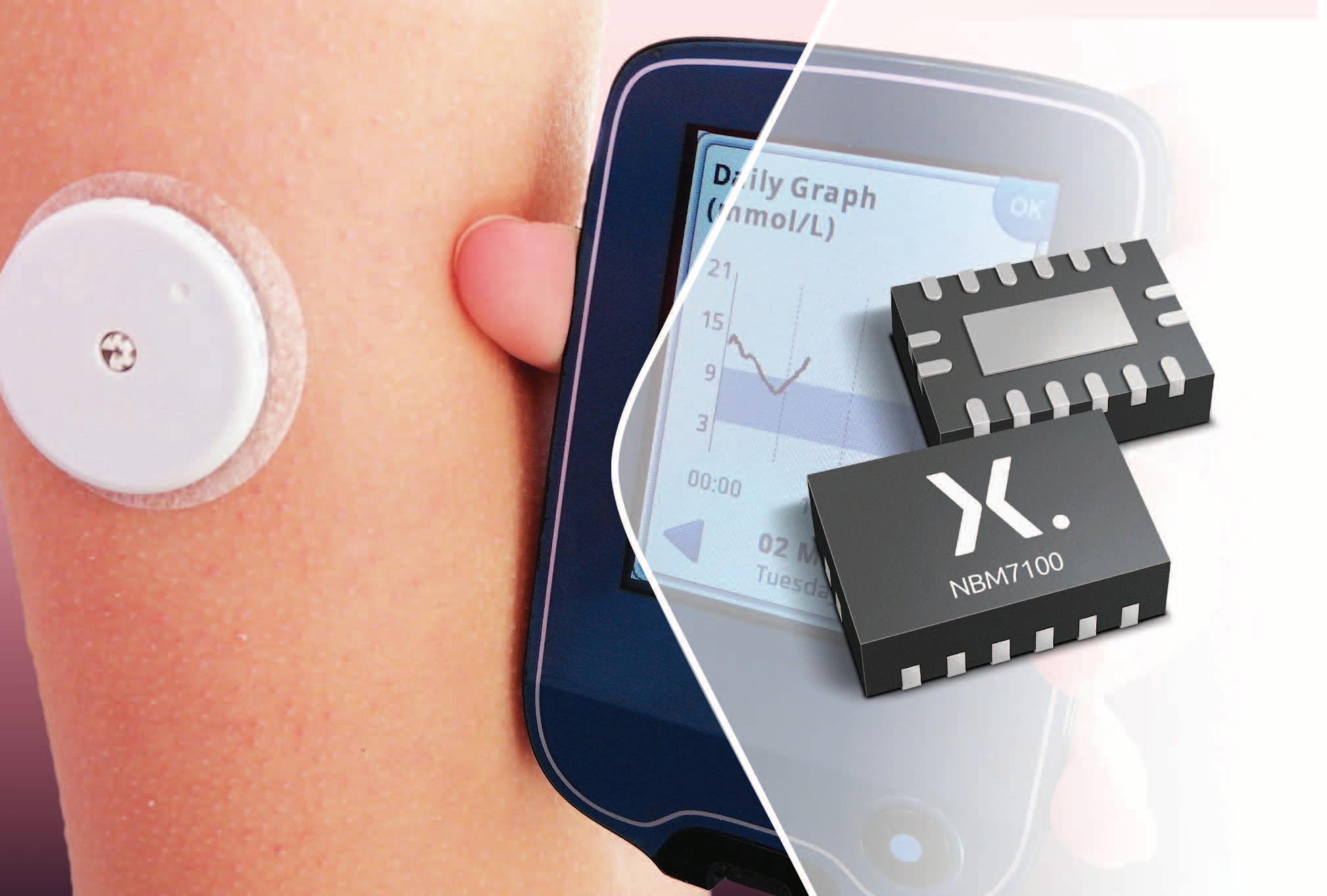
With the latest device CYT4DN of the TRAVEO™ T2G family, Infineon addresses applications in the areas of instrument clusters and head-up displays in vehicles. The device combines two Arm® Cortex® M7 cores clocked at up to 320 MHz with special subsystems for graphics and sound on one chip. An Arm® Cortex® M0+ core is also integrated for security tasks. The memory configuration comprises 6 Mbytes Flash, 640 Kbytes SRAM and 4 Mbytes embedded video RAM (VRAM).
In order to meet the high demands in terms of troubleshooting and software testing, the UDE offers, among other things, true multi-core debugging. All cores are visible in a debugger user interface and can also be controlled from there. It is therefore not necessary to open separate debugger instances for the individual cores. The synchronization of both cores by default ensures that both
Cortex® M7 cores can be stopped simultaneously at a breakpoint and also restarted from there simultaneously. Synchronous single-step operation is thus also possible. If required, this behavior can be modified by the developer so that the debug actions only affect one of the two cores at a time. Multi-core breakpoints enable convenient debugging of shared code. A multi-core breakpoint is always effective, regardless which core is currently executing the code in question. The application is programmed into the flash of the controller via the integrated UDE MemTool.
For developers working with the TRAVEO™ T2G MCUs, the UDE 2023 offers the advantage of a very easy-to-use user interface. It can be easily customized to meet specific requirements and naturally supports multi-screen operation. Freely configurable perspectives make it possible to define multiple views and switch between them to focus on a particular debugging task. Predefined configurations for both the MCUs and the available evaluation boards supported by UDE allow developers to quickly get started with their actual debug or test task without having to worry about detailed settings.
Fast and reliable access to the TRAVEO™ T2G MCUs is provided by the UAD2pro, UAD2next and UAD3+ devices of the Universal Access Device family from PLS. The physical connection to the Arm-specific Serial Wire Debug (SWD) interface is provided by the standard Arm adapter, which can be used universally for all three devices. For demanding environmental conditions, this adapter is also optionally available with additional galvanic isolation.
Support for other members of the TRAVEO™ T2G family of devices is already in the pipeline, so users so users will quickly be able to benefit from a UDE version with device support as they become available from Infineon.
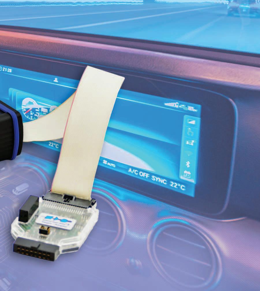
■ PLS Programmierbare Logik & Systeme


www.pls-mc.com
Anritsu Corporation, a global provider of innovative communication test and measurement solutions, is pleased to announce that SPEAG ( www.speag.swiss ) has selected Anritsu’s 5G Base Station Simulator MT8000A for advanced integration in the company’s SAR *1 measurement solution. SPEAG is a leading developer and manufacturer of advanced numerical tools and instrumentation for evaluating electromagnetic near-and far-fields.
The MT8000A is a flexible platform supporting 4G and 5G cellular technology for RF measurements, protocol, and application testing in the FR1 (sub-7.125 GHz), FR2 (mmWave) and LTE. According to SPEAG, integration of the MT8000A in the DASY8-3D V1.4 5G solution significantly simplifies the measurement workflow by enabling automatic 5G call establishment and handovers, enhancing the user experience and ease-of-use.
The MT8000A plays an important role of a “call box” to simulate an appropriate cellular network for a mobile device connection. Once connected, the cellular network then forces the mobile device to transmit at maximum power for subsequent SAR measurement. Creating the conditions for such measurements requires a wide dynamic range for stable connection in the radiated environment, as well as easy parametrization for quick and simple establishment of the connection.
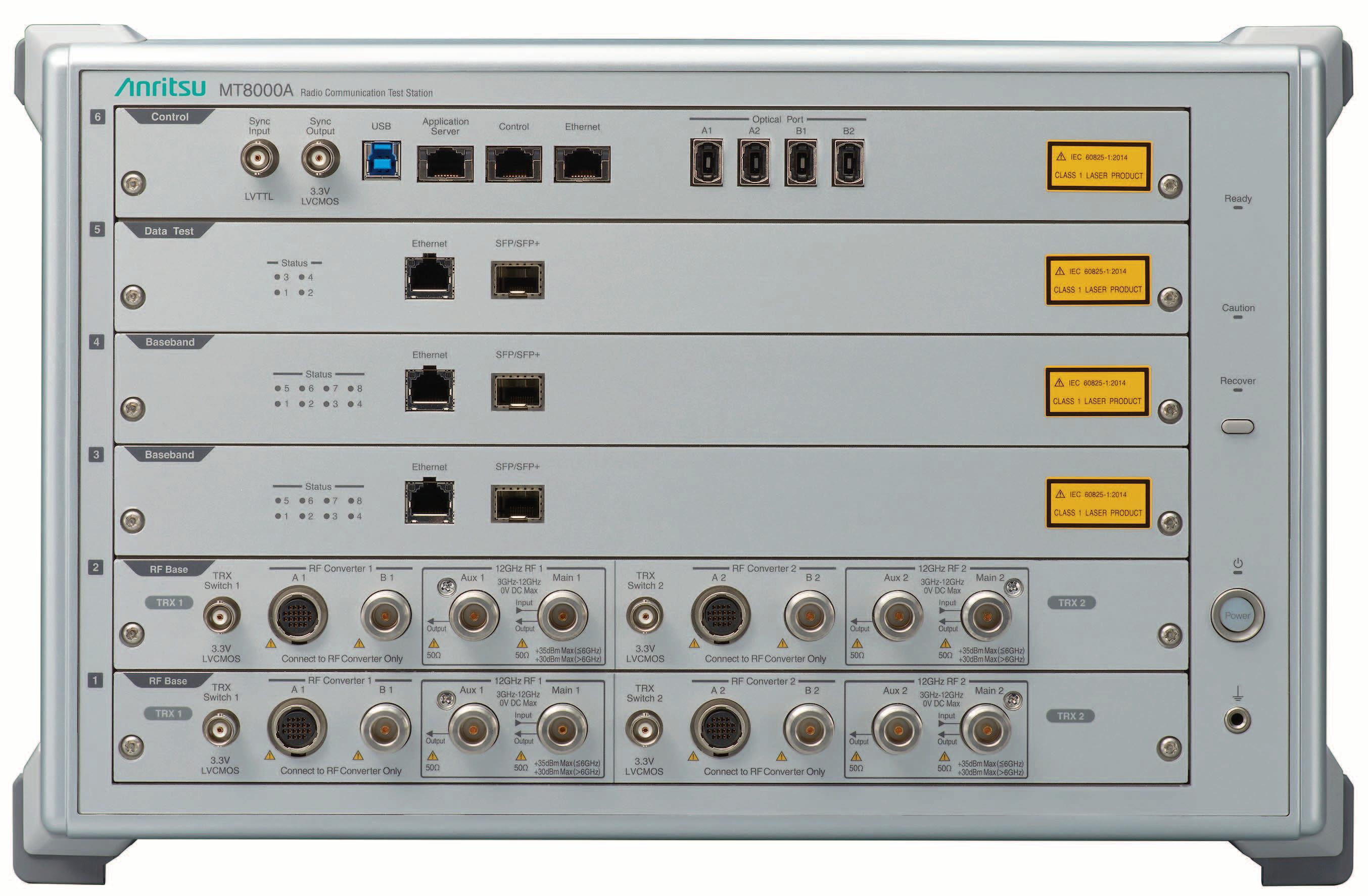
Billions of people use cellular devices daily, so accurate evaluation of generated electromagnetic fields is vital for confidence in the safety and efficacy of the technology. This collaboration with the market leader in SAR measurement, SPEAG, demonstrates Anritsu’s continuing leadership, innovation, and expertise in the telecommunications field.
[ Technical Terms]

*1 SAR: Abbreviation for Specific Absorption Rate; Quantity of average radio frequency energy absorbed by human body.

■ ANRITSU | www.anritsu.com


When carrying out presence control in automated intralogistics and packaging processes, the job of the sensor system is to safely detect the various objects. Handling of the sensor, including mounting, alignment and adjustment, must also be quick and simple, especially as a large number of sensors often need to be installed. This is why a) standardization and b) adaptation of the sensor to the individual needs of the customer are extremely important for the cost-effective commissioning of a system. We have developed an optimized sensor generation for precisely these requirements:
The new 5B series. Highly economical. Perfect handling.
Advantages for you
■ Housing: New, compact housing (dimensions W × H × L: 11 mm × 32.4 mm × 20 mm) – installation-compatible with previous series – ideal for tight installation spaces.
Certified with degree of protection IP 67 and ECOLAB
■ Attachment and mounting: Fast attachment and easy mounting thanks to metal inserts with M3 thread
■ Commissioning: All-around visible 360° indicator LEDs for easy installation and status display. Fast alignment thanks to homogeneous and easily visible light spot

■ Optimal configuration: Easy alignment and adjustment to the application thanks to a user-friendly potentiometer
■ Safe detection of depolarizing objects: Optimized performance for the detection of reflective, shrink-wrapped, and shiny objects
■ Electrical connection: Adaptation to individual customer requirements thanks to different connection options (e.g., cable, M8 connector, pigtail,...)
■ Switching frequency: Improved switching frequency for throughbeam photoelectric sensors with up to 900 Hz for high performance and function reserve


■ Tamper protection: Light/dark switching takes place in a tamperproof manner through polarity reversal of the (cable) wiring
Available operating principles
Retro-reflective photoelectric sensor
Throughbeam photoelectric sensor
Caracteristici
Cost effective mounting
Diffuse sensors

The larger the number of sensors to be mounted on a conveyor line is, the more important the cost effectiveness aspect becomes with respect to the time and cost of mounting and commissioning.
The intelligent and simple fastening concept with two convenient M3 metal threads facilitates fast mounting for the user.
The small and compact housing design also makes installation in small spaces easier.
Depending on your individual preference or local installation situation, various connection types are available, e.g., with M8 connector, cable, or pigtail connector.
Fast and simple commissioning and alignment


360° indicator LEDs ensure easy installation and a clearly discernible status display. Simple alignment of the sensor through the easily visible light spot results in an additional time saving and therefore in a reduction in costs for the user.
Presence control in intralogistics using retro-reflective photoelectric sensors


The new 5B series is also available as a model with potentiometer for better fine adjustment of the sensor. The sensor can thus be quickly and easily adapted to new application conditions. Moreover, the light/dark switching of the switching output can be performed in a tamperproof manner via the wiring.


In conveyor and storage systems, it is often the case that pallets, cardboard boxes and other containers are wrapped in film, which can be challenging for the sensor system. With the new 5B series, we offer optimized models especially for this area of application. These sensors guarantee safe switching even with shrink-wrapped or shiny objects.
Requirement: In a logistics center, various containers and cardboard boxes are to be transported on roller conveyors that are positioned closely to each another. In addition, some cardboard boxes are shrink-wrapped in film. All objects must be reliably detected. During commissioning, the sensor must be fast and simple to install, align, and adjust. The light spot must be easy to see.

Solution: With their compact, space-saving housing, the new 5B series sensors can be mounted directly on roller conveyors that are positioned closely to each other. The sensors are installed and securely mounted using convenient metal inserts with M3 thread. They are aligned quickly and easily using a homogeneous and clearly visible light spot as well as 360° indicator LEDs. Adjustment is user-friendly by means of a potentiometer. Performance optimized for the detection of shrink-wrapped and glossy objects ensures that they can be reliably detected.

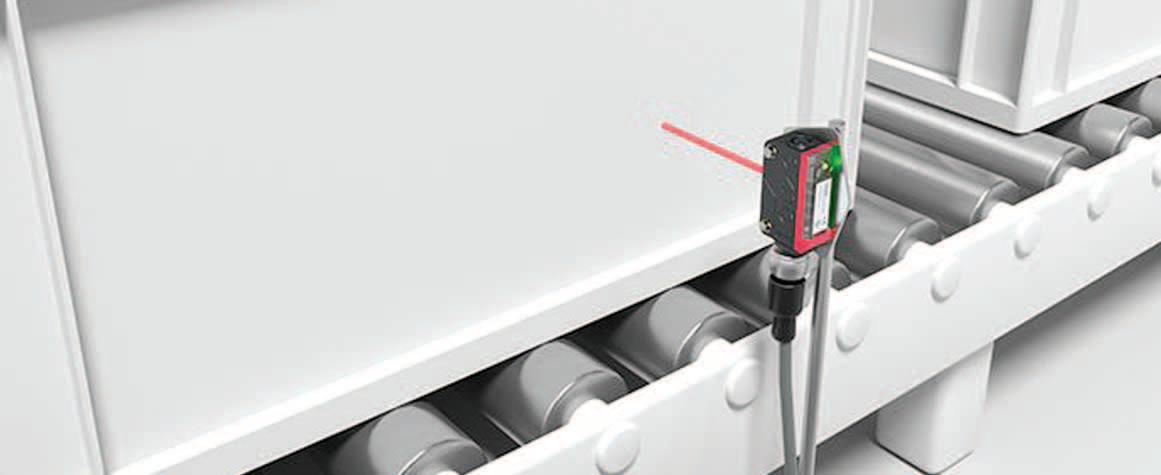
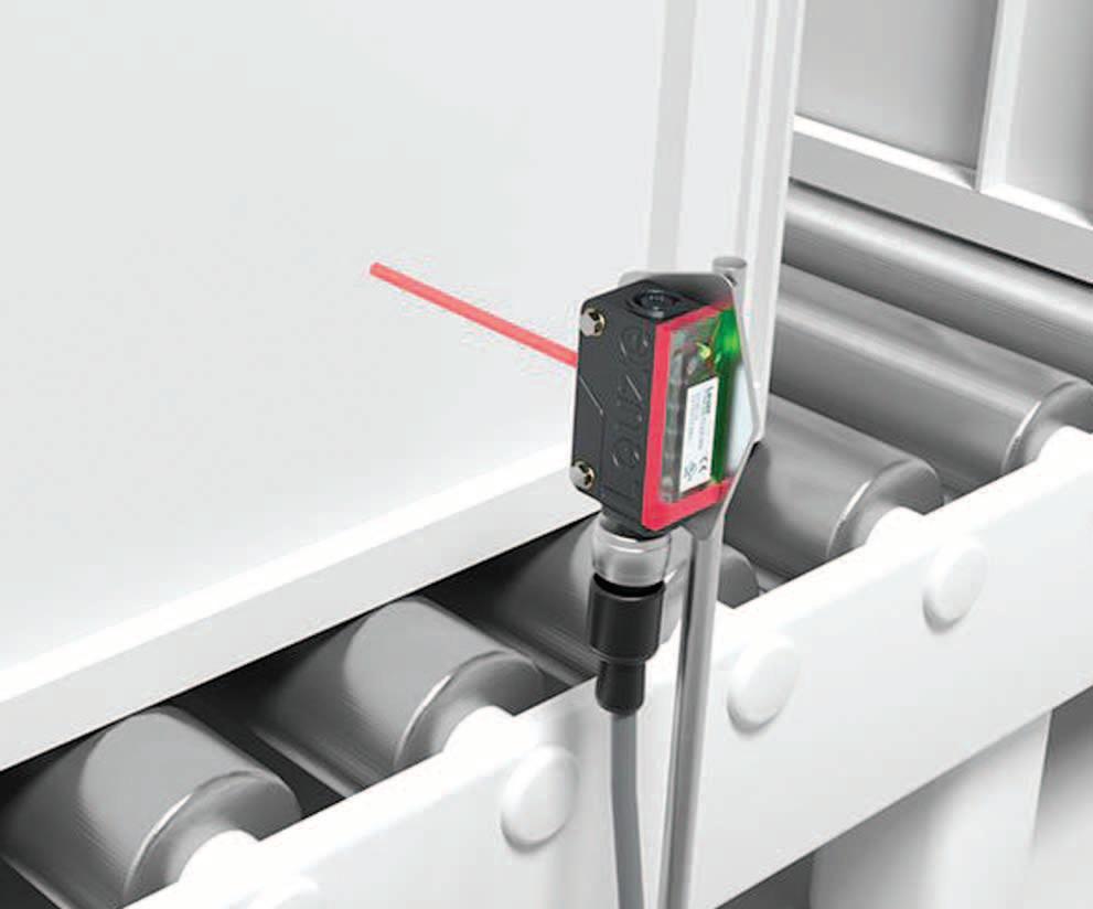
Presence control in packaging systems using throughbeam photoelectric sensors
Requirement: At a food manufacturer's plant, potato chips are packed in primary packaging. The packages are then transported further on a conveyor line where they are to be reliably detected. The light spot must be visible. The sensor state should also be visible from a distance of 2 m.
Solution: The new sensor of the 5B series can also be mounted horizontally on the conveyor line, and the light spot is easy to see. Thanks to the bright 360° indicator LEDs, the sensor state is visible at all times, even at some distance away from the conveyor line. The advantage of the throughbeam photoelectric sensor is the very high function reserve. This ensures reliable detection even in very demanding environmental conditions, and it reduces the risk of system downtimes. Furthermore, the new 5B series has an optimized switching frequency of 900 Hz.

