


1 | 2024 A PAN EUROPEAN MAGAZINE INTERNATIONAL


A corresponding ecosystem of support tools will help simplify motor control system development and accelerate time to market

A corresponding ecosystem of support tools will help simplify motor control system development and accelerate time to market
To implement efficient, real-time embedded motor control systems in space-constrained applications, Microchip Technology has launched a new family of dsPIC® Digital Signal Controller (DSC)-based integrated motor drivers. These devices incorporate a dsPIC33 digital signal controller (DSC), a three-phase MOSFET gate driver and optional LIN or CAN FD transceiver into one package. A significant benefit of this integration is reduction in component count of the motor control system design, smaller printed circuit board (PCB) dimensions and reduced complexity. The devices are supported by development boards, reference designs, application notes and Microchip’s field oriented control (FOC) software development suite, motorBench® Development Suite V2.45.
The integrated motor driver devices can be powered by a single power supply up to 29V (operation) and 40V (transient). An internal 3.3V low dropout (LDO) voltage regulator powers the dsPIC DSC, which eliminates the need for an external LDO to power the device. Operating between 70—100 MHz, the dsPIC DSC-based integrated motor drivers provide high CPU performance and can support efficient deployment of FOC and other advanced motor control algorithms.


An extensive ecosystem of motor control software and hardware development tools help make the design process faster and easier, reducing the customer’s time to market.
The dsPIC33CK Motor Control Starter Kit (MCSK) and the MCLV-48V-300W are two new dsPIC33-based integrated motor driver development boards that provide rapid prototyping solutions with flexible control options. The MCSK includes a dsPIC33CK low-voltage motor control development board, a 24V three-phase BLDC motor, an AC/DC adapter, a USB cable and other accessories. This cost-effective kit supports fast prototyping of motor control applications that operate between 12 and 48 VDC with up to 10 Amps of continuous current.
The MCLV-48V-300W development board enables fast prototyping of three-phase permanent magnet synchronous motors that are rated between 12 and 48VDC and capable of delivering up to 25A RMS continuous current per phase. This inverter board introduces a new modular concept where a separate dual-in-line module (DIM) is inserted into the board to configure it for a particular dsPIC DSC or MCU.
The motorBench Development Suite is a free GUI-based software development tool for FOC that accurately measures critical motor parameters, automatically tunes


feedback control gains and generates source code by utilizing the motor control application framework (MCAF). The latest version, v2.45, includes a powerful new feature called zero-speed/maximum torque (ZS/MT), which enables designers to eliminate Hall or magnetic sensors while maximizing the torque output from the motor, from start-up and at low speeds.
MPLAB® Discover now contains many dsPIC DSC-based MATLAB® Simulink® models supporting various motor control algorithms and development boards. Microchip also provides free device blocks for Simulink that can be used to generate optimized code from models for dsPIC DSCs and other Microchip MCUs.
The growing number of dsPIC DSC-based motor control reference designs now includes an automotive cooling fan, lowvoltage ceiling fan and a drone propeller controller. These reference designs shorten the time to market by providing a production-ready solution for various motor control applications. Typically, the board design files include schematics and a BOM, a board user’s guide and motor control source code that are available for download.
Microchip Technology
www.microchip.com
3 | Microchip Launches New dsPIC® DSC-Based Integrated Motor Drivers that Bring Controllers, Gate Drivers and Communications to a Single Device
6 | Pulsiv to deliver groundbreaking USB-C reference designs & finished modules with more than 95% average efficiency
7 | Infineon unveils high density power modules to enable benchmark performance and TCO for AI data centers
8 | Mouser to Inspire Innovation at Embedded World 2024
9 | Renesas Unveils Powerful Single-Chip RZ/V2H MPU for Next-Gen Robotics with Vision AI and Real-Time Control

10 | PIC & AVR MCUs are Making Edge Node Development Easy
13 | Microchip Expands its mSiC™ Solutions
14 | Power Integrations Launches InnoMux-2
16 | Meeting 5G communication and data center demands with advanced power management technology
22 |

Management
Managing Director - I onela G anea
Editorial Director - Gabriel N eagu
Accounting - I oana P araschiv
Advertisement - Irina G anea
Web design - Eugen Vărzaru

Contributing editors
Cornel Pazara
PhD. Paul S vasta
PhD. N orocel C odreanu
PhD. Marian Blejan
PhD. B ogdan G rămescu
30 | Opening smart locks via a smartphone
32 | New Adapter Board RAB4 from Rutronik System Solutions enables centimeter-precise positioning in real-time
34 | Getting started with Matter
36 | Ecodesign, Reuse, Repair, Prolonging Lifetime and New Technology − Is it the new paradox?
42 | Engaging Attendees and Showcasing Innovations
44 | Vector Offers Dynamic Load Management in Charging Parks
44 | TASKING at embedded world 2024
45 | TriLite announces availability of form factor engineering samples for Trixel® 3 Laser Beam Scanner (LBS), to accelerate development of AR use cases
46 | SemiQon announces successful testing and global shipping of its silicon-based 4-qubit quantum chip and ground-breaking transistors
47 | The goal: Fitting computer- on-modules with everything that application developers need
48 | Navitas GaN and SiC Technologies to Enable Next-Gen AI Power Delivery
48 | Shield enables Click boards to be added to Red Pitaya ‘Swiss Army Penknife’ engineering platform
49 | Nexperia unveils Next Gen Low-Voltage Analog Switches
50 | Mouser Electronics Sponsors 2024 Global Create the Future Design Contest, Now Accepting Entries
50 | Mouser Electronics Celebrates 60th Anniversary
51 | The SMTconnect 2024: Increased synergy effects between electronics production and power electronics
52 | Sensors with convincing cost effectiveness on conveyor lines and in the packaging industry


®
“Electronica Azi” is a registered trademark at OSIM - Romania, Registered position: 124259
ISSN: 1582-3490


Pulsiv to deliver groundbreaking USB-C reference designs & finished modules with more than 95% average efficiency
Pulsiv Limited, the Cambridge (UK) innovator of power electronics technology, is set to release a series of reference designs and assembled modules for USB-C applications that will deliver an average efficiency of more than 95%. This groundbreaking achievement, which minimises energy waste under all operating conditions, has been developed in collaboration with GaN leader, Innoscience and magnetics expert, Frenetic. Designs will be released throughout 2024 to support a new class of sustainable USB-C chargers, adapters, and in-wall sockets. The first 65W solution is expected to be announced towards the end of March 2024.
The front-end of the design utilises Pulsiv OSMIUM technology to efficiently manage the AC to DC conversion process with zero inrush current and no input voltage derating. Using an intelligent active valley fill approach, this patented method also enables the use of smaller system components compared to conventional designs. The DC-DC converter in the 65W variant is based on an industry standard QR flyback. However, when combining a Pulsiv OSMIUM front-end design with optimised magnetics from Frenetic, it is now possible to use an EQ20 core, which provides a 20% reduction in the flyback transformer size.
Frenetic CEO, Chema Molina comments: “By leveraging Pulsiv’s innovative OSMIUM technology, we’ve been able to highly optimise the magnetics to reduce size and drive the efficiency of the flyback transformer to a level we’ve not seen before.
This significant development will enable customers to achieve new levels of performance, size, and cost, and we’re excited to be part of such an innovative solution.”
The use of GaN components from Innoscience has helped to further minimise losses by lowering the RDS(on) and reducing parasitic capacitance, while also optimising the overall BoM cost.
General Manager for Innoscience EMEA, Denis Marcon adds: “We’ve successfully demonstrated that GaN technology is perfectly suited to improving the performance of power electronics designs. Pulsiv OSMIUM technology adds further benefits by significantly improving the overall average efficiency and reducing energy waste. I’m delighted that Pulsiv has selected Innoscience GaN e-mode devices (InnoGaN) for their 65W reference design.”
Pulsiv Chief Product Officer, Dr Tim Moore has been managing the roadmap of USB-C solutions and comments: “We are very excited to be bringing this game-changing technology to the market and deliver our mantra of ‘doing more while using less’. By achieving more than 95% average efficiency, it enables us to provide efficient in-wall USBC solutions that safely manage the critical thermal requirements. This enhances reliability, minimises overall size, and optimises cost to set a world-leading precedent in USBC power supplies.”
Pulsiv continues to demonstrate innovation by delivering cost effective, energy
efficient, and sustainable power electronics designs that benefit billions of devices. To accelerate and simplify the design process, three options will be offered:
Complete reference designs will be made available on the Pulsiv website where engineers can download a document package that includes a datasheet, schematic, bill of materials, and EMC test data.
Fully assembled, ultra-compact, and EMCcompliant finished modules will be produced by Pulsiv to demonstrate a sizeoptimised design and enable rapid prototyping of each reference design. They can also be easily integrated into end products without incurring any further design, development, or manufacturing costs.
Evaluation boards will be developed for customers who wish to test and/or adapt the design for their own requirements and will be stocked by a number of distribution partners. A datasheet with schematic, bill of materials, EMC test data, Gerbers, and PCB layout files will also be available.
To register your interest in this exciting new development and receive full product details upon launch, please click here: Register
https://pulsiv.co.uk
Artificial Intelligence is currently driving an exponential increase in global data generation, and consequently increasing the energy demands of the chips supporting this data growth.
Infineon Technologies AG launched its TDM2254xD series dual-phase power modules that enable best-in-class power density, quality and total cost of ownership (TCO) for AI data centers.
The TDM2254xD series products blend innovation in robust OptiMOS TM MOSFET technology with novel packaging and proprietary magnetic structure to deliver industry-leading electrical and thermal performance with robust mechanical design. This lets data centers operate at higher efficiency to meet the high power demands of AI GPU (Graphic Processor Unit) platforms while also significantly reducing TCO.


Given that AI servers require 3 times more energy than traditional servers, and data centers already consume more than 2 percent of the global energy supply, it is essential to find innovative power solutions and architecture designs that further drive decarbonization. Paving the way for the green AI factory, Infineon’s TDM2254xD dual-phase power modules combine with XDP TM Controller technology to enable efficient voltage regulation for high-performance computing platforms with superior electrical, thermal and mechanical operation.
Infineon introduced the TDM2254xD series at the Applied Power Electronics Conference (APEC). The modules’ unique design allows for efficient heat transfer from the power stage on to the heat sink through novel inductor design that is optimized to transfer current and heat, thereby allowing for a 2 percent higher efficiency than industry average modules at full load.


Improving power efficiency at the core of a GPU yields significant energy savings at scale. This translates into megawatts saved for data centers computing generative AI and in turn leads to reduced CO 2 emissions and millions of dollars in operating cost savings over the system’s lifetime.
“This unique Product-to-System solution combined with our cutting-edge manufacturing lets Infineon deliver solutions with differentiated performance and quality at scale, thereby significantly reducing total cost of ownership for our customers,” said Athar Zaidi, Senior Vice President, Power & Sensor Systems at Infineon Technologies
“We are excited to bring this solution to market; it will accelerate computing performance and will further drive our mission of digitalization and decarbonization.”
Infineon Technologies
www.infineon.com

Mouser Electronics Inc. will inspire innovation at this year’s Embedded World exhibition at the Nürnberg Messe in Nuremberg, Germany. From 9 to 11 April, the embedded electronics community will meet in person to learn more about the latest industry trends and collaboratively generate ideas and concepts for the future.
The Mouser booth will feature a retro 80s gaming kiosk where attendees can go head-to-head in the vintage stacking game, “Pick, Pack, Stack.” The booth will also have the highly popular “spin-to-win” game, giving visitors the chance to win a prize. Additionally, visitors have the chance to win a development kit from one of Mouser’s valued manufacturer partners through its online prize draw. Attendees can also relax and enjoy a freshly brewed cup of coffee, served by a robotic arm. Visitors to the booth will have the chance to talk with the customer service team, who will be ready to answer any queries and guide attendees through mouser.com.
Retro
– “Pick, Pack, Stack”
Step back in time with the retro stacking game – “Pick, Pack, Stack.” Relive the 80’s nostalgia at Mouser’s gaming kiosk as players compete head-to-head, guiding a mBot character to swiftly stack packages without letting them fall. Players will have to keep a watchful eye on the time as this game is a race against the clock. Those who successfully stack the packages in the fastest time will be featured on the arcade-style leaderboard, where
the top 10 players will be determined at the end of the exhibition.
Discover the perfect blend of technological innovation and taste with our cuttingedge autonomous coffee station! With the help of the NXP Semiconductors EdgeReady smart human-machine interface, ordering coffee becomes a breeze. Its advanced machine learning technology enables sophisticated face recognition and keyword spotting capabilities. Just a quick glance and a few friendly words are all it takes, and once the order is received, visitors can continue to be amazed as a sleek robotic arm serves up a freshly brewed, delicious cup of coffee.
Mouser’s customer service team will be at the booth to provide guidance on how to use a wide range of useful online services and tools that can support engineers through the design process. This includes the FORTE Intelligent BOM tool, the Price and Availability Assistant, ECAD design library, and Mouser’s helpful Conversion Calculators. The representatives will also be available to answer any questions regarding orders and delivery times.
Come along to the booth to play Mouser’s ever-popular “spin-to-win” game, where attendees have the opportunity to win a prize from a wide selection of high-quality gadgets and development tools.
Online Prize Draw
Mouser will also be holding an online prize draw for Embedded World 2024, where registrants can enter to win one of the development kits from some of Mouser’s valued manufacturer partners:
• Analog Devices Inc.
ADALM-PLUTO Active Learning Module
• BeagleBoard BeagleV®-Fire Single Board Computer
• Infineon Technologies PSoC™ 62S2 Wi-Fi®Bluetooth® Pioneer Kit
• Nordic Semiconductor Thingy:91™ Multi-Sensor Prototyping Platform
• NXP Semiconductors MCX-N9XX-EVK Evaluation Kit for MCX N94x MCUs
• onsemi NCN26010XMNEVK Industrial Ethernet Evaluation Kit
• ROHM Semiconductor BM2SC123FP2EVK-001 Reference Board
• Silicon Labs SiWx917 Wi-Fi 6 + Bluetooth®LE 5.4 Pro Kit
• STMicroelectronics
STM32H573I-DK Discovery Kit
• Texas Instruments BEAGL-PLAY-SBC BeaglePlay® Single-Board Computer
The Embedded World 2024 online prize draw is open for entries from 4 March 2024 until 3 May 2024. To enter the prize draw and to discover more about what Mouser will be exhibiting at Embedded World, visit https://emea.info.mouser.com/embeddedworld-2024-en (English)
Mouser Electronics www.mouser.com

New Generation AI Accelerator with 10 TOPS/W Power Efficiency Delivers AI Inference Performance of up to 80 TOPS Without Cooling Fan
Renesas Electronics expanded its popular RZ Family of microprocessors (MPUs) with a new device targeting high-performance robotics applications. Offering the highest levels of performance within the family, the RZ/V2H enables both vision AI and real-time control capabilities.
The device comes with a new generation of Renesas proprietary AI accelerator, DRP (Dynamically Reconfigurable Processor)AI3, delivering 10 TOPS/W power efficiency, an impressive 10-fold improvement over previous models. Additionally, pruning technology employed in the DRP-AI3 accelerator significantly improves AI computing efficiency, boosting AI inference performance up to 80 TOPS. This performance boost allows engineers to process vision AI applications directly at edge AI devices without relying on cloud computing platforms.
The details of the new DRP-AI3 acceleration technology were recently presented at the International Solid-State Circuits Conference (ISSCC 2024) in San Francisco.
The RZ/V2H incorporates four Arm® Cortex®-A55 CPU cores with a maximum operating frequency of 1.8 GHz for Linux application processing, two Cortex-R8 cores running at 800 MHz for high-performance real-time processing, and one Cortex-M33 as a sub core.
By integrating these cores into a single chip, the device can effectively manage both vision AI and real-time control tasks, making it ideal for demanding robotics applications of the future. Since the RZ/V2H consumes less power, it eliminates the need for cooling fans and other heat-dissipating components. This means engineers can design systems that are smaller in size, less expensive, and more reliable.
Renesas has applied its proprietary DRP technology to develop the OpenCV Accelerator that speeds up the processing of OpenCV, an open-source industry standard library for computer vision processing. The resulting speed improvement is up to 16 times faster compared to CPU processing. The combination of the DRP-AI3 and the OpenCV Accelerator enhances both AI computing and image processing algorithms, enabling the power-efficient, real-time execution of Visual SLAM used in applications such as robot vacuum cleaners.
To accelerate development, Renesas also released AI Applications, a library of pretrained models for various use cases, and the AI SDK (Software Development Kit) for rapid development of AI applications.
By running these software on the RZ/V2H’s evaluation board, engineers can evaluate AI applications easily and earlier in the design process, even if they do not have extensive knowledge of AI.
Winning Combinations
Renesas has developed the “Visual Detection Single Board Computer” that uses camera images to identify its surroundings, and to determine and control its movements in real-time. This solution combines the RZ/V2H with power management ICs and VersaClock programmable clock generators to support power-efficient industrial robots and machinery. Its efficient design eliminates the requirement for an additional cooling fan, keeping the solution BOM and size down. These Winning Combinations are technically vetted system architectures from mutually compatible devices that work together seamlessly to bring an optimized, low-risk design for faster time to market. Renesas offers more than 400 Winning Combinations with a wide range of products from the Renesas portfolio to enable customers to speed up the design process and bring their products to market more quickly. They can be found at renesas.com/win.
Renesas Electronics
www.renesas.com


When designing robust edge nodes, the embedded system designer often has four considerations at the forefront of their mind: Sensor Interface | Low Power | Physical size | Security. Microchip Technology offers microcontrollers (MCUs) with a wide input voltage range from 1.8 to 5.5V making them invaluable in noisy environments as all signals can be lifted out of the background noise, the ability to source or sink up to 50mA on individual GPIO pins, as well as Industrial (-40°C to 85°C) and Extended (-40°C to 125°C) temperature ranges. Let’s take a closer look at those four considerations in order.
Sensor interfaces come in several common varieties. Commonly, the embedded system designer uses: Analog sensors which output a continuously varying voltage or current, Digital sensors which can use logic levels or data streams such as serial communications, Variable Pulse Width Modulation (PWM) such as throttle position sensors, or Time of Flight sensors used in range sensing. Let’s look at some of those in more detail.
Having the option to choose between Discrete analog vs on-chip integrated analog means the user can select the right analog tool for the job.
By using a larger process technology on our silicon wafers, this means the on-chip analog peripheral is far less susceptible to crosstalk as well as inductive or capacitive noise that increases as manufacturers move to much smaller process technologies.
Microchip’s integrated on-chip analog peripherals are configurable just as the user would configure any other peripheral.
By having peripherals integrated the user can also read them as inputs, for example the user might want to know what the inputs of the comparator are during a particular stage of the program.
Let’s look at some of those analog peripherals starting with op-amps.
• Integrated Op-Amps
Microchip’s integrated op-amps have the associated passive circuitry on-chip as well, such as the internal resistor ladder allowing programmable gain to be set and even changed during runtime. Furthermore, the op-amp configuration can also be changed during runtime meaning the user can switch between inverting, non-inverting, unity gain (voltage follower), and custom discrete configurations during runtime, giving far greater flexibility than using discrete hardware alone, while minimizing the costs associated with discrete hardware. Usually when using discrete hardware, the designer is forced to design their mixed signal application to handle worst-case scenarios and thus some performance sacrifices have to be made. However, using integrated analog peripherals allows the user to build some intelligence into their application, where the embedded system can change op-amp gain, configuration or even cascade them on the fly. This means the user can design their application to optimally handle each different scenario, while taking advantage of the lower power consumption of peripherals when compared to software-centric solutions. It needs to be said that the integrated opamp is not a “magic bullet”, and as such they won’t always be the most suitable for every possible application. For example, if the user finds themselves developing an application where they need superior analog performance, dual-supply configuration, or a specialty variant then they should look at Microchip’s wide range of discrete op-amps. This is a perfect case of choosing the right tool for the job at hand.
• Analog to Digital Converter (ADC) with enhanced features
Microchip’s enhanced ADC peripheral features include hardware functions that traditionally were only available using software-centric drivers, such as accumulation, burst modes, averaging, window comparison, and filtering. As always, these ADC peripherals can use external reference voltages, but they can also use multiple different internal reference voltages along with auto-conversion triggering.
This results in the user having access to the hardware functions that can be used while the CPU is in low-power modes. For example, the user can configure an ADC window comparison that only wakes the CPU when
the input signal is outside that window so that the CPU can process that input signal appropriately. This means the CPU sees far fewer wakes and results in significant power savings, vital in low-power applications. This has the added benefit of reducing system and therefore sensor noise, since digital components such as clocks and PWM can be disabled when not in use.
Usually when an embedded system designer starts developing an application they will attempt, as much as reasonably possible, to coalesce their sensors and devices around a single voltage domain. This is to reduce the added complexity, increased propagation delay, and associated Bill of Materials (BOM) and PCB real estate costs associated with using level shifting circuitry.
• Multi-Voltage I/O
Multi-Voltage I/O (MVIO) allows the user to set up one full I/O port using a second voltage domain between 1.62V and 5.5V. The MVIO peripheral uses only 500nA when in use, making it ideal for low-power applications. All digital behavior in serial protocols (I2C, SPI, USART), PWM, and GPIO all just work on the second voltage domain with input Schmitt Trigger levels being scaled according to the second voltage domain. Additionally, the second voltage rail can be divided down to be available for input to the ADC as a voltage reference.
• Configurable Logic Cell (CLCs)
The user can configure this peripheral as one of several different logic configurations, which dependent on the device includes the following gate configurations: AND, NAND, AND-OR, AND-OR-INVERT, OR-XOR, OR-XNOR. The user can also select from the following latches and flip-flops: S-R latch, J-K Flip-Flop with Reset, Clocked D-latch with Set and Reset, Transparent D latch with Set and Reset.
The user can leverage Microchip’s graphical configuration tools to create custom peripherals more easily for their application requirements.
This could be something as simple as a button debouncer, or more involved such as a hardware driver for WS2812B Individually Addressable RGB LEDs which combines SPI, PWM, and CLC to create a custom driver peripheral.
Traditionally the drivers for these Individually Addressable LEDs, which use a custom communications protocol, are software driven requiring a high-speed system clock, and result in a heavy CPU load. However, by using Core Independent Peripherals (CIPs), the system clock can be reduced, the CPU can spend more time in lower-power modes or even be used to run other tasks concurrently.
Using CIPs also gives the user increased responsiveness compared to using a CPU. This is because peripheral propagation delay tends to typically be in nanoseconds, while interrupt or other latency due to software-centric processing tends to be orders of magnitude greater.
Microchip 8-bit MCUs offer three lowerpower (sleep) modes: Idle, Standby, PowerDown, as well as a Configurable Standby mode where peripherals can be configured as on or off. With all peripherals off and in Power-Down mode the AVR-DB consumes only 700nA, making it ideal for ensuring long battery life in low-power remote sensing edge node applications.
The user can utilize the AVR Event System to pass signals between peripherals without waking the CPU. This results in predictable response times between peripherals, which allows for autonomous peripheral control and interaction, and synchronized timing of peripheral actions. The integrated CIPs are also highly interconnected so that signals can be directly routed between peripherals, making the transfer of data between peripherals much simpler to achieve all while using less power than in a software-centric design.
Microchip’s range of 8-bit PIC and AVR MCUs come in a variety of packages for your design needs, including PDIP, SOIC, SSOP, VQFN, and TQFP. This gives you flexibility when developing your final PCB design. However, be aware that the maximum current rating of the MCU may be limited by the device package power dissipation characteristics.
In recent years there has been a shift away from sensor nodes that do all their processing in the cloud, and towards edge nodes that do most or all of their processing locally before sending the results to the cloud.
This reduces the ongoing costs associated with cloud services by reducing the frequent bidirectional data transfers and computational processing, as well as the increased sensor node power usage by having frequent larger data transfers due to sending raw unprocessed data to the cloud.
Embedded systems designers can pair up a lower power 8-bit MCU that is used for directly interfacing with sensors, with a more powerful 16- or 32-bit device that can be used for the heavier computational load and increased memory requirements associated with more complex and secure communications stacks. By reducing the overall number of data
transfers between the edge node and the cloud service, both the ongoing cloud costs and battery usage can be significantly reduced. Additionally, by leveraging a second, more powerful MCU into their design, engineers can even perform Machine Learning (ML) at the edge, making their system design far more powerful for uncovering patterns in data and yielding useful insights.
Designers can also take advantage of Microchip’s secure elements including the ATEC608B which uses the ECDSA (Elliptic Curve Digital Signature Algorithm) sign-verify authentication for the Internet of Things (IoT) market, making it ideal for robust sensor edge nodes.
By using on-chip integrated peripherals, the user can reduce their PCB design complexity, saving valuable PCB real estate while reducing the total number of components in their BOM.
This is further simplified using graphical software tools MCC/Melody and Harmony to configure the peripherals and system. These can be used to get up and running quickly as they offer a high-level view of the MCU and peripheral features.
This means the user can significantly reduce the amount of time they spend studying their MCUs datasheet.

This is ideal for designers when evaluating new or perhaps unfamiliar peripheral features and generates usable code that can be used in production, or as a handy reference for people who want to develop their own drivers. All MCU and MPU products offered by Microchip can be programmed through MPLABX IDE which runs on Windows, MacOS and Linux using our range of compilers including XC8, XC16 and XC32. The designer can debug their application without leaving the IDE and can use Data Visualizer to connect to the Data Gateway Interface (DGI), serial ports, as well as outputting information in a terminal, or graphically plot data values over time. Data Visualizer can also be used with the Microchip Power Debugger which has two independent measurement channels, can deliver up to 100mA at 1.6V to 5.5V to power the target device, and can measure down to 100nA in the high-resolution channel. This makes the Power Debugger ideal for optimizing low-power applications required to run on a battery for years.
The device datasheet and other useful documentation can be accessed through MPLABX under the Kit Window. Each device datasheet covers a family of devices, allowing the viewer to compare devices within a family to identify the devices that best meet their design requirements. Such requirements include memory, RAM, the type of and number of instances of peripherals, including supported serial protocols and Configurable Logic Cells (CLC). If using a PIC or AVR Curiosity Nano development board, the user can also access the Curiosity Nano Hardware User Guide, GitHub code examples, schematics, and the Altium project files from the Kit Window.
for Programming and Debugging
Microchip offers a variety of hardware tools to evaluate an MCU, such as the Curiosity Nano development boards, which can be used with the Curiosity Nano Base board to allow easy use of any daughter boards using MikroBUS sockets. This makes developing a prototype or proof of concept much easier. Then when the designer starts developing a custom PCB for their application, they can program and debug their application using the PICKit programmer debugger.
By using Microchip’s range of 8-bit PIC and AVR MCUs, embedded system engineers and designers can more easily and quickly develop robust low-power sensor edge nodes than ever before while making fewer compromises. Designers can leverage a powerful suite of Core Independent Peripherals (CIPs), including creating custom peripherals, while using hardware functions that traditionally required power consuming CPU intervention, all while remaining in a lower power (sleep) mode. With PIC and AVR MCUs, Microchip makes development of remote sensing, cloud connected and ML nodes easier than ever!
■ Microchip Technology www.microchip.com

THE HIGHLY INTEGRATED 3.3 KV XIFM PLUG-AND-PLAY DIGITAL GATE DRIVER IS DESIGNED TO WORK OUT-OF-THEBOX WITH HIGH-VOLTAGE SIC-BASED POWER MODULES TO SIMPLIFY AND SPEED SYSTEM INTEGRATION
The electrification of everything is driving the widespread adoption of Silicon Carbide (SiC) technology in medium-to-high-voltage applications like transportation, electric grids and heavyduty vehicles. To help developers implement SiC solutions and fast-track the development process, Microchip Technology introduces the 3.3 kV XIFM plug-and-play mSiC™ gate driver with patented Augmented Switching™ technology, which is designed to work out-of-the-box with preconfigured module settings to significantly reduce design and evaluation time.
To speed time to market, the complex development work of designing, testing and qualifying a gate driver circuit design is already completed with this plug-and-play solution. The XIFM digital gate driver is a compact solution that features digital control, an integrated power supply and a robust fiber-optic interface that improves noise immunity. This gate driver has preconfigured “turn-on/off” gate drive profiles that are tailored to optimize module performance.
It incorporates 10.2 kV primary-to-secondary reinforced isolation with built-in monitoring and protection functions including temperature and DC link monitoring, Undervoltage Lockout (UVLO), Overvoltage Lockout (OVLO), short-circuit/overcurrent protection (DESAT) and Negative Temperature Coefficient (NTC). This gate driver also complies with EN 50155, a key specification for railway applications.
With over 20 years of experience in the development, design, manufacturing and support of SiC devices and power solutions, Microchip helps customers adopt SiC with ease, speed and confidence. Microchip’s mSiC™ products include SiC MOSFETS, diodes and gate drivers with standard, modified and custom options. For more information about Microchip’s SiC portfolio, click here The 3.3 kV XIFM plug-and-play mSiC gate driver is now available for purchase.

■ Microchip Technology | www.microchip.com

New GaN-based ICs combine AC-DC and DC-DC stages into a single power converter; cut power system losses by up to 50 percent
Power Integrations, the leader in highvoltage integrated circuits for energy-efficient power conversion, today announced the InnoMux™-2 family of single-stage, independently regulated multi-output offline power-supply ICs. InnoMux-2 ICs consolidate AC-DC and downstream DCDC conversion stages into a single chip, providing up to three independently regulated outputs for use in white goods, industrial systems, displays and other applications requiring multiple voltages. Elimination of separate DC-DC stages slashes component count, reduces PCB footprint and increases efficiency by as much as 10 percentage points compared to traditional two-stage architectures. Efficiency is aided by the ICs’ 750 V PowiGaN™ gallium-nitride transistors, zero-voltage switching (without an active clamp) and synchronous rectification.
Roland Saint-Pierre, vice president of product development at Power Integrations said: “Most modern electronic systems rely on multiple internal voltages to operate various functions such as computing, communication
and actuation function – typically heat, light, sound or motion of some kind. But losses in each conversion stage are compounded, degrading system performance and generating heat. The InnoMux-2 IC overcomes this challenge by providing up to three independently regulated voltage outputs or two voltage output and a constant current output from a single stage, achieving a compact and efficient power sub-system with low component count.”
InnoMux-2 ICs deliver up to 90 watts of output power with accurate regulation of better than ±3 percent across the full input line, load, temperature and differential current step conditions. Total power system efficiency (AC to regulated low-voltage DC segment) is above 90 percent; the advanced InnoMux-2 controller also manages light-load power delivery, avoiding the need for pre-load resistors and reducing no-load consumption to less than 30 mW. This conserves power for necessary functionality in applications subject to the 300 mW allowance for standby usage under the European energy-using product (EuP) regulations
InnoMux-2 devices leverage Power Integrations’ thermally efficient InSOP™24 and InSOP™28 packages with PCB cooling, so no heatsink is required.
Device options include dual- and threeoutput constant voltage (CV); optionally, one output may be dedicated to constant current (CC) drive, suitable for powering LEDs in displays or for high-speed charging of an internal battery.
Typical applications include TVs, monitors, appliances, networking, home and building automation, LED emergency lighting and industrial power supplies.
Pricing for InnoMux-2 IMX2174F devices starts at $1.11 for 50,000-unit quantities.
For further information, contact a Power Integrations sales representative, or visit power.com.
Power Integrations www.power.com


Devices
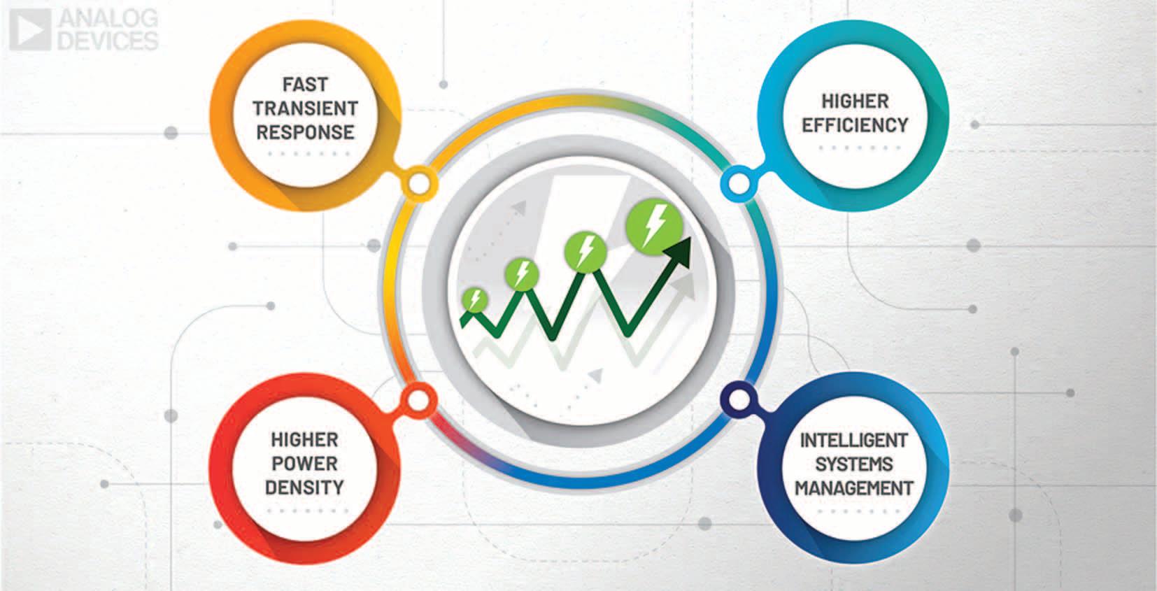
Perched atop a 25 meter mast on the edge of the Mojave Desert, a 5G radio transceiver is exposed to searing heat. The smaller and lighter the radio components and the more efficient the radio’s electronic systems, the less heat they generate and the easier to keep the system cool and functioning. At a data center spread out over 1000 acres, banks of servers are executing millions of searches and high demand workloads to feed an ever-growing information hungry world. The technology demands fast transitioning high currents, with very high power component densities that maximize efficiency to rapidly deliver content.
Across the advancing communications world, the most challenging applications for today’s power electronics face the technical hurdles of size, weight, and power (SWaP). Almost every application seems to be getting smaller and lighter while demanding more power.
The need to optimize SWaP is driving the power electronics industry in many new ways. Power management technology is playing a significant role in the innovation of today’s data center and communication industry.
With sustainability and cost reduction as the goal, technology leadership means higher system efficiency is the target.


With more advanced process technologies being used in communications systems comes lower operational voltages and significantly increased currents, which challenge system efficiency.
Methodologies beyond pure silicon development need to be considered for these next generation systems. This is where ADI is poised to bring advances.
On the wireless side, the emphasis is on maximizing power density and getting to as small a solution as possible to reduce the overall size of 5G applications or provide flexibility to incorporate additional capabilities or functionality. Operating in a smaller space translates to functioning more cost effectively and more efficiently.
Possible options and advances in wireless communications technology are endless. ADI’s deep domain knowledge spans across industries and technologies, providing perspectives and solutions to meet these systems’ growing demands.
Insights include alternative ways of system packaging to impact size, weight, and power that produce a smaller footprint, lower component count, and smaller board area impact.
Reducing the board’s size has the added value of freeing up space to include new technologies or additional functionality such as artificial intelligence (AI) and speech recognition.
Lower noise systems require less shielding; less shielding requires less weight and smaller size.
Electronic technology products require a variety of voltages and currents to operate. Efficient power conversion is key to a well-run system. This means high frequency switching power conversion is needed. A drawback to high frequency switching is the generation of electromagnetic noise interference (EMI) in the RF range. This EMI interference can disrupt the function of highly sensitive devices such as the RF transceiver embedded in a 5G network. ADI’s Silent Switcher® series of power converters operate at high frequency while maximizing efficiency—generating the industry’s lowest electromagnetic interference (EMI). This results in a more robust communication link in cellphone network equipment.
The 5G radio installation is responsible for delivering cell and internet service worldwide, allowing workers, friends, and family to stay in touch. The promise of a globally connected future will undoubtedly have a massive impact on how the world’s population will live, learn, work, and play. Fifth generation wireless technology will require significant advances in power electronics to achieve this goal. And, reliability will be critical, as lives may depend upon it.

Many 5G applications are mission critical and always on. Healthcare workers and emergency responders rely on technology for critical communication and incident alert management.

The need for on-demand data and storage by businesses and consumers is increasing exponentially. To meet these demands, a significant increase in power will be required by data centers. This means efficient power conversion is a critical factor in managing the power demand on our already strained power grid system. Improvements in power management technology are necessary as some data centers consume as much electricity as a small city of 80,000 people.
“ADI brings added value by providing high density, fast response solutions to power the advanced ASICs, CPU, and GPU, which are needed to process all this data,” said Gary Sapia.
Application specific integrated circuits, custom designed for a particular use, are the biggest power consumers.
For the same amount of power, ADI’s solutions help by reducing power conversion losses and lowering heat dissipation.
When you search a picture—say “all dogs with flat noses,” the search engine goes out, crunches the information, and finds it very rapidly from a selection of perhaps two billion choices. This effort requires a special heavy duty processing engine, searching an enormous database that employs artificial intelligence (AI). All these operations require a network of machines to ramp up very rapidly to perform the task, resulting in a rapid spike in power.
Spiking power means spiking current. It’s similar to pushing the pedal of your car’s accelerator—the fuel injector opens up and sprays gas into the engine, taking you across the finish line. When clicking search, you are essentially pushing the accelerator, fueling many servers with power.
McCormick School of Engineering and Applied Science Northwestern University.

These machines need lots of current to execute your request—and they need it now!
To manage current demand in a very short period of time requires special systems that operate with high efficiency and very high bandwidth. ADI’s monolithic integration and proprietary coupled inductor technology allows meeting these stringent requirements while delivering superior efficiency and reducing power consumption.
3 Microseconds (THE TIME IT TAKES FOR ANALOG DEVICES’ POWER MANAGEMENT TECHNOLOGY SOLUTIONS TO SUPPLY HUNDREDS OF AMPS AND LET THE GATEWAYS OPEN. THESE SOLUTIONS PROVIDE A VERY FAST TRANSIENT RESPONSE.)
Whatever your vantage point, wherever you look, the need to reduce size, weight, and power remains a constant for data centers and for all of the communications industry. ADI’s system of circuitry and connectivity products includes integrated circuits (ICs) that manage system information control, data collection and translation, high accuracy data sensors, RF radio solutions, and high efficiency power conversion.
All this packaged as discrete reference designs and in highly integrated application specific module systems solutions known as μModule®.


Data centers, social media companies, connected device manufacturers, cloud service providers, and search engine giants strive to achieve challenging sustainability goals.
The five major U.S. tech companies, affectionally known as FAANG, run hyperscale data centers - super-efficient information factories, each with up to 2.5 million servers.
For almost a decade, they’ve been streamlining computing processes, switching to renewables, and investigating better ways to cool their facilities. These data juggernauts self-imposed a special responsibility to minimize their usage of the planet’s resources.
With the advent of 5G and the requirement for high data rate systems, the processing power of data centers is growing through the roof.
Innovations
Power can make up more than half of a typical data center's costs, with 30% to 40% of that figure attributed to building cooling systems. It makes sound financial and business sense to reduce power consumption when the bill for electric power and cooling the systems continues to be a significant part of the operational expense.
Inefficient power systems produce heat. Therefore, a more efficient power system will require less energy to operate, less space to devote to cooling systems, and less money devoted to fans, heat sinks, and other forms of thermal management. Reducing a data center’s power consumption helps the communications businesses to operate more effectively and sustainably. ADI’s technology can help make FAANG servers more efficient and use less power.
Communications companies powering extremely high current devices no longer rely on reaching power-saving targets with off-the-shelf components. They leverage breakthrough materials and small modules to provide them with new pathways toward smaller and lighter 5G radios. ADI offers tailored solutions to fit customer requirements while considering four vectors of intelligent power management to achieve aggressive power-saving goals.
Size matters equally in a sprawling data center and on the top of a 5G radio mast. Smaller electronics circuits using less metal, plastic, and other resources help technology leaders attain their sustainability targets.
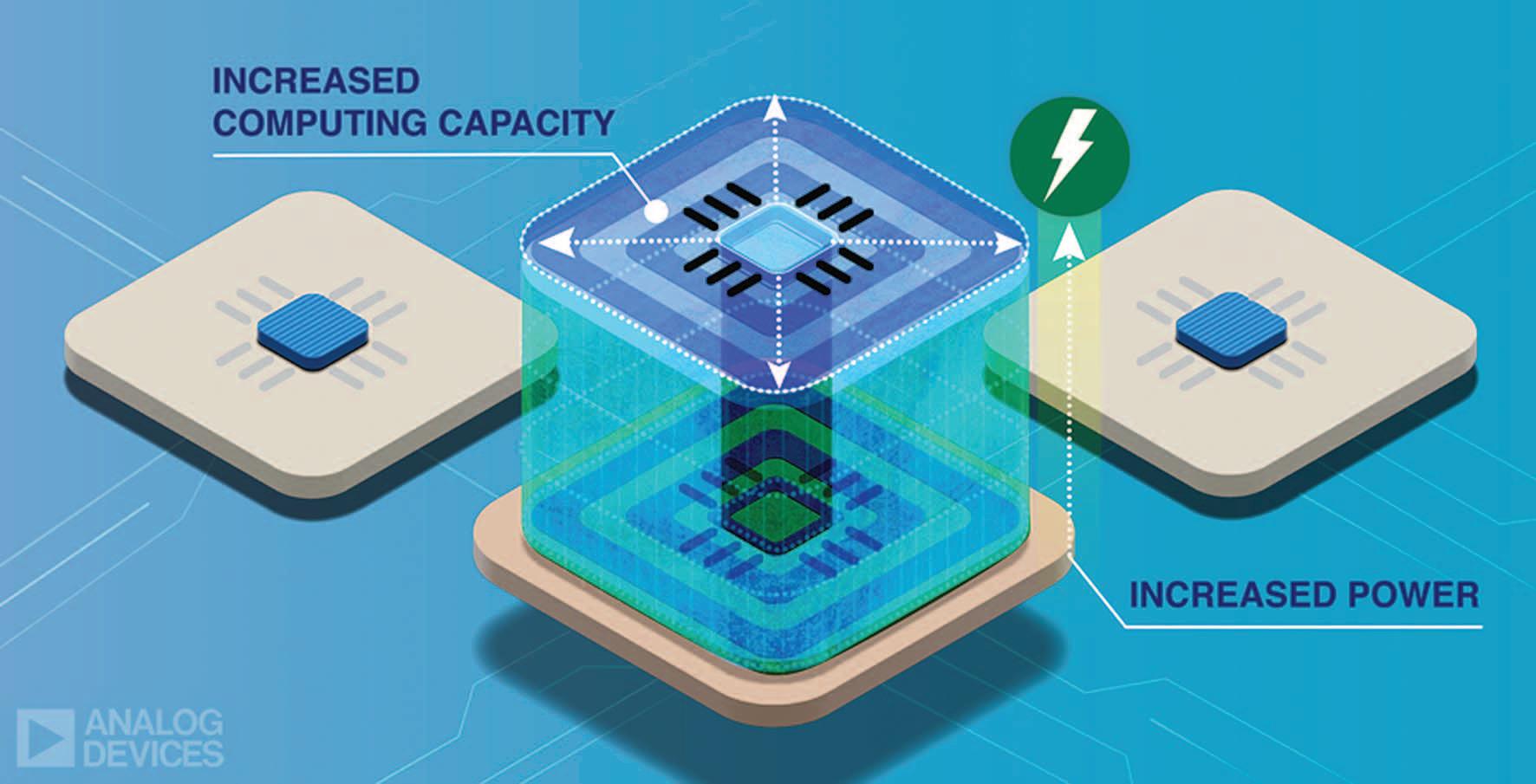
Server system form factors are standard throughout the industry. Increasing ASIC throughput performance requires significant increases in power. Given unchanging size constraints, can engineers increase throughput capacity (the processing of information)?
The answer: ADI engineering makes this possible by providing the highest power density solutions in the industry— adding value with advanced integration and proprietary magnetics, delivering more power at greater efficiency and in less space. Essentially, through ADI innovation, more computing capacity can be packed in the same volume.
A conventional power circuit that down converts an input bus voltage to systemlevel voltages may contain as many as 30 separate components.
By combining these circuit elements into a single μModule device, equipment manufacturers can shrink the footprint of the power circuit, place it closer to the load, simplify the design, and optimize the system performance.
As process technology improves, system voltages get lower and current requirements increase in a nonlinear manner. This dramatic increase in current across the power distribution network (PDN) resistance create losses that significantly impact system power efficiency and power dissipation in the form of heat. As we well know, power loss increases with the square of the current.
Our biggest challenge is to reduce this loss. This is where ADI’s μModule technology meets the challenge head on.
AI or smart power provides the data center operators the ability to monitor power usage and shut down or power up the server racks on-the-fly as needed to conserve energy. Facilities without smart system management may end up with servers being on, unnecessarily, during off peak hours. By using ADI’s smart system management, data center operators can realize up to 25% power savings while reducing electricity bills.
Data centers require enormous amounts of power to operate. Monitoring and controlling this power for failure is critical for safety and reliability. ADI’s intelligent hot swap technology sets the industry standard in providing the needed system monitoring and control that insure safe reliable data center operation.
Hot swap ensures the input current is controlled in a safe manner, preventing component stresses that can cause system failures and component lifetime per-
Improvements in circuit and magnetics design, packaging, and integration are also shrinking the power system in wireless and wired communications equipment. μModule® technology, pioneered by ADI, offers the industry’s highest power density solutions, as multiple power components, making up a complete power solution, are packaged inside a single, surface-mount substrate.
To drive peak operating efficiency, smart system management is required to effectively manage and control the power systems.
5G radio and data center server systems can benefit from new technology today, which enables operators to incrementally improve efficiency and reliability over time by applying insights gained from operational data.
formance degradation. In the event of a fault, hot swap alerts the system and attempts to limit the condition or perform an immediate shutdown to prevent a catastrophic failure, such as a fire.
Hot swap’s intelligent technology manages voltage and current at the rack mounted board level, enabling the safe installation of a backup board (or line card) without the need to power down the entire rack or system.

This allows for the reliable servicing of individual units and minimizes service interruptions - saving time and cost.
ADI’s intelligent hot swap solution is an advanced technology that ensures systems operate in an efficient, safe, secure, and reliable manner, which are critical parameters for any high power data center system.
Mobile phone and internet data services are how most of the world stays connected and informed. The sheer scale of these technologies has a monumental impact, both environmentally and financially. That’s why innovations in power management technology that have the potential to enhance sustainability with increasing efficiency are so valuable.
Creating sustainable solutions that consume less energy is growing in importance across applications. Power semiconductors are central to that objective. But technology is just a starting point.
ADI is committed to making it easier for power electronics system designers to bring safe and reliable data centers and communication innovation to the market as well as reach the goal of a sustainable future that will benefit the planet and its global population.
■ Analog Devices www.analog.com


About the authors
Gary Sapia, received his Bachelor of Science in Engineering from Texas A&M University, with advanced technology courses in power electronics and RF system design. He has over 28 years of experience focused on the design and development of analog systems, including power conversion and high frequency solutions for the communications and GPS markets. Prior to joining Analog Devices, Gary spent 18 years as a field applications engineer at Linear Technology (now part of ADI), focused on Cisco and other prominent Bay Area networking companies.


Andrea Pizzutelli, holds a Ph.D. in information technology and an electrical engineering Laurea degree from Politecnico di Milano in Italy. He has 15 years of experience developing integrated power conversion products and has held various positions focusing on data center, telecommunications, and notebook markets. Andrea has also co-authored multiple scientific papers and holds numerous U.S. patents.
Engage with like-minded members and ADI technology experts in our online community, EngineerZone®. Expand your network, ask your tough design questions, share your expertise, browse our rich knowledge base, or read about new technologies and the engineers behind them in one of our blogs.
Visit https://ez.analog.com


The healthcare industry has been adopting greater use of digital technology over the last couple of decades. The COVID-19 pandemic helped accelerate this evolution. The remote access to healthcare necessitated by the pandemic highlighted several other benefits, such as more efficient healthcare delivery and continuous patient monitoring. Technological advances have spawned the Internet of Medical Things (IoMT), where networks of patients with portable and/or wearable medical devices and sensors, and the corresponding healthcare systems and providers, are connected through the Internet.
Author: Rolf Horn Applications Engineer DigiKeyContinuous blood glucose levels and heart monitors are examples of devices that have gained widespread acceptance. IoMT devices help automate data transfer, thereby reducing human error. Advances in predictive data analytics and artificial intelligence (AI) make IoMT devices even more powerful by enabling data-driven diagnostics with early detection of abnormalities, greater patient self-engagement, and reduced healthcare costs.
Security:
The sensitive nature of the medical information being transferred requires a high level of security. The Advanced Encryption Standard (AES) and Elliptical Curve Cryptography (ECC) can encrypt and decrypt data transfer using secure keys and hence authenticate the data.

Keys based on a true random number generator (TRNG) in the device help in the secure generation of these keys. Spoofing attacks can be minimized with the use of device identification using unique physically unclonable functions (PUF) within the semiconductor device. Secure boot-up hardware protocols, as well as tamperproof mechanisms that prevent access to protected regions of the device memory help enhance device security.
Wearable and portable devices typically run on battery power. Low-power communications protocols such as Bluetooth LE 5.x, power-saving modes when the device is not active, and an efficient architecture that optimizes operational performance versus power consumption are some essential features that can maximize battery life.
Rich feature set in a small size
Small and light devices enable their use in wearable and portable medical applications. New applications such as smart tooth implants require tiny form factors. The System on Chip (SoC) concept provides a high level of multi-functional integration onto a single chip. This can include a peripheral feature set that provides high-speed analog and digital sensing, measurement, data transformation, and communication. Other essential requirements include wireless connectivity, high-speed data processing with large flash and RAM memory, precision low-frequency/low-power clocks and timers, DC/DC voltage regulation, etc.
Silicon Labs EFRBG27 wireless Gecko SoC family for IoMT applications
In March 2023 Silicon Labs aannounced the release of a new family of secure, energy friendly devices that expand their Wireless Gecko portfolio. This includes the BG27 series of Bluetooth LE SoC devices ideally suited for IoMT applications.
A block diagram showing the rich feature set included in the BG27 SoCs is shown in Figure 1. Some details on the key features are listed below:
The 76.8 MHz, 32-bit ARM Cortex® M33 RISC core with DSP instruction and floating-point unit allows for high-performance signal pro cessing capability at 1.50 Dhrystone MIPS/MHz. It includes the ARM TrustZone security technology. The flash memory is 768 kB, while the data memory is 64 kB of RAM. The Linked Direct Memory Access Controller (LDMA) allows the system to perform memory operations independent of the software, hence reducing energy consumption and software workload.
The EFR32BG27 includes an Energy Management Unit (EMU) that manages transitions of the energy modes (EM0 to EM4) of the SoC. With the EMU, applications can dynamically minimize energy consumption during program execution. EM0 mode provides the highest number of features, such as enabling the CPU, radio, and peripherals at the highest clock frequency. Peripherals can be disabled in the low-power active modes EM2, EM3. Voltage scaling is used by the EMU when transitioning between energy modes to optimize energy efficiency by operating at lower voltages when possible. EM4 is an inactive, lowest power state that allows the system to wake up into the EM0 mode.
DC/DC Conversion:
The EFR32BG27 family includes both buck and boost mode onchip converters that can supply the required internal 1.8 V. The boost mode devices, such as the EFR32BG27C230F768IM32-B , have the ability to operate down to 0.8V, allowing single cell alkaline, silver oxide, and other low-voltage battery operation.
The boost converter can be shut down using a dedicated BOOST_EN pin, hence saving system battery power during storage and shipping. In this mode, the maximum current draw is only 20/50nA, depending on the powering of certain pins. In the buck mode devices, such as the EFR32BG27C140F768IM40-B, a maximum 3.8 V can be supplied externally. An on-chip supply monitor signals when the supply is low enough to allow the regulator to be bypassed and extend the range to 1.8 V.
The bypass mode also allows the system to go into the EM4 energy-saving mode. A Coulomb Counter block is integrated into the DC/DC converter. This includes two 32-bit counters that are used to measure the number of charge pulses delivered by the DC/DC converter, enabling accurate battery level tracking to enhance user safety.
Bluetooth 5.x networking:
Bluetooth Low Energy (LE) wireless protocol is supported by this SoC family. The radio receiver uses a low-IF architecture consisting of a low-noise amplifier and an I/Q down conversion. The automatic gain control (AGC) module adjusts the receiver gain to avoid saturation for improved selectivity and blocking performance.
The 2.4 GHz radio is calibrated at production to improve image rejection performance. The family includes a range of transmit powers from 4 dBm to 8 dBm. RF noise mitigation includes operation of the DC/DC converter in soft switching mode at boot, and DC/DC regulating-to-bypass transitions to limit maximum supply slew rate and mitigate inrush current.
The RFSENSE block allows the device to remain in EM2, EM3 or EM4 energy-saving modes and wake up when RF energy above a specified threshold is detected.

DigiKey, a leading global commerce distributor offering the largest selection of technical components and automation products in stock for immediate shipment, has launched season 3 of its “Farm Different” video series, sponsored by Analog Devices, Inc. (ADI) and Amphenol Industrial.
Season 3 features three episodes that provide a look into the future of farming to determine what innovations will power the next generation of global food production. The series explores how robotics and autonomous vehicles are coming to the farm and also dives deeper into the integral data necessary to identify local strategies, maximize yield and help farmers sustainably feed the planet.
“The agricultural community has never backed down when facing sustainability challenges,” said Josh Mickolio, supplier business development manager at DigiKey. “Navigating reduced labor pools, unpredictable weather and rising costs threatens growth in production and the survivability of small and large farming operations alike. This season highlights the fertile future of smart farming, showcasing solutions that leverage the creativity, ingenuity and resilience this industry is known for.”
“With factors such as population growth and climate change, the future will require us to achieve much more with far less, and technology has a key role to play in precision agriculture,” said Tzeno Galchev, marketing director at ADI. “Our technology is helping enable efficiencies across the board. This includes smart edge applications like livestock management and tracking that use our ultralow power technologies, all the way to automating, electrifying, and navigating the machinery that feeds the planet using our inertial measurement units, connectivity, and battery management solutions.”
“In the realm of agriculture innovation, our connectivity solutions are at the heart of empowering farmers to ‘Farm Different,’ ushering in a new era of precision, efficiency and sustainability,” shared Mark Cunningham, general manager at Amphenol Industrial. “At Amphenol, we are committed to enabling the transformation of agriculture, where technology and data converge to cultivate a brighter future for farming.”
To learn more about the video series, sustainable production and how DigiKey is supporting the rapidlychanging agricultural sector, please visit the DigiKey website.
■ DigiKey | www.digikey.com
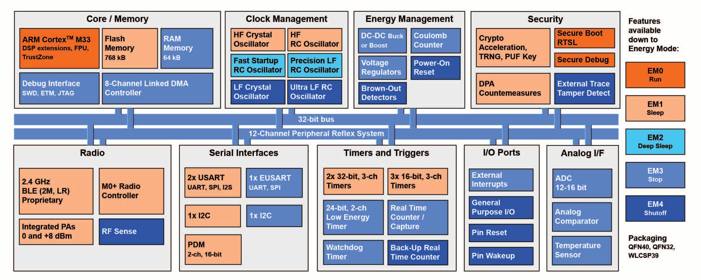
Security: The EFR32BG27 family of SoCs includes a range of security features, as shown in table 1.
The Secure Boot with the Root Of Trust and Secure Loader (RTSL) authenticates trusted firmware that begins from immutable read-only memory (ROM). The cryptographic accelerator supports AES and ECC encryption and decryption. It also includes Differential Power Analysis (DPA) countermeasures to protect keys. The TRNG harvests entropy from a thermal source and includes start-up health tests for this source, as required by the NIST SP800-90B and AIS-31 standards, as well as online health tests as required for NIST SP800-90C. The debug interface, locked when the part is released in the field, has a secure unlock function that allows authenticated access based on public key cryptography.
True random number generator (TRNG)
On the hardware side, an External Tamper Detect (ETAMPDET) module enables detection of external tampering such as unauthorized enclosure opening. It can generate an interrupt to warn the software and allow system-level actions to be taken.
Rich peripheral set: The SoCs include hybrid analog-to-digital converters that combine both SAR and Delta-Sigma techniques. The 12-bit mode can operate at speeds of up to 1 Msps, while the 16-bit converter can operate at up to 76.9 ksps. The analog comparator module can use internal or external references and can also be used to sense the supply voltage. SPI, USART and I2C serial communication modes are all supported. The Real Time Clock and Capture (RTCC) module provides 32-bit timekeeping down to EM3 power modes and can be clocked with the internal low-frequency oscillator.
Secure boot with root of trust and secure loader (RTSL)
Secure debug with lock/unlock
DPA countermeasures
Anti-tamper
Secure attestation
Secure key management
Symmetric encryption
Public key encryption - ECDSA/ECDH/EdDSA
Key derivation
Hashes
External tamper (ETAMPDET)
Using TrustZone
Using TrustZone
• AES 128-bit/192-bit/256-bit
- ECB, CTR, CBC, CFB, CCM, GCM, CBC-MAC, and GMAC
• p192 and p256
• ECJ-PAKE p192 and p256
• SHA-1
• SHA-2/256
The Low Energy Timer (LETIMER) provides 24-bit resolution and can be used for timing and output generation when most of the device is powered down, allowing simple tasks to be performed with minimal power consumption. The Peripheral Reflex System (PRS) is a signal routing network that allows direct communication between the peripheral modules without involving the CPU. This reduces software overhead and current consumption.
Low footprint packages: One of the devices in the EFR32BG27 family is the EFR32BG27C320F768GJ39-B. This device comes in a wafer-level chip scale package (WLCSP) with dimensions of just 2.6 mm x 2.3 mm and can be run in either buck or boost regulator modes. The rest of the family comes in either QFN32 4 mm × 4 mm, or QFN40 5 mm × 5 mm packages in specific regulator modes of either buck or boost.
Conclusion
The EFR32BG27 provides industry-leading energy-efficient processing capability and low-energy Bluetooth connectivity. These small form factor SoCs, that include a variety of security features, are ideally suited for IoMT applications.
■ DigiKey
www.digikey.com

 Author: Prabhath Horagodage Senior Staff Product Management Renesas Electronics

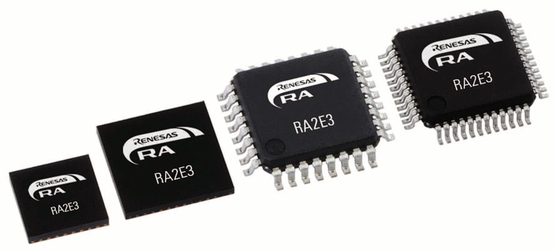
Microcontrollers are used for a variety of purposes. Some applications require high speed, high performance, and continuous full operation, while others require only partial operation at specific cycles. Renesas has been studying these use cases for a number of years and designed the extremely power-efficient RA2E3 to allow designers various means of reducing the MCU power consumption with its power-saving functions. This allows microcontroller-based electronic products to be power efficient and environmentally friendly as expected by end users.
RA2E3 provides four main power-saving functions which can be used either separately or in combination:
1. Three different low-power operating modes
2 Four different power-control modes
3 Switching the clock frequency to an appropriate speed
4. Stopping unnecessary modules for a specific duration
RA2E3 provides the following three different low-power modes:
1. Sleep mode
2 Software Standby mode
3 Snooze mode
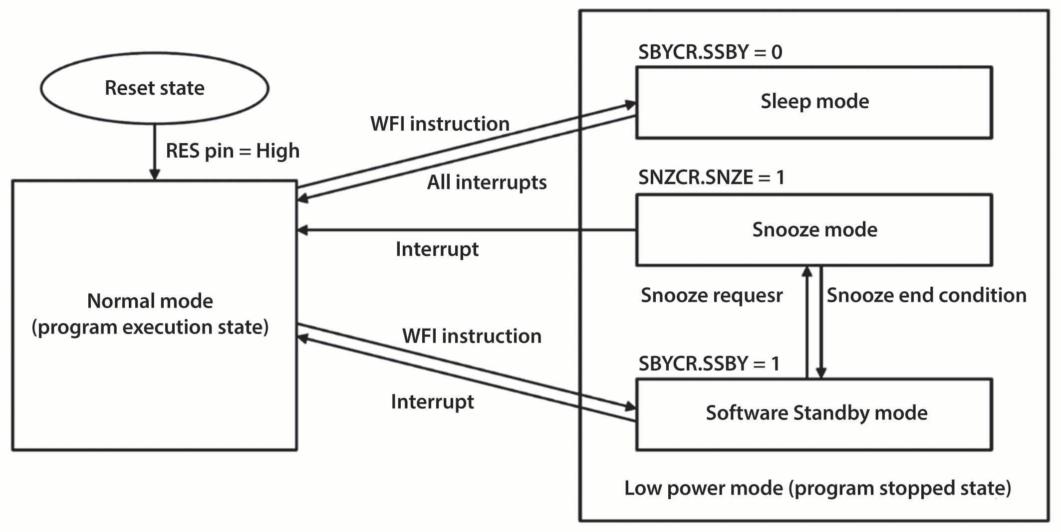
The MCU can be programmed to be transited among these modes automatically when the required conditions are satisfied.
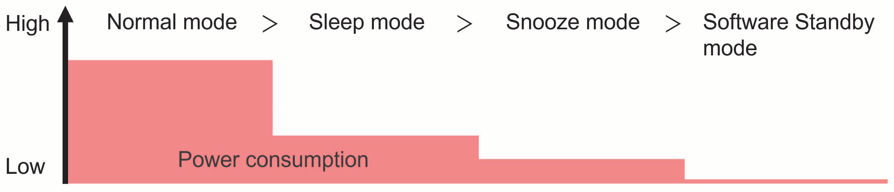
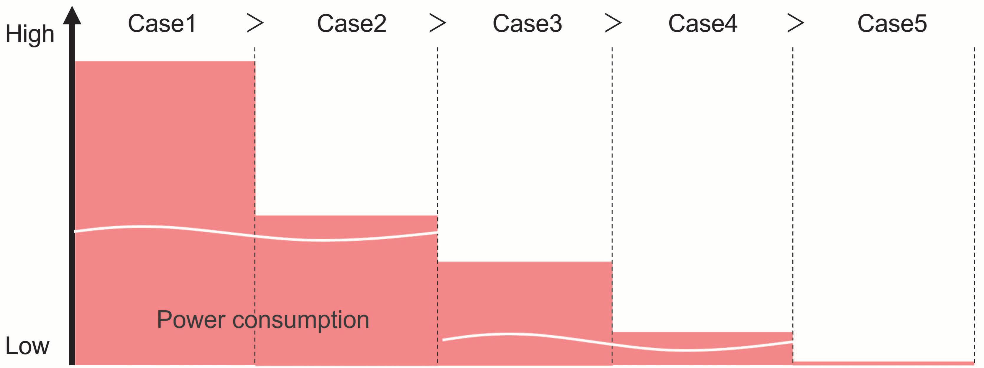
The maximum supply current in the Normal mode with a certain condition (high-speed clocks, all peripheral clocks are enabled, etc.) is 12mA while the typical supply current in the Software Standby mode in a certain condition (all SRAMs are on, all peripheral modules are stopped, etc.) is 0.25μA. Supply currents in Sleep mode and Snooze mode lay between those in Normal and Software Standby modes based on the conditions like number of operating modules, clock frequency, etc. Power consumption in each mode can be roughly compared as in Figure 1. The transition method among low-power modes is depicted in Figure 2.
Sleep mode – in this mode, the CPU stops operating but the contents of its internal registers are retained. Other peripheral functions and oscillators do not stop by default, but the user can set up whether they are to be stopped or not.
For example, if the user needs to execute A/D conversion for a certain period in fast mode but CPU intention is not required in that period, the user can program MCU to enter Sleep mode with a high-speed conversion clock at the start of the A/D conversion and return to Normal mode when the A/D conversion is completed.
In this example, the user saves unnecessary CPU power consumption during that period. Refer to the RA2E3 hardware manual for more details about entering into, operating in, and canceling the Sleep mode.
Software Standby mode – in this mode, the CPU, most of the peripheral functions, and oscillators stop. However, the contents of the CPU internal registers and SRAM data, the states of on-chip peripheral functions, and the I/O ports are retained.
Software Standby mode allows a significant reduction in power consumption because most of the oscillators have stopped. For example, if an MCU needs to wait for an external input like IRQ interrupt to initiate a specific operation and no other operation is required during that waiting period, the user can program the MCU to stay in Software Standby mode until the input is received, saving most of the unnecessary power consumption. Once the input is received, the target operation can be executed in Software Standby mode or after transit to either Snooze or Normal mode as required. It is possible to return to Software Standby mode again after the completion of the target operation and wait for the next input.
Direct transition to the Normal mode form Snooze mode can be made, however.
Let’s look at an example using the UART in Snooze mode. Before starting the UART communication, the MCU can stay in Software Standby mode saving power. When it starts to receive the UART data, the MCU can transit to Snooze mode and continue receiving data without waking up the CPU, unnecessary peripheral functions, and oscillators. Once the data receiving is completed, the MCU can return to Software Standby mode again and wait for the next UART data. Refer to the RA2E3 hardware manual for more details about entering into, operating in, ending and canceling the Snooze mode.
Refer to the RA2E3 hardware manual for more details about entering into, operating in, and canceling the Software Standby mode.
Snooze mode – in this mode, the CPU stops operating but the contents of its internal registers are retained. Operation of most peripheral functions and oscillators are selectable. As depicted in Figure 2, direct transition to Snooze mode from Normal mode or Sleep mode is not allowed. Transition to Snooze mode should be made through the Software Standby mode.
There are four power-control modes which are defined mainly based on the maximum operating frequency and the operating voltage range. The current consumption of memory (Flash/RAM) is reduced by controlling the memory reading speed according to the power-control mode. Users can select the power-control mode as it meets the appropriate operating frequency and power consumption. Power-control modes can be used in Normal, Sleep, and Snooze modes. Power consumption in each mode is shown in Figure 3.
High-speed mode – in this mode, the maximum operating frequency and voltage range during flash reading are 48MHz and 1.8V to 5.5V respectively. The maximum supply current in this mode with a certain condition (operating in Normal mode, all peripheral clocks are disabled, CoreMark code executing from flash) is 4.80mA.
Middle-speed mode – in this mode, the maximum operating frequency and voltage range during flash reading are 24MHz and 1.8V to 5.5V respectively. However, the maximum operating frequency is 4MHz when the operating voltage is 1.6V to 1.8V. The typical supply current in this mode with a certain condition (operating in Normal mode, all peripheral clocks are disabled, CoreMark code executing from flash) is 2.60mA.
Low-speed mode – in this mode, the maximum operating frequency and voltage range during flash reading are 2MHz and 1.6V to 5.5V respectively. The typical supply current in this mode with a certain condition (operating in Normal mode, all peripheral clocks are disabled, CoreMark code executing from flash) is 0.30mA.
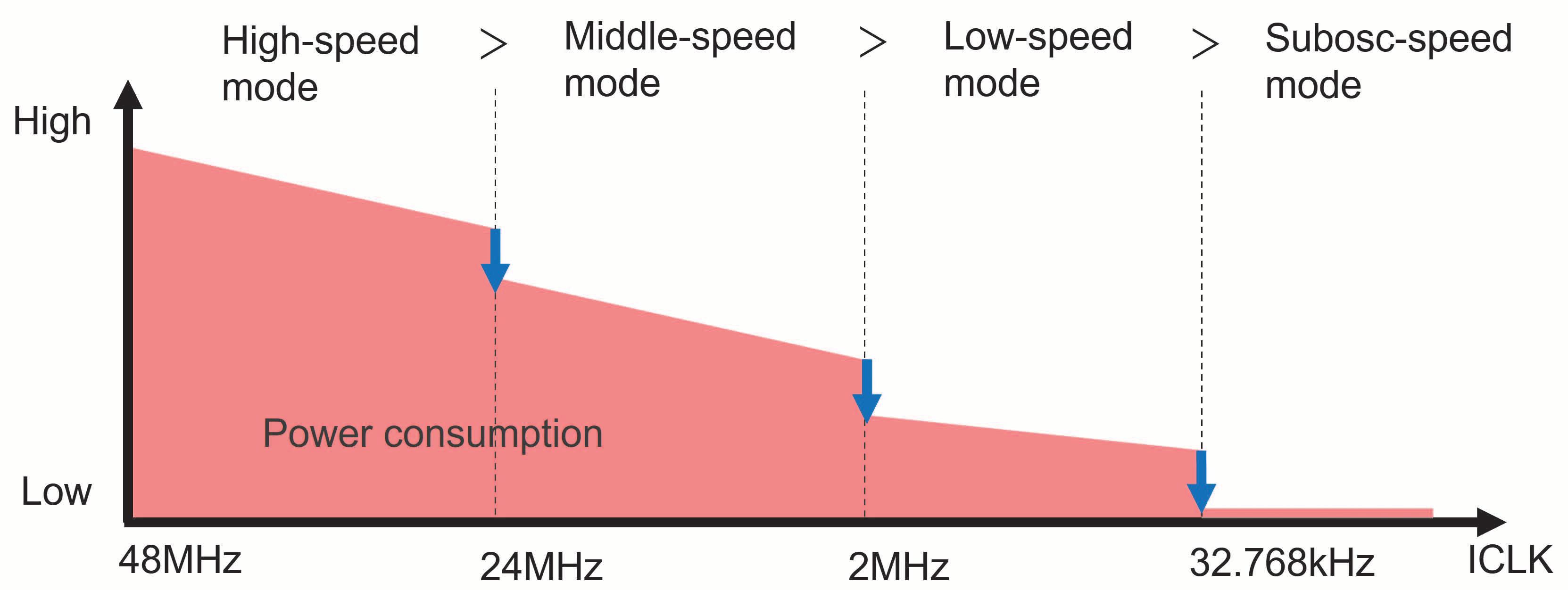
Subosc-speed mode – in this mode, the maximum operating frequency and voltage range during flash reading are 37.6832kHz and 1.6V to 5.5V respectively. The typical supply current in this mode with a certain condition (operating in Normal mode, all peripheral clocks are enabled, etc.) is about 5μA.
The frequency division ratio can be selected for the system clock (ICLK). When a high-speed clock is not required, the user can switch to the appropriate lower-speed clock and save power consumption. Clock division ratios are 1, 2, 4, 8, 16, 32, and 64.
The lower the frequency, the lower the current consumption. But in terms of power performance (mA/MHz), 48MHz is the most efficient (100μA/MHz = 4.8mA/48MHz).
In general, for applications that require higher calculation processing and CPU performance, lower power consumption can be achieved by setting the frequency higher and shortening the CPU processing time in Normal mode.
On the other hand, for applications like control systems, current consumption can be reduced by setting the frequency to a lower value in Normal mode.
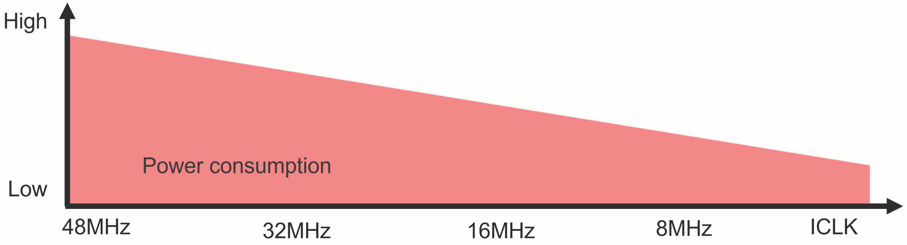
For example, the typical supply currents when the ICLK is 48MHz, 32MHz, 16MHz, and 8MHz are 4.80mA, 3.45mA, 2.05mA, and 1.40mA respectively under the condition of following power-saving functions. Low-power mode: Normal mode, Power-control mode: High-speed mode, Module stopping : all the peripheral clocks are disabled.
The clock division ratio 1, 2, 4, 8, 16, 32, and 64 can be selected for the peripheral clocks (PCLKB, PCLKD) too.
Power consumption can be saved by stopping non-operating modules or their clocks with the following register settings:
• Operation of DTC, I2C, SPI, SCI, CAC, CRC, DOC, ELC, AGT, GPT32n, GPT16n, POEG, ADC120 modules can be stopped by the setting of the MSTPCRn (n: A, B, C, D) registers
• Register R/W clock for RTC, WDT, IWDT can be stopped by the setting of the LSMRWDIS register
• Operating clock for MPU, Debugging, BPF can be stopped by the setting of the LPOPT register
• 8KB out of 16KB of SRAM can be powered off in Software Standby mode by the settings of PSMCR register
More power savings can be achieved using the power-saving functions in combination. The table details five cases that are just a few examples among the many possible combinations.
For additional information on the ultra-low power RA2E3 MCUs: www.renesas.com/ra2e3
■ Renesas Electronics
www.renesas.com

 Author: André Becker, Field Application Engineer Semiconductor & Wireless Central Europe Rutronik

An electromechanical lock is called “smart” if it can be opened and closed by wireless communication with an electronic key. Mobile devices, such as smartphones, wearables, and other tokens, assume the role of a traditional key. Communication between the key and the lock is usually via Bluetooth, Wi-Fi, or near-field communication (NFC).
These smart locks allow secure and convenient access control by making physical keys outdated. New keys can also be conveniently managed, which is a big advantage in buildings with multiple locks. That is why smart locks are a rapidly growing segment in the IoT sector.
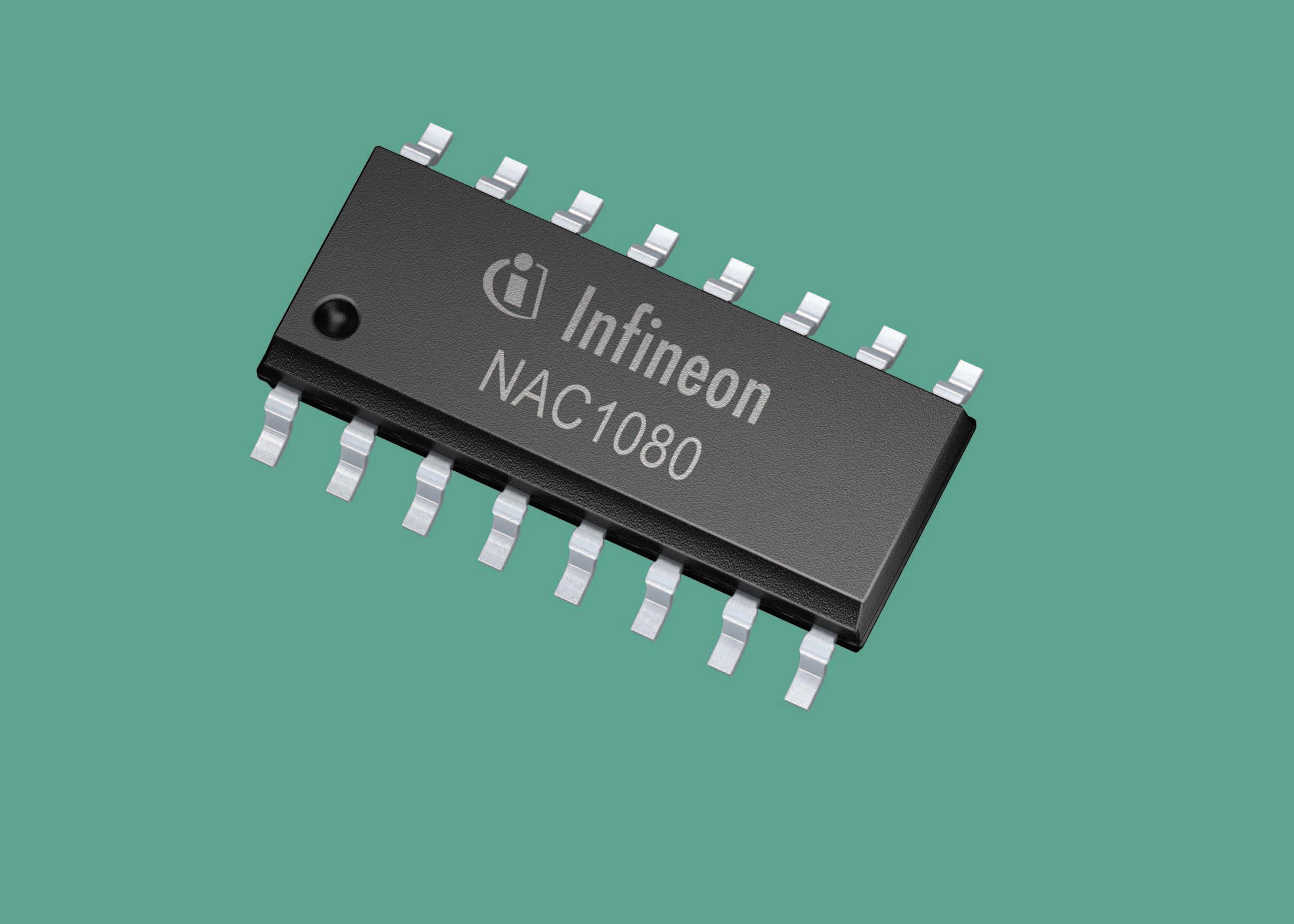
Smart locking systems are increasingly replacing traditional locks. For these innovative lock models, Infineon’s NAC1080 fits like a key in a lock, as it combines NFC, motor control, and energy harvesting in one chip. This eliminates the need for an additional power source, which obviously reduces costs.
For example, the market research and consulting firm Grand View Research put the global market at US$ 1.95 billion in 2022. It is expected to grow at a compound annual growth rate (CAGR) of 19.6 percent between 2023 and 2030, driven by a growing adoption of advanced communication technologies, convenience, and increased interest in advanced security systems.
Smart locks essentially consist of a traditional mechanical lock and an electronic control unit.
A microcontroller authenticates the user through a digital key exchange (e.g. via NFC) and passes the subsequently sent control commands to the motor drivers to lock or unlock a lock. Previous applications with an electrical power source operate as active participants in NFC communication. As a result, the motors that control the mechanical part of the lock are also supplied with electricity by this power source.
A smart lock based on Infineon’s NAC1080 NFC controller, which acts as a passive NFC participant, uses the voltage

induced by the active NFC participant for communication and to power the application, including the motor. With this energy (which is temporarily stored in the capacitor) and an integrated H-bridge driver, the NAC1080 can drive small motors in the milliwatt range (up to 250 mA load current).
The combination of passive NFC operation and a double-layer capacitor eliminates the need for an additional power source, such as batteries or accumulators, thereby reducing costs. The actual charging process takes only a few seconds and does not require an additional battery management system.
When the NAC1080 is accessed by the user, the AES128 symmetric encryption method with a random number generator provides the required security. A universal asynchronous receiver/transmitter (UART) or serial peripheral interface (SPI) can be used to read documented log files.
Microcontroller combines NFC interface and motor driver
This makes it possible to assign the operation of the hardware to the users at any time. The NAC1080 is based on a programmable 32-bit Arm Cortex M0 core operating at a CPU frequency of 28 MHz. It is available in DSO-16 (4 mm × 10 mm) and VQFN32 (5 mm × 5 mm) packages.
If the NAC1080 is integrated into larger locking systems and used as a passive component, it can continue to be used despite a power failure, empty batteries in the smart lock, or loss of keys.
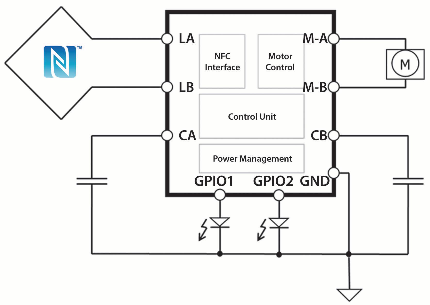
Using an SPI interface, the NAC1080 can communicate with external devices.
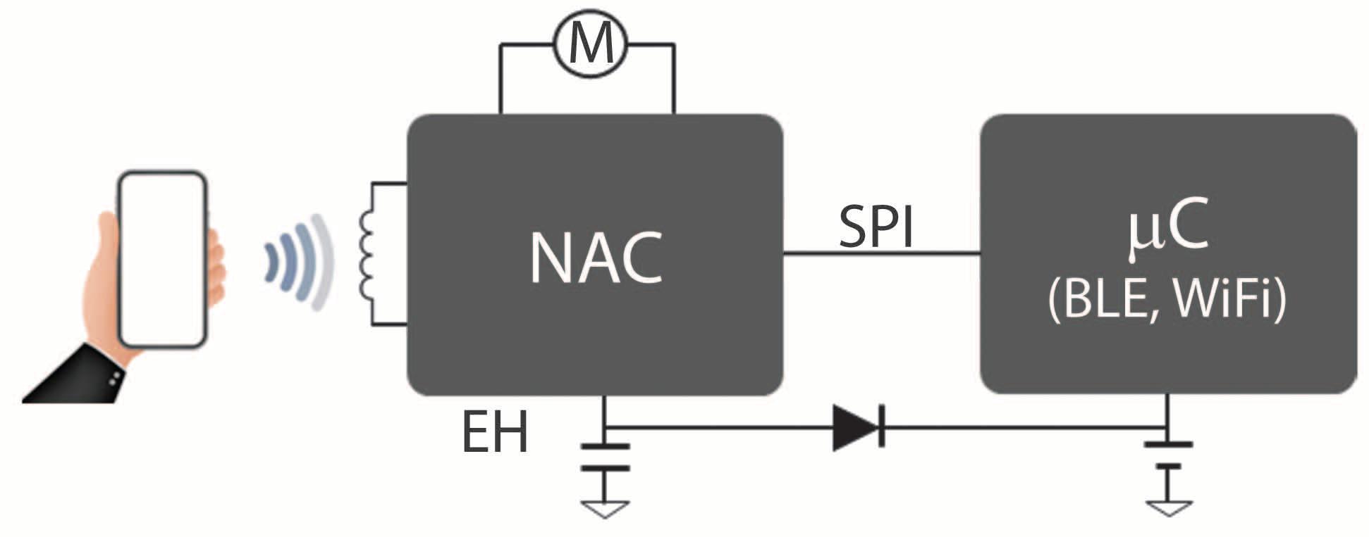
An evaluation kit, included software libraries, and a cell phone app enable developers to carry out quick commissioning.
With this single-chip solution, compact locks that require only a low level of torque can be developed easily and cost effectively. Examples include office cabinets, bicycle locks, and mailboxes. They can be opened within a few seconds. Depending on the components and smartphone used, opening time can vary. In addition, other applications are also possible, such as sensors that are not directly accessible for tire pressure testing.
In this scenario, the IC also powers the door lock directly via the NFC interface.
■ Rutronik www.rutronik.com
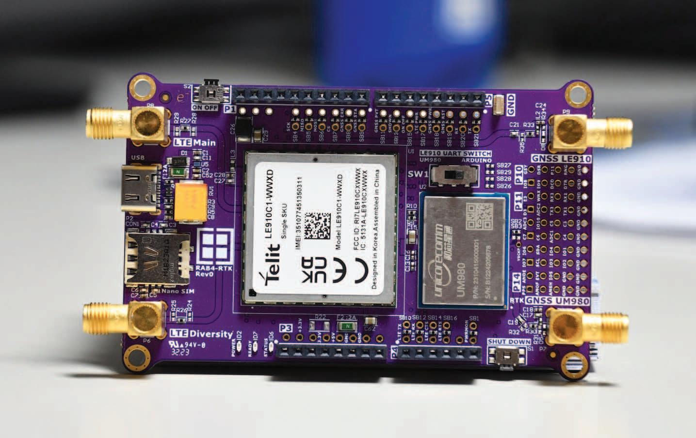
Precise positioning has become increasingly important in many areas and applications. Real-Time Kinematic (RTK) offers significantly greater accuracy than conventional multi-GNSS systems and continues to grow in cost-effectiveness. Together with the Rutronik Wireless Competence Center, the experts from Rutronik System Solutions have developed the Adapter Board RAB4, which facilitates testing the performance of RTK without designing any hardware. By accelerating the pre-development phase and reducing costs, the RAB4 helps to bring applications to market faster.
Autonomous vehicles, drones, and also agricultural machines rely on accurate positioning in real-time. RTK increases the
precision of satellite system positions using a base station that sends correction data to a moving receiver. That allows an accuracy of one to two centimeters, even with fast-moving objects.
The RAB4 features high-performance components, all available on the Rutronik Linecard. The high-precision UM980 RTK positioning module from Unicore Communications uses the latest generation of the NebulasIV GNSS SoC, offers a high positioning rate, and supports all available GNSS frequencies. It is ideal for navigation and positioning applications.
For absolute positioning, a 4G LTE module with an integrated standard multi-GNSS receiver from Telit Cinterion’s LE910 series is integrated on the Adapter Board. Another advantage is that the integration of a GNSS and RTK receiver makes it possible to compare the outputs directly with each other without having to use several development kits from different suppliers.
The RAB4 also includes a 100 MB prepaid SIM card. Thanks to this combination, NTRIP correction data can be downloaded from the Internet. It is not necessary to operate an own reference station.
The modular concept enables a wide range of development projects
Thanks to the Arduino interface, the RAB4 is easy to combine with other boards like the RDK3 from Rutronik System Solutions, a Base Board that allows wireless connections to be realized using Bluetooth® Low Energy. The application example from Rutronik System Solutions demonstrates how the connection works.
Using this example, a rover was developed in-house that can be controlled with centimeter precision via an app. It will celebrate its premiere at the Rutronik booth at embedded world 2024 in Nuremberg.
Further information about the Adapter Board RAB4 and the application example from Rutronik System Solutions is available at www.rutronik.com.
Rutronik www.rutronik.com
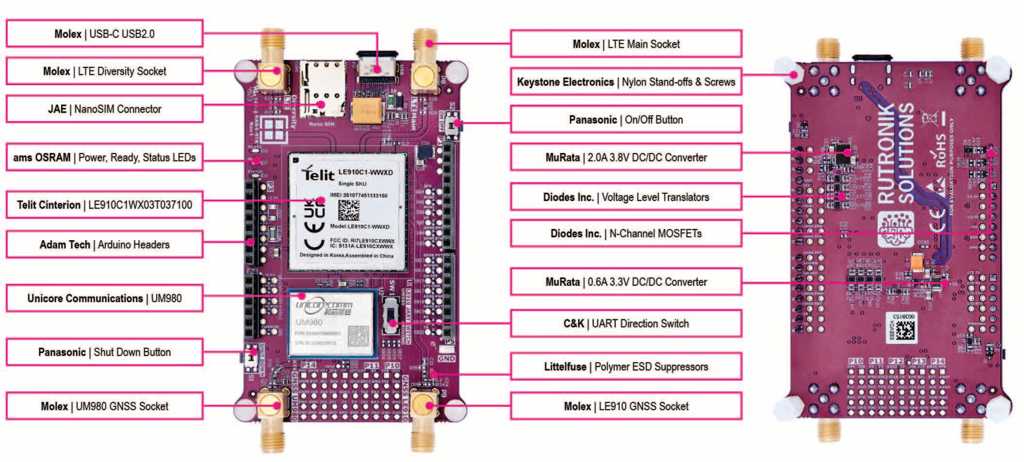


More than 20 years of tremendous effort and an evolution of many different technologies is radically changing the face of today’s smart home.


 Author: Josh Mickolio Supplier Business Development Manager, Wireless and IoT DigiKey
We all have one or multiple favorite smart home ecosystem(s), which may be from Apple, Amazon, Google, Samsung or the many other options available. Having so many options available is usually a great thing, unless you are a company developing for and maintaining all those options. Matter now allows these companies to design one product, i.e. a wireless light bulb, that will now be compatible with all of these popular smart home platforms. With Matter, and you may have noticed this already by searching for Matter keywords online, searches may or may not return your desired results.
The cloud of confusion around smart home development was greatly reduced with the introduction of Matter, a new technology standard introduced by the Connectivity Standards Alliance (CSA). If you have ever shopped for devices to make your home a little smarter, you may appreciate the impact Matter is having on the smart home industry.
My search on some popular search engines for “Matter Starter Kit” returned mostly results for some role-playing games. We thought it would be useful to put together a brief introduction to Matter-compatible devices and development kits.
Matter is a an open-source standard managed by the CSA, and as with most standards organizations, like the Wi-Fi Alliance, Bluetooth SIG and others, the CSA does a great job highlighting devices that are certified for use with Matter.
The CSA website has a host of resources, FAQ, documentation and more at: https://csa-iot.org/all-solutions/matter.
The CSA has a certified products search on their website, located at https://csa-iot.org/ csa-iot_products. On this page you will find two areas, one is a search for end products and the other for compliant platforms. In addition, the “Program Type” filter on the left of the certified products search page lists all of the technologies supported by the CSA, one of which is Matter. A few Matter-compliant suppliers and products are listed below. Please note that this is not a complete listing as there are other variants of these devices available not to mention other companies who utilized these chips in their modules, devices, etc.


Another extremely useful reference is the Project CHIP (Matter) github. There are a lot of examples here for your coding pleasure.
When developing a Matter compliant project, you will find a lot of things remain the same including needing the coding for connectivity and sensors. Where this will vary is that you now need to include Matter as well.
By utilizing one of the many examples referenced above you will be able to save yourself a great deal of time. There are a multitude of different language examples available including, but not limited to C++, Java, and Python, making this a great option for any developer.
When Matter was developed, there were many things that were important to consider, but three key factors were reliability, security, and seamless integration.
These factors continually improve as new versions are released. Some of the key security factors include, device-unique joining authentication, secure over-the-air updates, and network-wide privacy and integrity. By utilizing the resources listed above, a developer can ensure that these security measures and many more are incorporated into their project. To see more on security in Matter, please visit: https://csa-iot.org/resources/security.
The goal of the Matter technology standard is to unify and simplify smart home devices and it came together as part of a highly collaborative effort, three years in the making, between a standards alliance and industry giants. However, if we look deeper into Matter, we can start to appreciate it for what it is, 20+ years of tremendous effort and an evolution of many different technologies that is radically changing the face of today’s smart home.
To learn more and get started with Matter visit: digikey.com/matter

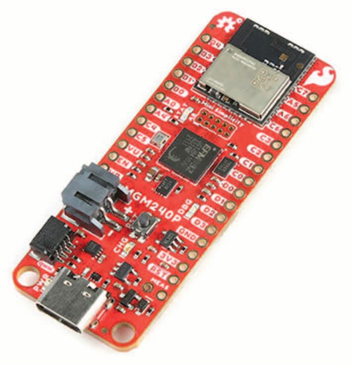
DigiKey is both the leader and continuous innovator in the high service distribution of electronic components and automation products worldwide, providing more than 17.2 million components from over 2,800 quality name-brand manufacturers.
■ DigiKey
www.digikey.com

Texas
Microchip
STMicro
NXP IOTZTB-DK006 Matter Thread Development Kit based on K32W041/061
NXP OM15080-K32W Matter USB Dongle (Can be used as Thread Border Router)
Espressif ESP32-C3-DEVKITM-1 Matter Wi-Fi/Thread Evaluation Board with ESP32
Sparkfun DEV-20270 Evaluation Board, based on MGM240P from Silicon Labs
Silicon Labs XG24-PK6009A Matter Thread Evaluation Board for EFR32MG24
Nordic Semiconductor THINGY53 Matter Thread Evaluation Kit
Silicon Labs RS9116X-SB-EVK2 Matter Wi-Fi/Thread Evaluation Board with RS9116
Infineon CY8CKIT-062S2-43012 Matter Wi-Fi Eval Board for PSOC 6 and CYW43012

Clearly the time is right for ‘Right to Repair’ to be addressed, initially for consumer products that are the visible part of the iceberg, forming part of the much bigger problem of changing our way of working and dealing with the issue of prolonging the lifetime of equipment whilst developing a circular economy. Many business segments will be highly influenced by the new European Directives and will need to figure out new ways to deal with obsolescence.
So how will the power supply industry embrace this change and how could it contribute to prolonging the lifetime of equipments and to reduce waste?
As announced in the EU Circular Economy Action Plan, the Commission has proposed new rules to make almost all physical goods on the EU market more environmentally friendly, circular, and energy efficient throughout their whole lifecycle from the design phase through their daily use, repurposing, and end-of-life.
As part of the Action Plan dated June 2023 the Environment Committee put forward a proposal to make products in the EU ready for those conditions by developing a strategy to prolong the lifetime of equipments and to protect consumers.
The European Ecodesign is well known for energy related issues such as energy efficiency and standby energy consumption, and many detailed articles have been written on this topic. As one of the key elements of the European Green Deal strategy there is another, less well known aspect to Ecodesign that’s about reducing waste and granting consumers the ‘Right to Repair’ thus prolonging the lifetime of equipment.
An important part of this proposal is to set common rules promoting the repair of goods, advancing towards the objective of sustainable consumption under the European Green Deal (Figure 1).
Developing a repair approach will reduce e-waste and reduce the environmental impact, resulting in significant savings for consumers and all of society. As part of that and similar to how it is for Ecodesign

energy consumption labeling, France has proposed the use of a similar label bearing a reparability index to inform consumers about the possibility of repairing a product whilst consumers should have access to repair guidelines.
As proposed in the scope of the project, on December 4 2023 the European Parliament and Council provisionally agreed an update to the ‘ecodesign’ rules, aiming to improve various aspects of products throughout their lifecycle to make them more durable, reliable, easier to reuse, upgrade, repair and recycle, use less resources and energy and water.
The proposal covers consumer goods and concerns defects that may occur in them, whether or not still under legal guarantee. The producer will have an obligation to repair goods for five to ten years after they were purchased. Goods for which reparability requirements currently exist include household products such as washing machines, washer-dryers, dishwashers, refrigeration appliances, electronic displays, welding equipment, vacuum cleaners, and servers and data storage. Mobile phones, cordless phones and tablets are also listed in the recent draft, and EV chargers have been considered in the latest discussions. All of these products use power supplies and manufacturers need to keep future legislation and regulations in mind and monitor their evolution.
This introduction may appear to give the impression that it’s mostly the consumer segment that will be the subject of future legislation but in fact, inspired by the Ecodesign workgroup a lot of activities are taking place within industry to prolong lifetime and this is where it becomes an interesting area for the power supplies industry.
Regarding consumer applications for power supplies, they are either built-in the equipment and part of the overall system, or external such as USB chargers, and the legislator is working on a classification of the level of reparability in making it environmentally and economically a good idea to repair instead of replace. This is part of the 2024 workgroup that is working in parallel with the industry to define reasonable classifications for the benefit of end users and the environment.
Considering the high levels of integration and current building practices, e.g., the use of sealed plastic products such as external adapters, these may not be classified as repairable but the manufacturers might still have the obligation to guarantee support and service for ten years. Also, for embedded power supplies to listed equipments power supplies, manufacturers will be obliged to guarantee the availability of spare parts during the service period.
At higher power levels, as for the energy consumption Ecodesign regulation, servers and data storage are already included in the proposition, and power supplies manufacturers are working in close cooperation with the European representatives to develop power solutions meeting the reparability needs, but also to guarantee longer life time in operation.
maintenance, and when end of life arrives, recycling. For many designers it will be a new way of working but for those used to developing power solutions for refurbishing and system modernization it’s nothing really new and a lot of the best practices deployed in this industry are already meeting future Ecodesign regulations.
BEFORE ECODESIGN REGULATION, REUSE, REPAIR AND PROLONG LIFETIME WAS ALREADY THE NORM IN THE RAILWAY INDUSTRY!
Outside of what the Ecodesign is aiming for in consumer segments, many industrial applications require power supplies manufacturers to provide power solutions for refurbishing and systems modernization. Among many, the transport industry and especially the railway are the
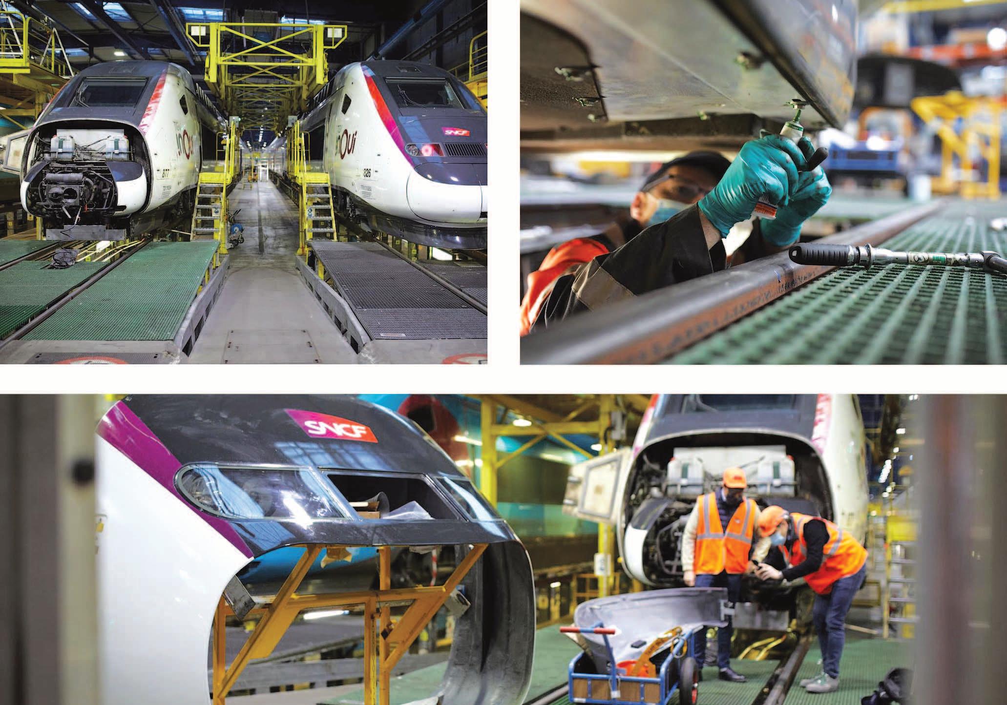
When considering the circular economy, up to 80% of a product’s environmental impact can be determined at the design phase. When designing a power supply for a datacenter we always take into consideration energy efficiency, and power designers use the latest technologies such as Wide Bandgap Semiconductors in order to deliver the highest levels of performance. Regarding prolonging lifetime there is a lot of work going on to select components able to keep their original performance for more than ten years in operational conditions, but designers must also include reparability in the mechanical design, which could imply a modular concept easing
best examples to illustrate what might be applicable to other segments when it comes to Reuse, Repair and Prolonging Lifetime.
One good example is the French railway state-owned operator, ‘Société National des Chemins de Fer (SNCF)’, which in September 2023 announced that as part of its commitment to sustainability, SNCF Voyageurs and its Rolling Stock Division are committed to optimizing the use and lifespan of their trains at every stage of their life cycle: mid-life and end-of-life refurbishment to extend their service life and combat obsolescence, and recycling and reuse of spare parts, etc.
To achieve that goal, the SNCF has announced the commencement of a major refurbishing project to restore and upgrade 104 high speed trains, ‘Trains à Grande Vitesse (TGV)’ to “combat obsolescence” (Figure 2).
These 104 eligible trainsets have been assessed during the 4th quarter of 2023 and 1st quarter of 2024. A number of criteria will be taken into account when deciding the fate of each train set, including the condition of the structure of the train set, its metal components, the boiler, the bogies and the electrical installations including power supplies. Based on these criteria, the trainsets will be classified into three categories:
1 Those in perfect condition that will continue to be in service, but will undergo renovation to improve their comfort.
2 Those that require more extensive reliability and renovation work due to their advanced age.
3 Those that will be withdrawn from service due to obsolescence of parts (electronic components or state of the chassis). These written-off trainsets will be used as parts banks as they contain up to 3,000 potentially recoverable components that can be reused to repair other trainsets.
The SNCF refurbishing project very much illustrates within an industrial environment what Ecodesign Reuse, Repair and Prolong Lifetime is aiming for.
Reusing parts to reduce waste and optimize resources has been part of the SNCF life cycle process for a long time as rather than buying new, checking and repairing 500,000 TGV spare parts every year represents a saving of half a billion euros a year.
The variety of power supplies required by railway companies when refurbishing trains is very wide and covers from low power modules to high power converters up to hundreds of kilowatts (Figure 3).
In a train, many power supplies are embedded within sub-assemblies e.g., LED lighting with built-in power supplies and drivers, but a number of systems require standalone power solutions meeting the latest legislative requirements.
In general, refurbishing contractors are using referenced part numbers approved by the train manufacturers, and about 80% of the need is available as Commercial off-theshelf (COTS) from certified power supplies manufacturers, complying with railways standards.
However, when refurbishing and modernizing trains that might have been manufactured decades ago, 20% of the power supplies will require extra features, higher power density, lower energy consumption and many more things, often with the need to fit into an existing box that’s specific to the application (Figure 4).
When refurbishing or modernizing, the railway industry is following the same pattern as the others, and with the increased demand for higher power density and lower power consumption, power designers are now investigating the implementation of Wide Bandgap (WBG) switching semiconductors, Gallium Nitride (GaN) and Silicon Carbide (SiC). SiC diodes have been used in railway power supplies for decades, but power switching transistors are relatively new in railway applications.
Considering that the lifetime of railway equipment could be greater than 20 years, reliability and supply chain sustainability are a must, and implementing a new technology requires a thorough technical evaluation and the need to ensure that the supply chain is able to guarantee product support for more than 20 years.
In high power switching conversion many projects utilize SiC MOSFETs instead of IGBTs and it’s worth mentioning the Fraunhofer Institute for Energy Economics and Energy System Technology’s MUSiCel research project which by using innovative SiC wide-band-gap semiconductors managed to deliver 250 kW at a switching frequency of 50 kHz with an efficiency across the entire power range exceeding 98 % (at 100 kW, an efficiency of even 98.8% was measured!) (Figure 5).
Originally the MUSiCel research project was aimed at the electrification of agricultural and construction machinery, although it can equally apply to railway high power conversion systems and there’s no doubt that such research will contribute to the adoption of SiC in future designs.
The WBG supply chain for SiC and GaN is now entering a mature phase, thus securing a much needed long term components availability situation.
To the question: Ecodesign, Reuse, Repair, Prolonging Lifetime and New Technology
– Is it the new paradox? The answer is not “Yes” or “No” but as for the railway industry we have given as an example, industry as a whole will have to consider all those aspects when designing new products. The EU Ecodesign is setting a new way of working, and from higher energy efficiency to prolonging the lifetime of final equipments, power electronics will play an important role. One thing is for certain, it is a wonderful opportunity for power designers to explore new frontiers.
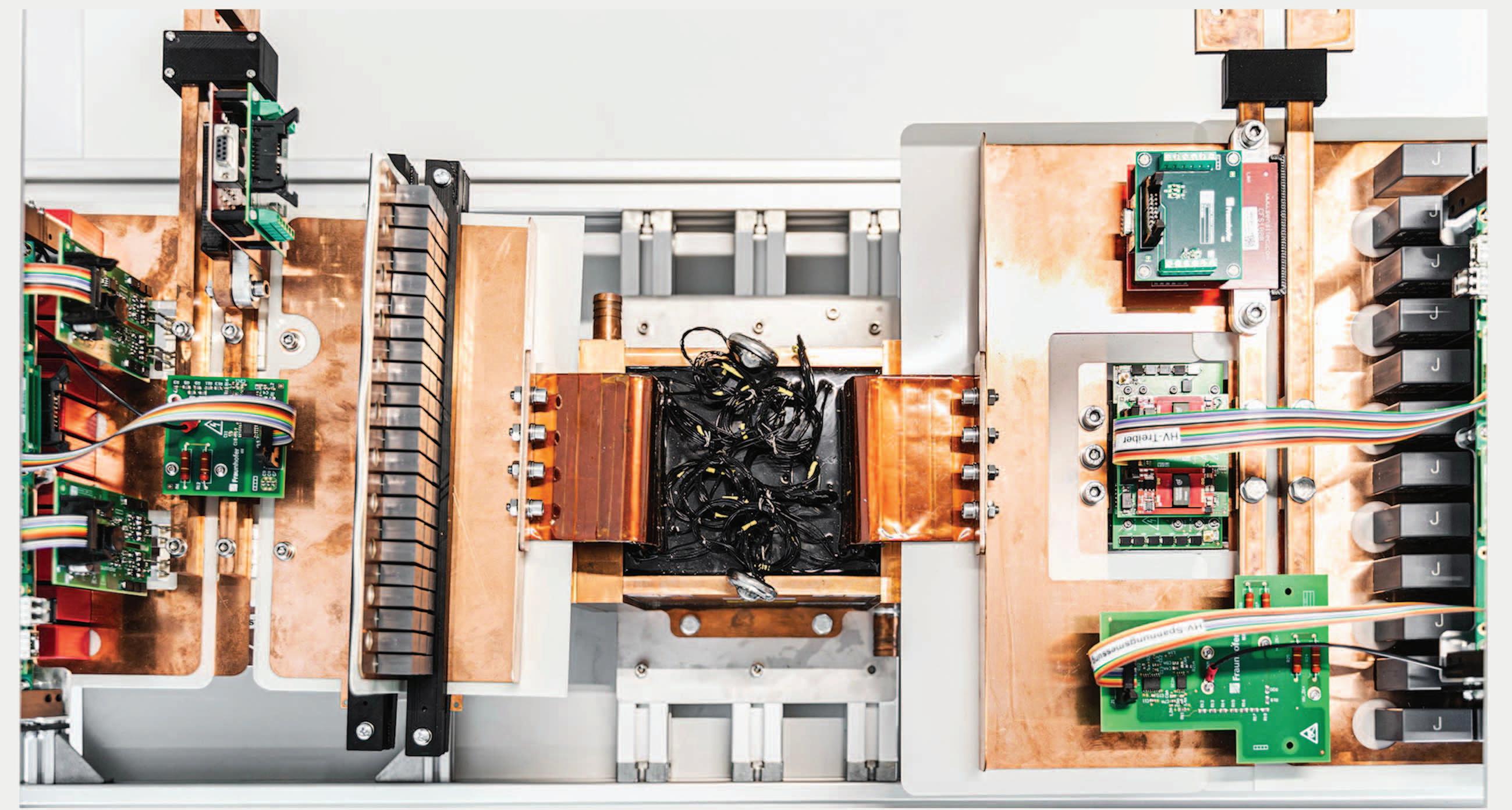
In the process of validating a new technology for highly demanding railway applications, the parallel, ongoing process to electrify other transportation and machinery applications is contributing to accelerate market adoption and confidence in WBG and especially SiC. A lot of research has been conducted by the automotive industry to validate WBG technology and the adoption of SiC and GaN in powertrains and battery chargers thus setting a ground base for other segments to adopt the technology.
The research of feasibility, reliability and benefits compared to previous technologies is very important, but for railway manufacturers it is crucial that long term supply chain sustainability is guaranteed for the lifetime of the final equipment.
As it was for MOSFET technology, WBG semiconductors manufacturers have invested in volume manufacturing facilities or partnerships, but we also see a number of acquisitions e.g., Infineon acquiring GaN Systems, and Renesas acquiring Transphorm.
References:
Powerbox (PRBX): https://www.prbx.com
Ecochain: https://ecochain.com
SNCF: https://www.sncf.com/en
Fraunhofer IEE: https://www.iee.fraunhofer.de/en.html
■ Powerbox (PRBX) www.prbx.com


Würth Elektronik eiSos made its return to the prestigious Applied Power and Electronics Conference (APEC) held in Long Beach, California, USA, in February 2024. With a history spanning over 35 years, APEC has solidified its position as the premier showcase for electronic components in North America. Prior to the exhibition, technical minds met at the PSMA/PELS Power Magnetics workshop, where Würth Elektronik displayed a strong presence.
At APEC, George Slama, Senior Application and Content Engineer at Würth Elektronik, assumed the role of Session Chair for Industry Sessions such as “Modeling and Simulation of Magnetics – Closing the Loop” and “EMI & Magnetics.” Slama also reprised his role as Technical Dialog Session Chair for “High Frequency Magnetics” and “Magnetic Design & Optimization” sessions. Slama displayed his technical knowledge during an Exhibitor Presentation as he hosted “Advancements in EMC Filter and Component Selection Tool” during the exhibition.
Also representing the company, Matt Wilkowski, Design Consultant for Würth Elektronik, served as Technical Dialogue Session Chair for Tuesday’s “High Frequency Magnetics” and “Magnetics Applications II” sessions, along with being the Technical Lecture Session Chair for “Magnetics & Modeling Simulation” and “Magnetics Applications I” on Thursday.
During the conference, Würth Elektronik’s Global Business Consultant, Lorandt Foelkel, delivered an Industry Session titled “See the Power of IoT in Action! Live, Functional Demo of Solutions.”
Additionally, seasoned Application Engineer Jared Quenzer hosted a Professional Education Seminar, “EMC Workshop for Power Supply Designers,” which kicked off the week on Sunday, February 25.
The Booth
During the show, Würth Elektronik released the newest edition of their guidebook; “The Trilogy of Wireless Power Transfer 2nd edition.” Cem Som, author of the guidebook, was available on the booth to answer technical questions and offer support.
Now a cult:


Also released in Long Beach is Würth Elektronik’s comprehensive manual, “DC/DC Handbook.”
“Our more-than-you-expect service was and is the foundation of Würth Elektronik’s corporate success,” confirms Alexander Gerfer, CTO of the Würth Elektronik eiSos Group, a well-known component manufacturer . “Our DC/DC Converter Handbook, which we presented for the first time at the conference, proves that we are serious about promoting innovation and knowledge transfer. True to our mission “creating together”, we will continue to ensure that great ideas get the right power – through functional power supplies as well as targeted development support, especially for start-ups.”
Throughout the duration of the exhibition, Würth Elektronik showcased a variety of partner demonstrations on their distinctive booth. Highlighted activities included an interactive 50W WPC Shuffleboard table in collaboration with Infineon Technology, a miniature Ferris Wheel powered by a 24V Brushless DC Motor featuring customizable LED lighting in partnership with Renesas, and an engaging bean bag demonstration game showcasing Texas Instruments Power and Motor Control Solutions.
Attendees who actively participated in the booth’s interactive activities received a complimentary pair of Würth Elektronik branded socks and were entered for a chance to win a pair of Apple Air Pods.
In addition to exploring the interactive exhibits, APEC attendees had the opportunity to engage in technical discussions

with Würth Elektronik experts, receive the iconic Würth Elektronik APEC hat, and secure an exclusive invitation to one of the exhibition’s premier events: the highly anticipated Tuesday Night Party hosted by Würth Elektronik.
Würth Elektronik eiSos www.we-online.com

vCharM.edge hardware
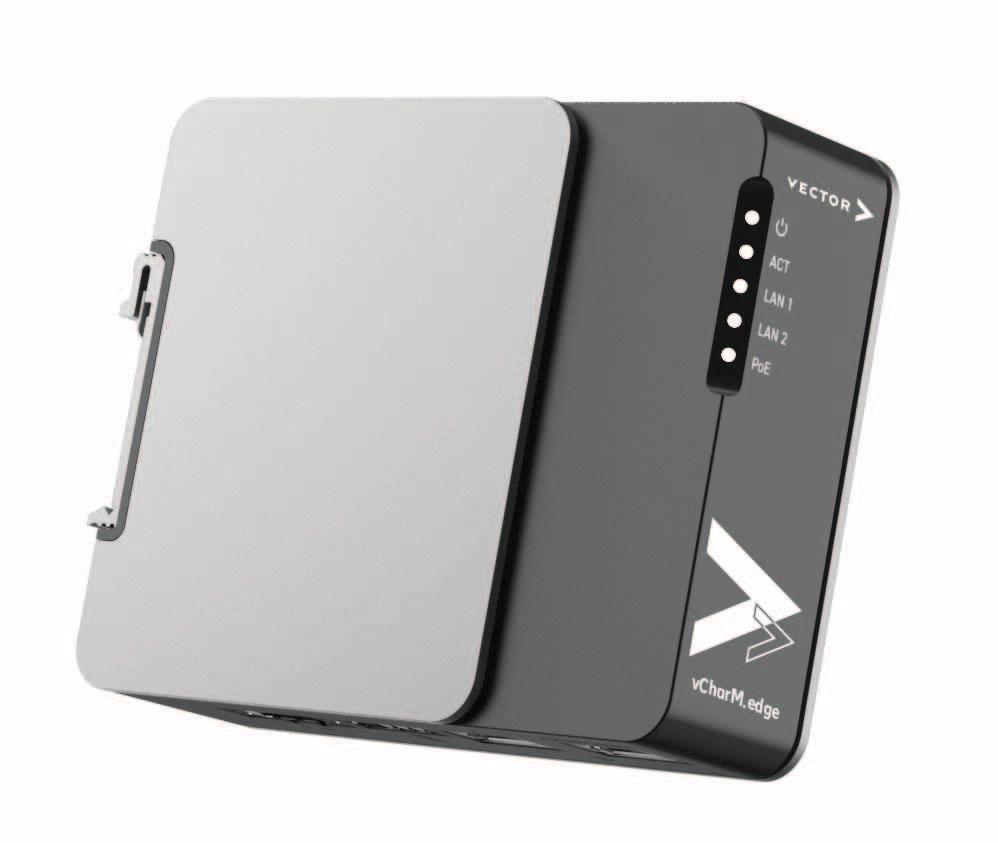
Vector Informatik is expanding its product portfolio in the field of e-mobility charging infrastructure with the vCharM.edge hardware. Operators of charging parks can use it to implement dynamic load management. This avoids expensive grid expansions and still guarantees full charging without expensive peak loads for all vehicles.
vCharM.edge is a hardware that is installed locally in the charging park. Here, it connects to the charging and load management tool vCharM from Vector, which runs in the cloud. At the same time, vCharM.edge communicates with the local charging stations via OCPP and receives the building’s energy consumption via an energy meter. Based on these values, the remaining available energy is continuously provided to the charging infrastructure. For the end customer, this means more efficient and cost-effective charging processes compared to static load management. Settings and reports are still easily made and viewed via the cloud in vCharM. Another advantage of running charging and load management locally is offline authorization. Even if the internet connection to vCharM fails, the electric vehicles are charged at the charging stations as the most important parameters are stored in vCharM.edge. Authentication takes place as usual via RFID cards, key codes or Autocharge.
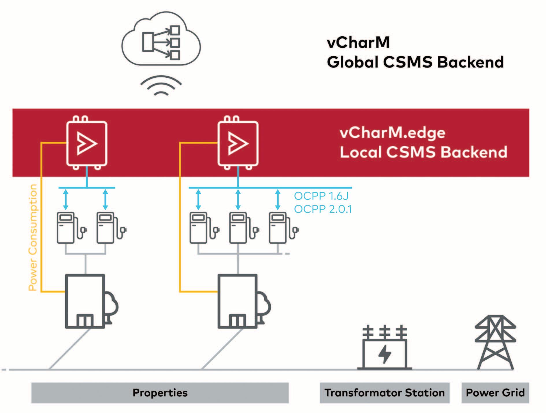
vCharM.edge receives the power consumption of the property in order to increase or reduce the charging power depending on this. This ensures that the installed power of the property is utilized in the best possible way.
Further information on vCharM.edge can be found at: www.vector.com/vcharmedge
■ Vector | www.vector.com

The company’s experts will be showcasing automotive software development tools at booth 255 in hall 4.
TASKING will be presenting its latest tools for the development of high-performance, safe and secure embedded automotive software at embedded world 2024 in Nuremberg from April 9 to 11, 2024. At booth 255 in hall 4, TASKING will be presenting its wide range of tools that span the complete software development process, known as “Compile, Debug, Analyze”.
Author: Bernd Hantsche Vice President Product Marketing Embedded & Wireless RutronikOne of TASKING’s pillars of success is its focus on safety and security-compliant development. The company’s certified tools, aligned with ISO 26262 and ISO 21434 standards, empower designers to fast-track their software development while maintaining compliance. A current industry trend is test automation, and how the use of CI environments and test automation farms can drastically improve the efficiency of the development process. TASKING’s experts will demonstrate how the iC7mini and other versions of the BlueBox can turn this into a reality.
TASKING WILL HAVE FOUR DEMOS AT THE BOOTH:
• Workstation 1 will showcase a battery management system designed by TASKING’s partner Neutron Controls that is based on an AURIX™ TC4x microcontroller from Infineon Technologies. The demo will highlight the newest release of the SmartCode Integrated Development Environment Toolset and the BlueBox hardware debugger iC7mini.

• Workstation 2 will show a simple application running on the NXP S32Z270A that was built on the recently released VXToolset for ARMv7.0, which provides support for NXP® Semiconductor’s S32Z and S32E real-time processors with Arm® Cortex®-R52 architecture.
• Workstation 3 highlights TASKING’s RISC-V tool support. The RISC-V tools enable compilation, verification, debugging, performance tuning, timing analysis, and coverage analysis for software running on multi-core, multi-hart SoCs. The tools are demonstrated using Andes’ ISO 26262-certified RISC V processor IPs and associated MachineWare Virtual Models. This demo will also be shown at the upcoming Andes RISC V Conferences in Taiwan, China and Japan.

• Finally at Workstation 4, TASKING together with Vector will demonstrate ARTI-based AUTOSAR Profiling with Vector MICROSAR Classic on a TC399XE Eval Board as well as a virtual ECU, using a Synopsys TC39x VDK. winIDEA enables the execution of trace-based timing tests on both real and virtual targets without changes to the test environment, such as test scripts or third-party tools.
In addition to the demos, TASKING will be presenting two technical topics during the embedded world conference. On 10 April at 4 p.m., Gerard Vink, Industry Specialist at TASKING, will speak on “Power and Energy Dissipation Aware Compiler Optimizations” about how the design and implementation of software affects the energy consumption of embedded systems. On the same day, at 5 p.m., Markus Krahl will address the topic “An Industrial Case Study on Formal Verification of Embedded C-Code Using Open-Source Tools”. In his presentation, he will examine the suitability of tools for formal methods to improve the overall quality of embedded C code, particularly with regard to security and protection functions.
TriLite announces availability of form factor engineering samples for Trixel® 3 Laser Beam Scanner (LBS), to accelerate development of AR use cases
TriLite announces that form factor engineering samples for its Trixel® 3 laser beam scanner (LBS) are now available, combining the display engine, control electronics and TriLite’s unique Trajectory Control Module (TCM) software. By providing all the system-level components required for evaluation, application development and test, these samples will enable customers to rapidly prototype their augmented reality (AR) systems and cut time-to-market.
Trixel 3 is the world’s smallest projection display. It provides ground-breaking compactness and light weight, coupled with exceptional brightness and accuracy. It enables AR solutions for smart glasses and a wide range of consumer applications, with ultra-low power consumption (<320 mW) for all-day use. The engineering samples are based around the Trixel 3 optical display engine, which combines a single 2D MEMS mirror, RGB laser diodes and all optical components. The LBS unit is supplied pre-calibrated for color alignment and distortion correction. The display engine and the driving electronics are now form factor, which is important for customers to rapidly design and prototype their AR systems leveraging Trixel 3 technology.
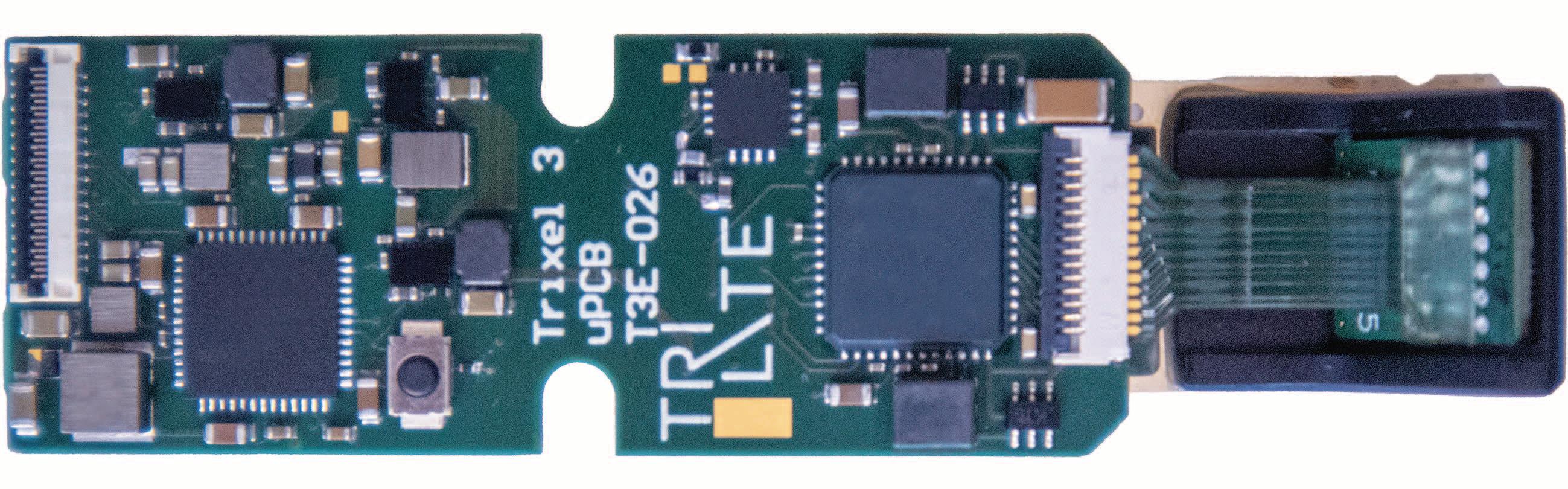
TriLite’s latest TCM software is supplied with the engineering samples. TCM is part of TriLite’s ‘software-defined display’ approach, which shifts complexity from the hardware to the software domain. It uses proprietary algorithms to ensure optimum image quality and minimum latency, control position and brightness at subpixel accuracy, and to assure low power consumption. TCM runs on a host processor, and the engineering samples include a suitable evaluation host.
The engineering samples also include driving electronics for connecting the Trixel 3 LBS to the host. This includes the TriLite Image Controller (TIC), and drivers for the RGB laser diodes and the MEMS mirror.
Trixel 3 is fully compatible with state-of-the-art waveguides without requiring any relay optics, thus saving space and reducing weight.
■ TASKING Germany GmbH | www.tasking.com
The Dfinity Foundation is focused on defining and introducing the Internet Computer Protocol.
■ TriLite | www.trilite-tech.com
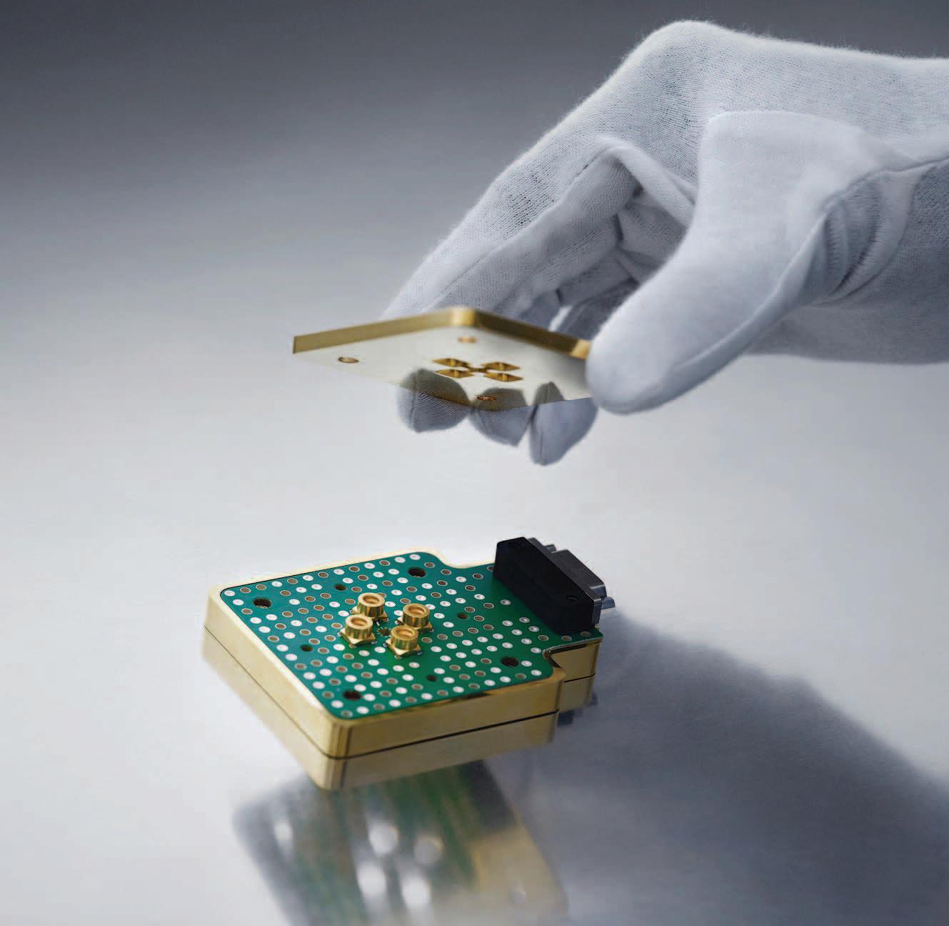
SemiQon
SemiQon, a Finland-based startup specializing in silicon-based quantum processors, has announced it has successfully manufactured and pre-tested a 4-qubit quantum dot array from the first production run at its manufacturing facility in Espoo, Finland. The new chips are now shipping to strategic partners around the world as a toolkit for further research and development. The aim is to help make building stable logical qubits easier and faster to accelerate the use of quantum computing for complex problems. First-generation quantum computers have already achieved impressive computational feats. However, solving highly specific problems related to pharmaceuticals, logistics, space, and material design will require increased computational power. As researchers, ecosystems, and companies around the globe lay out their ambitious visions for quantum computing, the computing power must still be scaled efficiently to address these challenges. Current methods do not make this possible.
“We are gradually moving towards the million qubit era and the contribution of hardware is becoming more and more essential,” says Dr. Himadri Majumdar, CEO and Co-founder of SemiQon. “Our solution builds on the technological development and knowhow of semiconductors and benefits from existing infrastructure and industry. Utilizing such infrastructure effectively and efficiently has allowed us to accomplish one of our first goals within a short period of time. The challenge is getting to quantum supremacy in a sustainable, scalable, and affordable manner. These new chips are our first step in a long journey to making quantum dreams a reality.”
SemiQon’s strategic path of combining classical and quantum elements at cryogenic temperatures also took a big leap forward through the demonstration of very low noise and better control over the channel using record low sub-threshold swing in the manufactured fully-depleted silicon-on-insulator metalon-semiconductor (FDSOI-MOS) transistors. These transistors will be the backbone of realizing a cryogenic integrated circuit (IC), ultimately leading to quantum IC for scalable, efficient, and affordable quantum computers.
The results will be communicated through a peer-reviewed international scientific article, which is currently under review.
Since the launch of its production chip manufacturing line last year in the Micronova Center for Applied Micro and Nanotechnology in Espoo, SemiQon has established several university and commercial partnerships with organizations looking to move quantum computing closer to its goal of usable physical and logical qubits. The first-generation SemiQon chips are already shipped to strategic partners globally for further testing and experimentation, mainly for the advancement of research and development in the domain.
“SemiQon’s prototype devices and their proposed fast iteration of the new generation of devices are beneficial and necessary for the research community to experiment on and push the boundary of public research,” says Professor Dominik Zumbühl of the University of Basel in Switzerland, one of SemiQon’s strategic collaborators.
SemiQon will be attending the Quantum.tech USA event in Washington DC, USA, in April 2024, where they will share SemiQon’s vision and mission for their cost-efficient advancements in quantum chip manufacturing.
SemiQon works closely with the quantum ecosystem from research groups to full-stack companies and is actively discussing with more partners to bring scalable quantum computing solutions to reality.
■ SemiQon | www.semiqon.tech
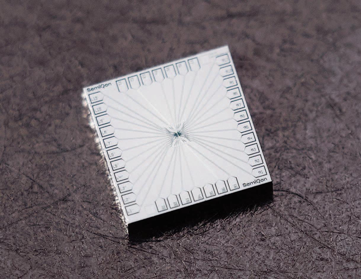
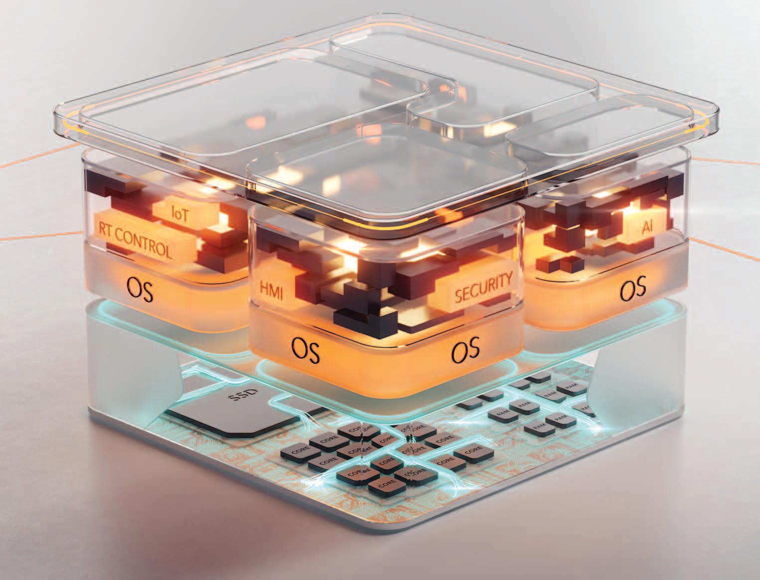
The goal: Fitting computeron-modules with everything that application developers need
congatec launches new product family aReady.COM, the first key stage of its innovative aReady. strategy, which offers significantly smoother implementation of embedded and edge computing technology with the assistance of high-performance embedded building blocks, ranging from Computer-on-Modules (COM) to cloud. congatec’s new aReady.COMs integrate application-ready hypervisor, operating system and IIoT software configurations that customers can put together according to their individual requirements. Developers can boot these individually configured aReady.COMs straight away and then install their applications. This means that the complexity of the integration work below the application layers and for the diverse IIoT functionalities of an embedded and edge computing system is reduced to a minimum. The first aReady.COMs are available with the ctrlX OS from Bosch Rexroth. More aReady. products are to follow.
For customers, aReady.COMs mean that they can count on computer-on-modules in a function-validated complete package, the application-readiness of which extends to the virtualisation, OS, and software layer, to which OEMs can seamlessly connect their applications.
aReady.COMs decouple system development from application development to the highest degree, resulting in significantly faster time-to-market because OEMs can focus completely on application development.
“Our aReady. strategy is congatec’s innovative approach for simplifying the implementation and use of modern basic technologies over the entire life cycle of customer applications. This will raise “application-readiness” as a mark of quality to a whole new level. Moreover, it is not just limited to COMs but even covers everything from COM to cloud. Computer-on-modules from congatec and all the services that we offer for it have always been geared towards making the integration of our embedded and edge computing technologies as easy as possible for developers. Our aReady.COM means that we are establishing a new premium level for this application readiness. It makes the use of our modules even more convenient and efficient, because the software building blocks required, both below and alongside the customer application are provided by congatec in application-ready form in the required configuration and function-validation,” explains Tim Henrichs, Vice President Marketing & Business Development at congatec
“The seamless integration of our hypervisor technology, and our growing portfolio of industrial software along with the integration of operating systems such as ctrlX OS, represent the first key stage of our aReady. strategy. Our roadmap also includes a whole host of further fully configurable, application-ready hardware, software and service building blocks, covering everything up to cloud solutions for device management and maintenance. The most important point about all these aReady. products is that they will be an integral component of computer-on-modules, are fully functionvalidated and are pre-configured to individual requirements from a single source. This kind of comprehensive portfolio for system design can otherwise only be found in dedicated solutions at system level. What we are doing, though, is positioning this solution portfolio much earlier in the value-added chain and therefore making it available for the entire community of embedded and edge computing developers,” explains Andreas Bergbauer, Manager Solution Management at congatec.
The feature set in detail
In terms of hardware, application-ready aReady.COMs offer a hypervisor integrated in the firmware and an integrated memory on which the operating system(s) and IIoT applications are pre-installed to individual requirements. If, for example, the Linux-based ctrlX OS operating system from Bosch Rexroth is used, the entire ctrlX OS World is also opened up automatically, along with the extensive app portfolio of the ctrlX Store for PLC applications, motion control and communication, as well as engineering tools. Developers can also access a wide range of IoT and cloud apps, including key functions such as firewalls and VPN clients.
For the evaluation of the aReady.COM portfolio, customers can currently choose between two computer-on-modules on the basis of the COM-HPC standard: The COM-HPC conga-aCOM/mRLP Mini Module and the performance-oriented COM-HPC conga-aCOM/cRLP Client Size C Module, both based on the 13th Generation Intel Core processor series (code name “Raptor Lake”). More information from congatec: https://www.congatec.com/en/aready/ Visit congatec in Hall 3 at Stand 241. congatec
www.congatec.com

Navitas Semiconductor has announced their AI data center technology roadmap for up to 3x power increase to support similar exponential growth in AI power demands expected in just the next 12-18 months.
Traditional CPUs require typically only 300W and the data center ac/dc power supplies would typically power the equivalent of 10 of these or 3,000W (3kW). High-performance AI processors like NVIDIA’s ‘Grace Hopper’ H100 are already demanding 700W each today, with next-gen ‘Blackwell’ B100 & B200 chips anticipated to increase to 1,000W or more by next year. To meet this exponential power increase, Navitas is developing server power platforms which rapidly increase from 3kW to up to 10kW.
In August 2023, Navitas introduced a 3.2kW data center power platform utilizing latest GaN technology enabling over 100W/in3 and over 96.5% efficiency. Now, Navitas is releasing a 4.5kW platform enabled by a combination of GaN and SiC to push densities over 130W/in3 and efficiencies over 97%. These two platforms have already generated significant market interest with over 20 data center customer projects in development expected to drive millions in GaN or SiC revenues starting this year.
Navitas also announced its plans to introduce an 8-10kW power platform by the end of 2024 to support 2025 AI power requirements. The platform will utilize newer GaN and SiC technologies and further advances in architecture to set all-new industry standards in power density, efficiency and time-to-market. Navitas is already engaged with major data-center customers, with full platform launch anticipated in Q4 ’24, completing this 3x increase in power demands in only 12-18 months.
Navitas’ unique data-center design center is creating these system designs to address the dramatic increases in AI data center power requirements, and assist customers to deploy platforms quickly and effectively to meet the accelerated time-to-market demands of rapid AI advances. System designs include complete design collateral with fully-tested hardware, schematics, bill-of-materials, layout, simulation and hardware test results to maximize first-time-right designs and fast revenue generation.
■ Navitas Semiconductor | www.navitassemi.com

MikroElektronika (MIKROE), the embedded solutions company that dramatically cuts development time by providing innovative hardware and software products based on proven standards, today announced a Click Shield for the Red Pitaya engineering platform. Red Pitaya is an opensource software-defined instrument and an FPGA development tool, often referred to as engineering’s ‘Swiss Army Penknife’. The size of a credit card, Red Pitaya combines the functionalities of multiple lab instruments –oscilloscope, signal generator, and spectrum analyzer –with ample programming capabilities and open-source software to jumpstart any project. Click shields are adapters that bring Click board™ connectivity to popular development platforms such as Arduino, Raspberry Pi, STM32 Nucleo, and now, Red Pitaya.
Comments Nebojsa Matic, CEO of MIKROE: “This Click Shield is the ideal companion for Red Pitaya, designed to unlock even more possibilities for engineering and programming projects. It facilitates the seamless integration of Click
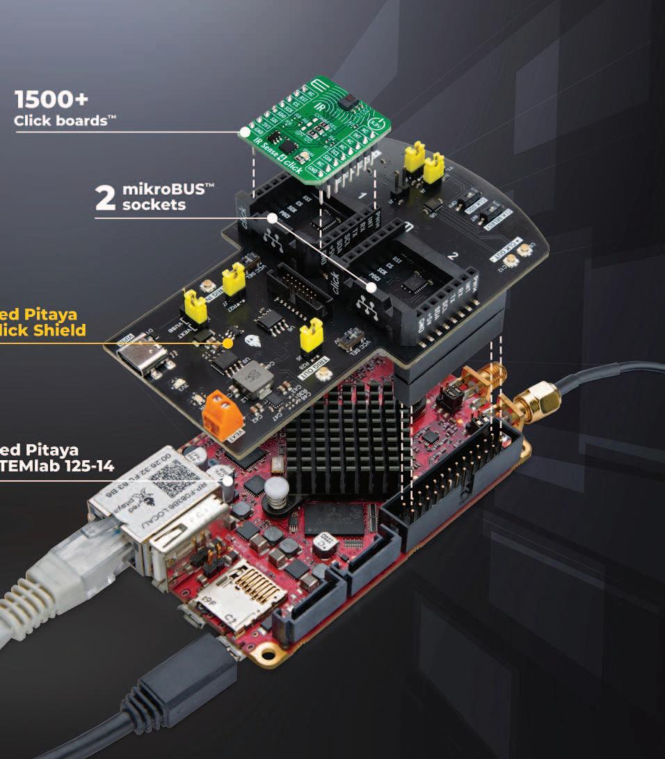
boards with your Red Pitaya host board, expanding its capabilities and versatility. Once the Red Pitaya host board is connected with our Red Pitaya Click Shield, designers can access over 1550 of Click boards, plus a library containing functions and example codes for MIKROE compilers.”
Featuring two mikroBUS sockets, the Red Pitaya Click Shield can be powered through an external power supply, supporting a wide voltage range from 12V to 24V, or via a USB Type C connector, ensuring set-up flexibility. Also, the user is offered the possibility of using any Click board with the help of existing bi-directional level-shifting voltage translators, regardless of whether the Click board operates at a selected 3.3V or 5V logic voltage level.
One distinctive feature of the Click Shield is its shuttle-like connector, purpose-built for Logic Analyzer connection. This connector is your gateway to easily monitoring and analyzing SPI, UART, or I2C signals, providing valuable insights into your projects.
Another remarkable feature is the integration of the ZL40213, an LVDS clock fan-out buffer with two identical output clock drivers. This component is designed to distribute low-jitter reference clocks from external or internal sources, depending on your needs.
Whether for wired or optical communications applications, the Click Shield ensures minimal jitter, maintaining signal integrity. Moreover, it extends its utility beyond clock signals with a dedicated section for trigger signal distribution and synchronization.
■ MikroElektronika | www.mikroe.com

To simplify Automotive and Industrial System Designs
Nexperia introduced a new series of 4- and 8-channel analog switches designed to monitor and protect 1.8V electronic systems. This series of multiplexers includes AEC-Q100 qualified variants intended for use in automotive applications as well as standard versions suitable for a broader range of consumer and industrial applications including sensor monitoring and diagnostics, enterprise computing and domestic appliances. When using analogue switches, designers commonly require additional voltage translators because the control circuitry cannot operate from the voltage level used to supply power to the switch. By contrast, the control pins in the NMUX1308 and NMUX1309 switches operate independently of their power supply voltage range, negating the need to use additional components to perform level-shifting and thus saving board-space and reducing costs.
Nexperia has designed this series of switches to include additional features which enhance overall system safety. Fail-safe logic permits control pins to be biased prior to system powerup and remain biased even after the system has powered down. This eliminates the requirement for power sequencing between the analog switch and the system microcontroller unit (MCU). A power-off protection feature allows analog pins to be biased prior to system power-up and to remain biased after system power-down. This removes the restrictions associated with power sequencing for the analog switch and various power rails which support analog signals and ADC circuitry further down the signal-chain. The combination of both features in the NMUX130X prevents back-power of the supply rail through any pin of the analog switch.
These devices integrate injection current control circuitry, limiting output voltage shifts on the active channel to under 5 mV when an overvoltage event happens on disabled signal channels. This eliminates the need for external diode and resistor networks, saving board-space and reducing cost.
The NMUX1308 and NMUX1309 switches include 8-channel and dual 4-channel devices, in standard (-40°C to +85°C) and automotive-qualified (-40°C to +125°C) versions and are available in leaded and leadless options, including a leadless package which support AOI (Automated Optical Inspection) for automotive applications.
To learn more about Nexperia’s NMUX130X analog switches, visit https://www.nexperia.com/analogswitches
■ Nexperia | www.nexperia.com

Mouser Electronics, Inc., the New Product Introduction (NPI) leader™ empowering innovation, is pleased to announce its sponsorship of the 22nd Create the Future Design Contest, a global challenge to engineers and innovators around the world to design the next great thing for a chance to win the grand prize. Mouser, which has sponsored the contest for over ten years, is joined again by valued manufacturers Intel® and Analog Devices, Inc. (ADI) as co-sponsors. The competition is produced by SAE Media Group, an SAE International Company, and Tech Briefs magazine. COMSOL is also a principal sponsor of the contest.
The contest opens for entries on March 1 and closes on July 1, 2024. The grand prize winner receives worldwide recognition and a cash prize of $25,000 for an innovative product that benefits society and the economy. Previous contests have produced more than 15,000 design ideas from engineers, entrepreneurs and students in more than 100 countries.
“At Mouser, fostering innovation is rooted in our foundation from the company’s earliest days,” said Kevin Hess, Mouser Electronics’ Senior Vice President of Marketing. “We are proud to sponsor programs like the Create the Future Design Contest to support the innovators, inventors, engineers and scientists who will create what’s next in technology.”
The Create the Future Design Contest brings attention to product designs that enhance humanity, improve healthcare quality or help provide sustainable solutions. Previous grand prizewinning entries include self-destroying plastics, a self-contained organ and limb transport device, and an economical, rapid screening device to prevent food-borne illness.
The contest was created in 2002 by the publishers of Tech Briefs magazine to help stimulate and reward engineering innovation. The grand prize winner will be chosen from the winners in seven entry categories: Aerospace and Defence, Automotive/ Transportation, Electronics, Manufacturing and Materials, Medical, Robotics and Automation, and Sustainable Technology.
■ Mouser Electronics | www.mouser.com

Mouser Electronics, Inc., the authorised global distributor with the newest electronic components and industrial automation products, is proud to mark the company’s 60th year in business. Mouser began with a couple of employees working out of a garage in El Cajon, California, and today ranks as a top 10 global distributor and multi-billion-dollar corporation with 4,000 employees and 28 locations worldwide. Much has changed in the electronics industry since 1964, but Mouser has remained dedicated to providing the newest technology to customers as quickly as possible.
Mouser Electronics President and CEO Glenn Smith, who joined the company in 1973, attributes Mouser’s success to the hard work of the Mouser team and its dedication to providing best-in-class service.
“I congratulate all Mouser employees, past and present. We would not be here today without the exceptional teamwork of our people. They are the backbone of our longevity. Each of us continues to play an important role in making our company thrive,” said Smith. “Together, we have accomplished great things, and we are far from finished.”
“I always tell employees that ‘satisfied customers’ made their paychecks possible,” Smith added. “Our customers and manufacturer partners are a big part of Mouser’s success story. We are extremely grateful for their patronage and partnership through the decades.”

A lot has changed since college junior Glenn Smith took a parttime job in the warehouse of what was little more than an electronics startup near San Diego back in the early 1970s. He was one of just 12 employees. Over the past five decades, Smith helped build the small company into the top-10 component distribution giant that Mouser is today, serving over 650,000 customers and distributing the newest semiconductors and electronic components from over 1,200 manufacturer partners.
Mouser has a rich history with many milestones. In 1973, when college junior Glenn Smith took a part-time job in the warehouse, he was one of just 12 employees. In 1986, the company moved its operation from California to Texas, placing Mouser near Dallas/Fort Worth International Airport to expand the company’s distribution capabilities. In 2000, Fort Worth-based TTI, Inc. acquired Mouser, and in 2004, Smith was promoted to President and CEO. In 2007, Mouser and TTI were acquired by the Warren Buffett-owned Berkshire Hathaway, Inc.
Along with its 28 locations, Mouser’s central hub is the company’s global headquarters and distribution centre on its 100-acre campus in Mansfield, Texas. Throughout the decades, Mouser has been recognized for innovation, leadership, and its industry, community and marketing efforts, winning a multitude of awards.
In 2012, Mouser received an Employer of Excellence Award for Tarrant County for significant economic and community impact on North Texas.
In 2019, Smith was named Top Public Company CEO by the Fort Worth Business Press. Mouser also won a 2014 Large Business of the Year Award and a 2021 Best Places to Work Award.
For 2022, the company received more than 30 awards for distribution excellence from its manufacturer partners.
For more information on the 60th Anniversary, please visit https://eu.mouser.com/60years
■ Mouser Electronics | www.mouser.com
The countdown is on – in three months, the trade fair for microelectronics will once again bring people and technologies together in the exhibition halls of Nuremberg, Germany. From 11 – 13 June 2024, the event will offer a platform for experts in electronic assembly and connection technology. A hall connecting the two themes of electronics manufacturing and power electronics, will provide even more opportunities for professional exchange in both fields.
The SMTconnect 2024 offers a new way aspect: In order to increasingly address the interaction between electronics manufacturing and power electronics, Hall 5 of the PCIM Europe will be dedicated to “Smart Power System Integration” as a connecting element between the two industries. This hall will focus on the specific requirements of power electronics manufacturing.
The Future Packaging Production Line by the Fraunhofer Institute for Reliability and Microintegration offers additional insights into individual production steps. This year’s motto is “See the REAL DEAL” and focuses on how a higher degree of digitalization and automation can make manufacturing processes more robust against disruptions and external influences. This networking of experts from both the electronics manufacturing and power electronics sectors enables not only a comprehensive view of the entire production process, but also provides an intensive exchange to develop cross-industry and customized solutions.
Visitors to the SMTconnect 2024 can look forward to a varied program of lectures. On the second day of the trade fair, power electronics production will be the main topic at the forum. The program will be supplemented on all three days by subjects such as “AI in electronics production and Industry 4.0” and “Sustainable electronics production”. Industry experts will present and discuss new solutions and trends in electronics manufacturing. The full forum program will be published on the SMTconnect website from mid-April.
■ SMTconnect | https://smt.mesago.com


When carrying out presence control in automated intralogistics and packaging processes, the job of the sensor system is to safely detect the various objects. Handling of the sensor, including mounting, alignment and adjustment, must also be quick and simple, especially as a large number of sensors often need to be installed. This is why a) standardization and b) adaptation of the sensor to the individual needs of the customer are extremely important for the cost-effective commissioning of a system. We have developed an optimized sensor generation for precisely these requirements:
The new 5B series. Highly economical. Perfect handling.
Advantages for you
■ Housing: New, compact housing (dimensions W × H × L: 11 mm × 32.4 mm × 20 mm) – installation-compatible with previous series – ideal for tight installation spaces. Certified with degree of protection IP 67 and ECOLAB
■ Attachment and mounting: Fast attachment and easy mounting thanks to metal inserts with M3 thread
■ Commissioning: All-around visible 360° indicator LEDs for easy installation and status display. Fast alignment thanks to homogeneous and easily visible light spot
■ Optimal configuration: Easy alignment and adjustment to the application thanks to a user-friendly potentiometer
■ Safe detection of depolarizing objects: Optimized performance for the detection of reflective, shrink-wrapped, and shiny objects
■ Electrical connection: Adaptation to individual customer requirements thanks to different connection options (e.g., cable, M8 connector, pigtail,...)
■ Switching frequency: Improved switching frequency for throughbeam photoelectric sensors with up to 900 Hz for high performance and function reserve
■ Tamper protection: Light/dark switching takes place in a tamperproof manner through polarity reversal of the (cable) wiring
Available operating principles

Retro-reflective photoelectric sensor

Throughbeam photoelectric sensor
Caracteristici
Cost effective mounting

Diffuse sensors
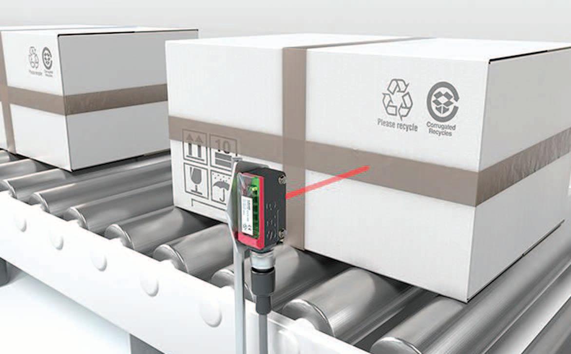
The larger the number of sensors to be mounted on a conveyor line is, the more important the cost effectiveness aspect becomes with respect to the time and cost of mounting and commissioning.
The intelligent and simple fastening concept with two convenient M3 metal threads facilitates fast mounting for the user.
The small and compact housing design also makes installation in small spaces easier.
Depending on your individual preference or local installation situation, various connection types are available, e.g., with M8 connector, cable, or pigtail connector.
Fast and simple commissioning and alignment
360° indicator LEDs ensure easy installation and a clearly discernible status display. Simple alignment of the sensor through the easily visible light spot results in an additional time saving and therefore in a reduction in costs for the user.
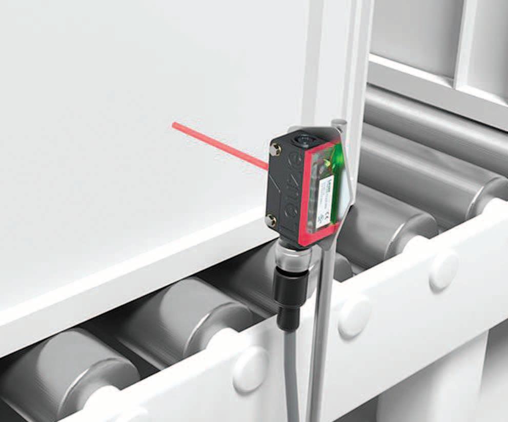
The new 5B series is also available as a model with potentiometer for better fine adjustment of the sensor. The sensor can thus be quickly and easily adapted to new application conditions. Moreover, the light/dark switching of the switching output can be performed in a tamperproof manner via the wiring.
Reliable detection even with depolarizing objects
In conveyor and storage systems, it is often the case that pallets, cardboard boxes and other containers are wrapped in film, which can be challenging for the sensor system. With the new 5B series, we offer optimized models especially for this area of application. These sensors guarantee safe switching even with shrink-wrapped or shiny objects.

Application
Presence control in intralogistics using retro-reflective photoelectric sensors

Requirement: In a logistics center, various containers and cardboard boxes are to be transported on roller conveyors that are positioned closely to each another. In addition, some cardboard boxes are shrink-wrapped in film. All objects must be reliably detected. During commissioning, the sensor must be fast and simple to install, align, and adjust. The light spot must be easy to see. Solution: With their compact, space-saving housing, the new 5B series sensors can be mounted directly on roller conveyors that are positioned closely to each other. The sensors are installed and securely mounted using convenient metal inserts with M3 thread. They are aligned quickly and easily using a homogeneous and clearly visible light spot as well as 360° indicator LEDs. Adjustment is user-friendly by means of a potentiometer. Performance optimized for the detection of shrink-wrapped and glossy objects ensures that they can be reliably detected.
Presence control in packaging systems using throughbeam photoelectric sensors

Requirement: At a food manufacturer's plant, potato chips are packed in primary packaging. The packages are then transported further on a conveyor line where they are to be reliably detected. The light spot must be visible. The sensor state should also be visible from a distance of 2 m.
Solution: The new sensor of the 5B series can also be mounted horizontally on the conveyor line, and the light spot is easy to see. Thanks to the bright 360° indicator LEDs, the sensor state is visible at all times, even at some distance away from the conveyor line. The advantage of the throughbeam photoelectric sensor is the very high function reserve. This ensures reliable detection even in very demanding environmental conditions, and it reduces the risk of system downtimes. Furthermore, the new 5B series has an optimized switching frequency of 900 Hz.
www.oboyle.ro