Download pdf Analog integrated circuits and simulation lab manual ecl331 1st edition v s jayaraj ful
Visit to download the full and correct content document: https://ebookmeta.com/product/analog-integrated-circuits-and-simulation-lab-manualecl331-1st-edition-v-s-jayaraj/
More products digital (pdf, epub, mobi) instant download maybe you interests ...
BY JAYARAJ V S ASSISTANT PROFESSOR DEPARTMENT OF ECE SREE BUDDHA COLLEGE OF ENGINEERING PATTOOR
Department of Electronics and Communication Engineering
Sree Buddha College of Engineering, Pattoor Vision
To nurture professionally competent and socially responsible Electronics and Communication Engineers
Mission
Provide knowledge, facilities and value-based education for developing competent Engineers
Promote industry-institute interaction, lifelong learning and research
Inculcate ethical and interpersonal skills to address the societal needs
Program Educational Objectives (PEOs)
The graduates will:
Acquire capability to analyze, formulate and solve problems in Electronics and Communication Engineering
Develop a quest for lifelong learning, research and entrepreneurship for professional development
Be motivated to address societal needs through sustainable and ethical practices
GENERAL RULES FOR PERSONAL SAFETY
1. Always wear tight shirt/lab coat, pants and shoes inside the lab.
2. REMOVE ALL METAL JEWELLERY since rings, wrist watches or bands, necklaces, etc. make excellent electrodes in the event of accidental contact with electric power sources.
3. DO NOT MAKE CIRCUIT CHANGES without turning off the power.
4. Make sure that equipment working on electrical power are grounded properly.
5. Avoid standing on metal surfaces or wet concrete. Keep your shoes dry.
6. Never handle electrical equipment with wet skin.
7. Hot soldering irons should be rested in its holder. Never leave a hot iron unattended.
8. Avoid use of loose clothing and hair near machines and avoid running around inside lab.
Preamble: This course aims to (i) familiarize students with the Analog Integrated Circuits and Design and implementation of application circuits using basic Analog Integrated Circuits (ii) familiarize students with simulation of basic Analog Integrated Circuits.
Prerequisite: ECL202 Analog Circuits and Simulation Lab
Course Outcomes: After the completion of the course the student will be able to
CO 1 Use data sheets of basic Analog Integrated Circuits and design and implement application circuits using Analog ICs.
CO 2 Design and simulate the application circuits with Analog Integrated Circuits using simulation tools.
CO 3 Function effectively as an individual and in a team to accomplish the given task.
Mapping of course outcomes with program outcomes
End Semester Examination Pattern: The following guidelines should be followed regarding award of marks
(a) Preliminary work : 15 Marks
(b) Implementing the work/Conducting the experiment : 10 Marks
(c) Performance, result and inference (usage of equipment and troubleshooting): 25 Marks
(d) Viva voce : 20 marks
(e) Record : 5 Marks
General instructions: End-semester practical examination is to be conducted immediatelyafter the second series test covering entire syllabus given below. Evaluation is to be conducted under the equal responsibility of both the internal and external examiners. The number of candidates evaluated per day should not exceed 20. Students shall be allowed for the examination only on submitting the duly certified record. The external examiner shall endorse the record.
LIST OF EXPERIMENTS
I. Fundamentals of operational amplifiers and basic circuits [Minimum seven experiments are to be done]
1. Familiarization of Operational amplifiers - Inverting and Non inverting amplifiers, frequency response, Adder, Integrator, Comparators.
2. Measurement of Op-Amp parameters.
3. Difference Amplifier and Instrumentation amplifier.
4. Schmitt trigger circuit using Op–Amps.
5. Astable and Monostable multivibrator using Op-Amps.
6. Wien bridge oscillator using Op-Amp - without & with amplitude stabilization.
7. RC Phase shift Oscillator.
8. Active second order filters using Op-Amp (LPF, HPF, BPF and BSF).
9. Precision rectifiers using Op-Amp.
II. Application circuits of 555 Timer/565 PLL/ Regulator (IC 723) ICs [ Minimum three experiments are to be done]
1. Astable and Monostable multivibrator using Timer IC NE555
2. DC power supply using IC 723: Low voltage and high voltage configurations, Short circuit and Fold-back protection.
3. D/A Converters - R-2R ladder circuit.
III. Simulation experiments [The experiments shall be conducted using SPICE]
1. Simulation of any three circuits from Experiments 3, 5, 7, 8, 9and 11 of section I
2. Simulation of Experiments 3 from section II
I. Fundamentals of operational amplifiers and basic circuits
EXPERIMENTS-I-1
Familiarization of Operational amplifiers - Inverting and Non inverting amplifiers, frequency response, Adder, Integrator, Comparators.
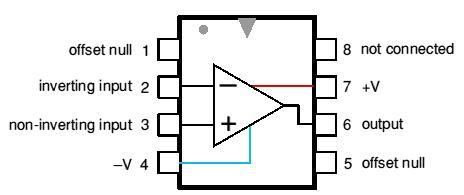
AIM: To familiarize with μC741C operational amplifier IC and its electrical characteristics.
1) FAMILIARIZATION OF OPERATIONAL AMPLIFIERS
AIM: To familiarize with μC741C operational amplifier IC and its electrical characteristics.
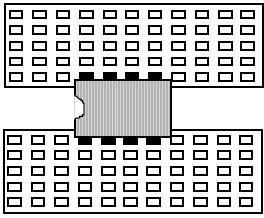
741 op amp IC
Insert the ICs (carefully to avoid bending their leads) into the wider strips, as shown above: Plug an op-amp into the breadboard so that it straddles the gap between the top and bottom sections of the socket strip.
If you have wired the power buses as suggested above, Pin 1 should be to the left.
Warning:
Do not try to unplug the op-amp with your thumb and forefinger. Use the IC puller or tip of a pen for unplugging.
PARAMETER IDEAL GENERAL PURPOSE 741 OPAMP
Voltage Gain, A ∝ 1 x 10⁵
Output Impedance, Ro 0 75Ω
Input Resistance, Rin ∝ 2MΩ
Offset Current, Iio 0 20nA
Offset Voltage, Vio 0 2mV
Bandwidth, BW ∝ 1MHz
Slew rate, SR ∝ 0.5 V/µs
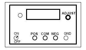
Throughout this experiment use the external dual DC Power Supply Unit shown in figure below.
Use the dual trace oscilloscope to observe the shape and to measure the amplitude of the input and output waveforms.
Connecting an Op-Amp to Power Supply Unit:
Turn the Power Supply ON. Adjust the voltage of the Power Supply to 15V. This will set both positive and negative power sources respectively to +15V and –15V.
Turn the Power Supply OFF before connecting to the circuits.
Connect the POS terminal of the Power Supply to the Vcc+ of your circuit. Connect the NEG terminal of the Power Supply to the Vcc- of your circuit. Connect the COM terminal of the Power Supply to the ground of your circuit.
Front panel of power supply unit
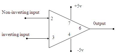
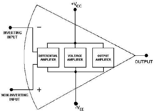
Symbol Of Op-Amp
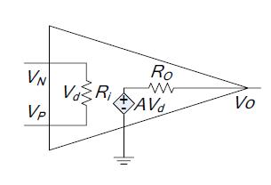
A Equivalent Circuit Of An Op-Amp
A Internal block diagram of Op-Amp:
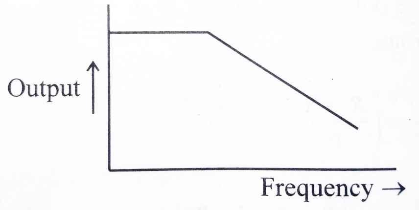
2) FREQUENCY RESPONSE OF AN OP-AMP
In an Op-Amp Bandwidth, frequency response & gain bandwidth product are key parameters for any circuit. Typically, Op-Amps are used for comparatively low frequency circuit but with the performance of these chips is improving all the time, much higher bandwidth Op-Amps are available.
The frequency response of a typical Op-Amp chip will often start to fall at a very low frequency when operated in its open loop mode. The point at which the frequency starts to roll off is known as break point.
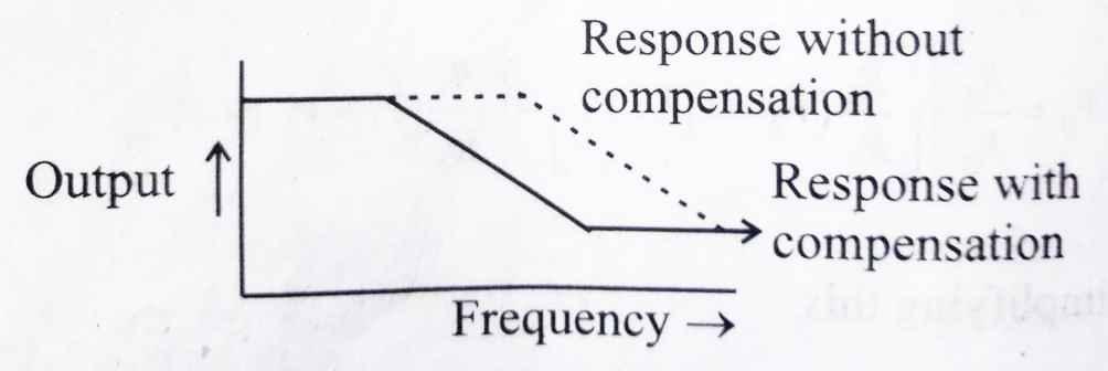
Frequency compensation added in most of OP-AMP chips. It is introduced to ensure that they remain stable& do not produce unwanted high frequency spurious oscillations.
The frequency response of open loop OP-AMP is shown above
(Op-Amp frequency Response With & Without Frequency Compensation)
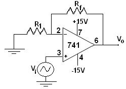
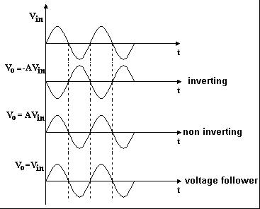
3) INVERTING, NON-INVERTING AMPLIFIER AND VOLTAGE FOLLOWER
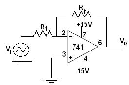
Inverting Operational Amplifier
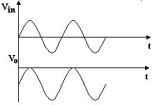
In the inverting operational amplifier circuit, the signal is applied at the inverting input and the non-inverting input is connected to the ground. In this type of amplifier, the output is 180⁰ out of phase to the input, i.e., when positive signal is applied to circuit, the output of the circuit will be negative.
Circuit Diagram
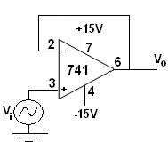
Non-Inverting Operational Amplifier
When the signal is applied at the non-inverting input, the resulting circuit is known as NonInverting Op-Amp. In this amplifier the output is exactly in phase with the input i.e., when a positive voltage is applied to the circuit, the output will also be positive.
Circuit Diagram
Voltage Follower
A voltage follower (also known as a buffer amplifier, unity-gain amplifier, or isolation amplifier) is an op-amp circuit whose output voltage is equal to the input voltage (it “follows” the input voltage). Hence a voltage follower op-amp does not amplify the input signal and has a voltage gain of 1.
The voltage follower provides no attenuation or amplification—only buffering.
Circuit Diagram
Model graph:
DESIGN:
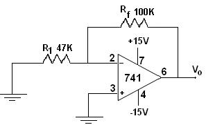
I Inverting Amplifier
A = -Rf/R1 (Voltage gain)
Take A =5
Rf = 5R1
Choose Rf = 10kΩ, R1=2kΩ
II Non-Inverting Amplifier
A = 1+ Rf/R1
Take A = 2
Rf = R1
Choose Rf = 10kΩ, R1=10kΩ
PROCEDURE:
I Inverting Amplifier
1. Construct the inverting amplifier circuit shown in figure.
2. Manually trace the circuit to check the correctness of physical connection.
3. Calibrate the CRO.
4. Apply 1V amplitude, 1 kHz sinusoidal input signal to the amplifier.
5. Observe the input and output waveforms simultaneously on CRO.
6. Compare the phase of input and output signals.
7. Record the output waveform amplitude.
8. Increase the amplitude of the input until distortion occurs at the output.
9. Record the corresponding output amplitudes and plot a graph of the output amplitude vs the input amplitude.
II Non-Inverting Amplifier
1. Construct the non-inverting amplifier as shown in the figure.
2. Apply 1V amplitude, 1 kHz sinusoidal input signal to the amplifier.
3. Observe Vin and Vo at the same time on the CRO.
4. Verify whether the output is in phase with the input.
5. Note down the output voltage by varying the frequency of the input signal.
6. Draw its frequency response characteristics.
III Voltage Follower
1. Wire up the voltage follower circuit.
2. Apply a sine wave of frequency 10 KHz, with amplitude of approximately 1.0 V to the circuit.
3. Observe Vin and Vo at the same time on the CRO.
4. Confirm that input and output amplitudes are equal.
OBSERVATION:
1) Inverting Amplifier
Vi = 1V
f (Hz) Vo(V) Av(dB)
2) Non inverting Amplifier
Vi = 1V
f (Hz) Vo(V) Av(dB)
3) Voltage follower
f (Hz) Vin(V) Vo(V)
4) ADDER, INTEGRATOR, COMPARATORS.
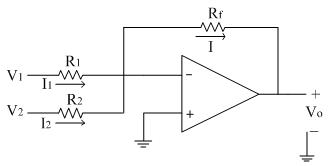
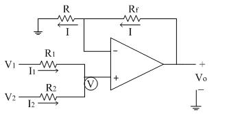
a) Adder: Adders are of two types Inverting and Non-Inverting type.
i)Inverting adder:
The input signals to be added are applied to the inverting input terminal of op-amp. The following figure shows the inverting adder using op-amp with two inputs V1 and V2.
Here Vo is output and is defined by the formula
ii) Non-inverting adder:
The input signals to be added are applied to the non-inverting input terminal of op-amp. The following figure shows the non- inverting adder using op-amp with two inputs V1 and V2.
Here Vo is output and is defined by the formula
�������� =�������� = ����
OBSERVATION:
1)Inverting Adder
2) Non inverting Adder
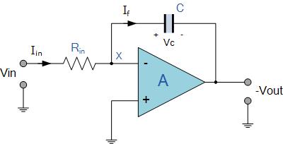
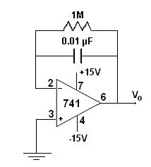
b) Integrator:
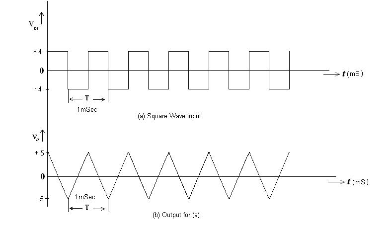
The Op-amp Integrator is an operational amplifier circuit that performs the mathematical operation of Integration, that is we can cause the output to respond to changes in the input voltage over time as the op-amp integrator produces an output voltage which is proportional to the integral of the input voltage.
CIRCUIT DIAGRAM:
Model graph:
Design:
Given f =1 KHz
So, T = 1/f = 1ms
Design equation is T = 2πRinC
Let C = 0.01μF
Then Rin = 15KΩ
c) Comparators:
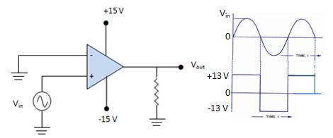
The Op-amp comparator compares one analogue voltage level with another analogue voltage level, or some preset reference voltage, VREF and produces an output signal based on this voltage comparison. In other words, the op-amp voltage comparator compares the magnitudes of two voltage inputs and determines which is the largest of the two. There are three major types of comparators which will be discussed.
i) Zero crossing Detector:
When one input of a comparator is connected to ground, it is known as zero crossing detector because the output changes when the input crosses 0 V. The zero-crossing circuit is shown in figure below with its input and output wave forms.
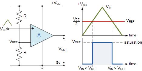
ii) Positive Voltage Comparator:
The basic configuration for the positive voltage comparator, also known as a non-inverting comparator circuit detects when the input signal, VIN is ABOVE or more positive than the reference voltage, VREF producing an output at VOUT which is HIGH as shown.
Non-inverting Comparator Circuit
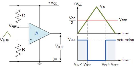
iii) Negative Voltage Comparator
The basic configuration for the negative voltage comparator, also known as an inverting comparator circuit detects when the input signal, VIN is BELOW or more negative than the reference voltage, VREF producing an output at VOUT which is HIGH as shown.
Inverting Comparator Circuit
RESULT:
EXPERIMENT-I-2
Measurement of Op-Amp parameters.
AIM: To measure the following parameters of an Op-amp
1. Input offset voltage
2. Input bias current
3. Input offset current
4. CMRR
5. Slew rate
The characteristics of an ideal op-amp are as follows:
(viii) Characteristics do not drift with temperature
1) Input offset voltage: Input offset voltage is the differential input voltage that exists between the inverting and non-inverting input terminals of an op-amp. In other words, this can be defined as the voltage that is to be applied between the two input terminals for making the output voltage zero.
2) Input bias current: The input bias current is the average of the currents that flow into the inverting and non-inverting input terminals of an op-amp.
3) Input offset current: The input transistors of an Op-Amp cannot be made identical, and there always exists a small difference between the bias currents IB1 and IB2. The difference in magnitude between IB1 and IB2 is called input offset current.
4) CMRR: It is is the ratio of the common-mode gain to differential-mode gain or in other words the ability of an Op-Amp to reject common mode signals.
PROCEDURE:
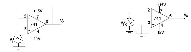
1) Input Offset Voltage
1. Connect the circuit as shown in figure.
2. Manually trace the circuit to check the correctness of physical connection.
3. Calibrate the CRO.
4. Measure the output voltage and record the result in the table given.
5. Calculate the input offset voltage using the expression ()if fo io RR RV V + = where Vo= output voltage and Vio=input offset voltage.
6. Compare this value with the theoretical value.
2) Input Bias Current
1. Set up the circuit as shown.
2. Measure the output voltage and record it in the table given.
3. Calculate IB1 and IB2 using the expressions Vo = IB1R. and Vo = IB2R.
4. The input bias current can be calculated as I = (IB1+IB2)/2.
5. Compare this value with the theoretical value.
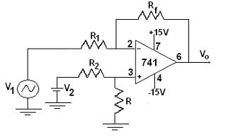
3) Input Offset Current
1. Reconnect the circuit as shown.
2. Follow the above steps 2 and 3.
3. The input offset current can be calculated as I = IB1-IB2.
4. Compare this value with the theoretical value.
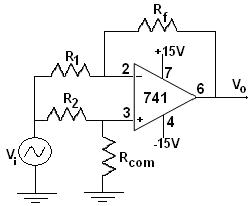
4) CMRR
1. Set up the circuit for finding CMRR.
2. Apply an ac signal of 0.5V as input and measure Vo.
3. Calculate the common mode gain, Ac=Vo/Vi and differential mode gain, Ad=Rf/R1.
4. Then find CMRR as CMRR=Ad/Ac.
5. Express CMRR in dB using the expression 20 log (CMRR).
6. Choose Rf, Rcom =100KΩ and R1, R2=100Ω
5) Slew Rate
1. Connect the circuit as illustrated in figure.
2. Apply a 1 KHz, 1 Vp-p sinusoidal signal as input.
3. Vary the input frequency and observe the output voltage.
4. Note down the frequency at which the output gets disturbed.
5. Record the values in the table.
6. Measure the slew rate using the expression, SR= 6 10 2 fVmπ V/ µs.
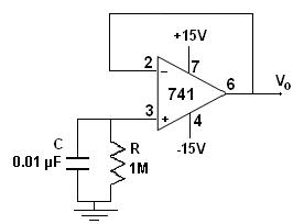
Slew rate can also be measured using a zero-crossing detector. For that 1. Feed a square wave as input.
2. Increase the frequency until rising and trailing edges of the output square wave becomes slanting or the output voltage from the square wave looks like a triangular wave.
3. Slew rate can be obtained from the slope of trailing or leading edge as SR= t Vo ∆ ∆ .
CIRCUIT DIAGRAM
Input Offset Voltage
Bias current Ib2 CMRR
Slew Rate
Slew Rate
OBSERVATION:
1. Input Offset Voltage
Theoretical Value
Actual Value
2. Input bias current
Theoretical Value
Actual Value
3. Input offset current
Theoretical Value
Actual Value
4. CMRR
Theoretical Value
Actual Value
5. Slew Rate
Theoretical Value
Actual Value
CALCULATIONS:
RESULT:
EXPERIMENT-I-3
Difference Amplifier and Instrumentation amplifier
AIM 1: To design and set up the Difference Amplifier circuits
DIFFERENCE AMPLIFIERS:
A difference amplifier is a special purpose amplifier designed to measure differential signals, otherwise known as a subtractor. A key feature of a difference amplifier is its ability to remove unwanted common mode signals, known as common mode rejection (CMR). Unlike most types of amplifiers, difference amplifiers are typically able to measure voltages beyond the supply rails, and are used in applications where large dc or ac common-mode voltages are present. They are ideal for current and voltage monitoring.
Circuit Diagram:
Model Graph:
DESIGN:
Assume 1R = 2R and f R = R
Vo= ()12 1 VV R R f
PROCEDURE:
1. Set up a difference amplifier circuit as shown in figure.
2. With Vi adjusted to produce a 1 V peak sine wave at 1 kHz, observe the output voltage VO (and Vi to note the phase relationship) on an oscilloscope.
3. Sketch the output voltage waveform. Be sure to note the dc level in the output.
4. Interchange the 5 V dc power supply and the 1 V peak signal generator. Repeat procedure step 3.
5. Measure Vout for three or four different values of V1 and V2, and verify that )(21VVV o −=
CALCULATIONS:
OBSERVATION:
RESULT:
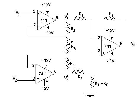
AIM 2: To design and set up an instrumentation amplifier using three op-amps to obtain an overall gain of 900 given input signal amplitude is 15mV and to measure the CMRR.
INSTRUMENTATION AMPLIFIERS:
Instrumentation Amplifiers are basically used to amplify small differential signals. Instrumentation Amplifier provides the most important function of Common-Mode Rejection (CMR). It cancels out any signals that have the same potential on both the inputs. The signals that have a potential difference between the inputs get amplified.
An Instrumentation Amplifier (In-Amp) is used for low-frequency signals (≪1 MHz) to provide a large amount of Gain. It amplifies the input signal rejecting Common-Mode Noise that is present in the input signal.
Circuit Diagram:
DESIGN:
Let Av1= Av2= 3
Here Av1= 5 542 R RR AVdiff + =
Ω= kR14
5 R =potk Ω 1
Choose
2 Av =3 And Rf = 3��������
R1=R2=1kΩ
Rf=R3=3KΩ
2 1 Av Rf R = =1kΩ
PROCEDURE:
1) Verify whether the op-amps are in good condition.
2) Manually trace the circuit to check the correctness of physical connection.
3) Calibrate the CRO.
4) Set up V1=0.5V dc and V2=0.4V dc and measure output voltage on CRO keeping R5 in maximum position
5) Repeat the step 4 by keeping R5 in minimum position. Note down the increase in gain. This is the difference mode gain, Ad.
d V V A =
6) Feed V1=V2=0.5V and observe the gain keeping R5 in minimum position. This is the common mode gain Ac ic oc c V V A =
7) Calculate CMRR from the relation CMRR=20 log (Ad/Ac).
OBSERVATION: Common Mode Gain
CALCULATION: CMRR =
RESULT:
EXPERIMENT-I-4
Schmitt Trigger circuit using Op–Amps
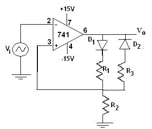
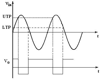
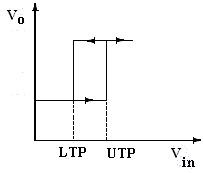
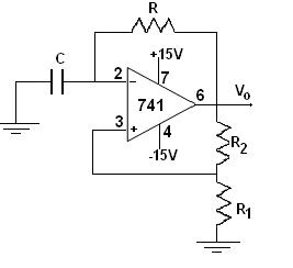
AIM: To design and set up an inverting Schmitt Trigger using op-amp for an LTP = 2V and a UTP = 3V.
SCHMITT TRIGGER:
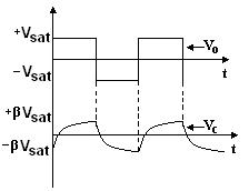
Schmitt Trigger was invented by Otto Schmitt in early 1930’s. It is an electronic circuit that adds hysteresis to the input-output transition threshold with the help of positive feedback. Hysteresis here means it provides two different threshold voltage levels for rising and falling edge.
Essentially, a Schmitt Trigger is a Bi-stable Multivibrator and its output remains in either of the stable states indefinitely. For the output to change from one stable state to other, the input signal must change (or trigger) appropriately.
This Bistable operation of the Schmitt Trigger requires an amplifier with positive feedback (or regenerative feedback) with a loop gain greater than one. Hence, Schmitt Trigger is also known as Regenerative Comparator.
Note: A square wave generator.
CIRCUIT DIAGRAM
MODEL GRAPH
DESIGN:
Assume o V = Vcc-1V = ± 14v
2)( RR RVVFo + ×−
UTP = 21
2)( RR RVVFo + ×−
LTP= 23
Here 2 2 2 I V R R =
Where 2 VR is either UTP or LTP 2 I is assumed as 50µ
PROCEDURE:
Hysteresis curve
1. Make connections according to the circuit diagram.
2. Manually trace the circuit to check the correctness of physical connection.
3. Calibrate the CRO.
4. Adjust the signal generator to produce a 5Vp-p, 1 KHz sine wave as the input.
5. Verify the input and output simultaneously on CRO.
6. Measure and record the output amplitude and frequency.
7. Observe the hysteresis curve on CRO by keeping the time/div knob of CRO in xy mode and feed Vin to the x-channel and Vo to the y-channel.
CALCULATIONS:
RESULT:
EXPERIMENT-I-5
Astable and Monostable multivibrator using Op-Amps
AIM 1: To design and set up an astable multivibrator circuit using op amp whose frequency of operation = 1 KHz.
ASTABLE MULTIVIBRATOR:
An astable multivibrator is a type of multivibrator that does not require a triggering pulse thus, sometimes known as a free-running multivibrator. It necessarily provides square wave as its output.
Astable multivibrator is called so because both the states present here are unstable i.e., quasistable. Here, the successive transition is made from one quasi-state to other after some predecided time interval.
CIRCUIT DIAGRAM
MODEL GRAPH
PROCEDURE:
1. Give the circuit connections as per the circuit diagram.
2. Manually trace the circuit to check the correctness of physical connection.
3. Calibrate the CRO.
4. Observe the output from CRO.
5. Sketch the capacitor and output waveforms.
6. Measure the time period of the output voltage waveform and compare it with the designed value.
7. Repeat the procedure for different duty cycles.
DESIGN:
Use 116.12RR = for equation RC f o 2 1 = to be used