
Discover 2022 Scientific Report


The Electronic Materials Platform of Reference Integrated Capabilities Enable Unique Co-optimized Solutions Successful Combined Solutions Our Customers Are Using Today Formulated cleans for 3D NAND Solid precursors for logic and memory Liquid packaging for advanced photoresist Purged wafer environments for improved defect control Reticle pods for EUV mask integrity Advanced materials and safegasdelivery AMH Advanced Materials Handling Protecting wafers and reticles from contamination or damage and delivering clean chemistries SCEM Specialty Che micals andEngineeredMaterials APS Advanced Planarization Solutions End-to-end CMP solutions Device Performance and Yield Microcontamination Control Enabling technologies MC fordefect reduction and yieldimprovement Clean chemical delivery and sensing solutions matched to emerging chemistries
Entegris, Inc. | 2022 Scientific Report 1 Table of Contents LETTER — Welcome to Our 2022 Scientific Report 2 ARTICLES — Science at the Interface 5 Introduction to Surfaces and Interfaces Embedding Computational Chemistry in Material Development 13 Applications of Molecular Dynamics on Formulation Design for Complex HAR 3D Nanostructures Modifying Polymer Surfaces for Contamination Control 23 Challenges and Opportunities for Improved Device Yield Semiconductor Materials Supply Chain for 2030 29 Hydrogen Gas for Semiconductors and Clean Energy ............................ 35 New Surface Chemistry Challenges
Welcome to Our 2022 Scientific Report

If you’re reading this on a touchscreen-enabled device, you are actively participating in surface science, based on the interaction of your finger and the screen. A voltage is applied to a thin, conductive coating creating an electrostatic field. When you touch the screen to zoom in or scroll down, the charge is transferred to your finger, and sensors identify and measure where a change in charge has occurred. The proximity of your finger to the screen matters because it is the interaction at the surface that gives you the ability to scroll down and read further.
Scientists across the world have studied the materials that can make these conductive layers while also understanding how the interfaces between the conductive layer, the protective covering, and your finger interact. Similarly, scientists at Entegris routinely study solid-solid interactions, gas-solid interactions, liquid-solid interactions, and all the combinations in between to best understand how materials used in a variety of high-tech industries interact. We believe materials science is most interesting and challenging at surfaces.
Entegris, Inc. | 2022 Scientific Report 2
This year’s scientific report focuses on surface science, the study of chemistry and physics that happens at interfaces.
In last year’s report, we highlighted the ways in which Entegris enables the semiconductor and pharmaceutical industries, concentrating on our innovations that deliver the products to enable our digital world. This year, we’re focusing further on how surface science enables those innovations. We start the report by describing the complicated process steps and characterization techniques that are used to precisely deposit, remove, pattern, and transform the surfaces that create an integrated circuit. Within that story, we describe how Entegris’ research and development enables advanced logic and memory device manufacturing and enhances specific unit processes.
At the heart of this innovation is our unrelenting commitment to collaborate closely with our customers. They inspire and motivate us to push the limits of today’s technology and deliver breakthrough solutions for the future. To facilitate this collaboration, we engage with our customers at technology centers located strategically throughout our global operations in close proximity to their manufacturing sites. To further expand our opportunities to collaborate successfully with our customers and create innovative solutions that address the CMP challenges they face, CMC Materials became part of Entegris in July 2022. This transaction further expands Entegris’ R&D footprint and has created an even larger community of innovative scientists and engineers ready to engage and serve our customers.
These are unprecedented times, especially for our industry. Between 2010 and 2020, the semiconductor industry grew from $250B to $500B. Between now and 2030, the industry is anticipated to double again to $1T. The demands on the materials supply chain to sustain such a level of growth are staggering, and Entegris’ innovative mindset will ensure that we play a key role in this growth.
In addition to focusing on enabling new technologies with increasing volumes of materials, we must also consider how we will do so in a sustainable manner. This year’s report describes how Entegris will address the growing demand for semiconductors while also ensuring that our innovations are a force for positive change that not only meets the needs of our customers but also improves the lives of our teams and the communities where we work.
Sincerely,
James A. O’Neill, Ph.D. Senior Vice President and Chief Technology Officer

Entegris, Inc. | 2022 Scientific Report 3

SCIENCE AT THE INTERFACE Introduction
to Surfaces and Interfaces
 Authors: Jennifer Braggin
Thomas Phely-Bobin, Ph.D.
Authors: Jennifer Braggin
Thomas Phely-Bobin, Ph.D.
Surface science forms the scientific basis for everything that Entegris does, whether it’s functionalizing the surface of polymer membranes for enhanced liquid filtration, formulating new liquid chemistries for better surface cleanliness, developing etch chemistries or precursor molecules to engineer materials on surfaces, or devising polishing slurry mixtures to control the morphology of critical films. Surface science specifically refers to the study of the chemical and physical processes that occur at the interface between two solids or between a solid and either a liquid or a gas. The presence of such an interface influences the thermodynamic parameters of a system and controls processes like crystal growth, adsorption, and diffusion, as well as chemical reaction events such as etching, deposition, and corrosion.
The field of surface chemistry traces its roots to the early 1900s with Fritz Haber’s discovery of a heterogeneous catalysis process for the synthesis of ammonia. This development revolutionized the production of synthetic fertilizers used throughout the agricultural industry. Irving Langmuir also contributed significantly to the fundamental understanding of surface phenomena, and the Langmuir equation is used to describe the process of monolayer adsorption. Over the next 50 years, significant progress was achieved in characterizing metal and insulating surfaces to better describe the interaction between adsorbed molecules and the solid material. This focus led to advancements in high vacuum technology as well as analytical techniques such as low-energy electron diffraction (LEED), time-of-flight secondary ion mass spectroscopy (TOF-SIMS), Auger electron spectroscopy (AES), and X-ray photoelectron spectroscopy (XPS) (Figure 1).
Entegris, Inc. | 2022 Scientific Report 5
An understanding of the chemistry that occurs on solid surfaces is critical to the semiconductor industry where engineered materials impart function or structure to the surface – such as that needed to build a transistor device on a silicon wafer. Today’s most advanced chips contain tens of billions of transistors, each with critical structures of roughly 5 nm. Such miniaturization requires the uniform deposition and selective removal of material at atomic scale dimensions. This is an extraordinary level of process control that can only be achieved through a precise understanding and skilled manipulation of fundamental chemical processes on the surface. Surface phenomena that must be considered for depositing thin films at the solid-gas interface include selective adsorption and thermal decomposition of precursor molecules on materials of differing composition (metal vs. insulator). For the selective etching of a single film in a complex material stack, phenomena such as surface diffusion, selective reaction on targeted surfaces, and desorption are important.
At the solid-liquid interface, electrochemistry controls many of the phenomena that occur on the surface. Electrochemistry is a thermodynamically favorable process that occurs in response to an electrical potential. This potential can arise from differences in the half-cell reactions of different materials in the system – for example, two different metals on a surface in a wet processing environment. The simplest type of electrochemistry is corrosion that
results from the two half-cell reactions of reduction and oxidation (redox). The corrosion process occurs as a result of the formation of a galvanic cell where the metal acts as the anode. Understanding the electrochemistry of a system also allows the process to be used to its advantage, such as in the deposition of critical films for semiconductor applications. In fact, for the last 25 years, electroplating of copper has been the preferred method for achieving the thin conductive wires used to interconnect the billions of transistor devices on a chip. Advances in electroplating chemistry have enabled precise control of the deposition process to achieve high quality, conductive wires tens of nanometers in dimension.
While the focus is often on surface science for semiconductors, there are many more surfaces involved in other industries that also require attention. To deliver chemistries across industries, there are many surface interactions. The chemistries are handled in drums and canisters and delivered to wafer surfaces through miles of tubing and hundreds of filters. The surfaces in these components also require special consideration as the interaction of the chemistry with these surfaces can create adverse reactions that generate contamination. Contaminants like organics, metallics, particles, and moisture can all have adverse impacts on sensitive processes. Therefore, it is also important to understand the surface interactions in these components to ensure the purity of the entire system.

Entegris, Inc. | 2022 Scientific Report 6
Figure 1. The development of surface science along the S-curve drives new capabilities that build upon one another to increase our understanding of science at interfaces and drive new semiconductor technologies.1
Time Field Maturity
Structure and electron structure of clean metal surfaces and simple adsorbates; vibrations; phase transitions
CHANGING THE SURFACE
Semiconductor manufacturing, at its core, is a series of controlled additive and subtractive steps (Figure 2). Many of the steps are repeated over 20-30 times, and all are designed to create a very precise surface. Entegris supports innovation in each of these unit process steps to design and deliver high-purity materials that can create these surfaces.
The development of materials that can be highly conformal in HAR structures is quite challenging. One important consideration is controlling the surface termination of deposited films. Differences in the surface terminations between different exposed materials allows deposition to be controlled to affect some, but not all of the exposed surfaces.3 Selective deposition techniques, like atomic layer deposition (ALD), require specific materials design to achieve the required film properties and also enable ease of use. ALD is a technique that increases in use as more HAR structures are designed. It is different from traditional deposition steps because deposition materials are sequentially deposited on the surface a few atomic layers at a time. Through repeated exposures to different precursor materials, a highly conformal layer is grown. Precursor materials used in this process must be specifically designed to address the end-state of the surface being created.
Once materials are deposited, they must be patterned before they are etched. Patterning materials, in the form of photoresists and other photochemicals, require precise design and delivery to ensure an accurate pattern transfer. As extreme ultraviolet (EUV) lithography is adopted as a high-volume manufacturing process, new materials are being introduced to increase resolution and speed while decreasing variability.
ETCH
DEPOSITION
—
Insulators, conductors, and barrier materials are all deposited onto the surface of the wafer to build transistors. Significant innovations in materials design are required to enable advanced 3D device architectures like fin field effect FinFETs, gate-all-around (GAA) transistors, and 3D NAND memory devices, and to boost performance and reduce power requirements.
What makes these advanced devices unique is that they often require the creation of high aspect ratio (HAR) structures that, once created, require additional layers of deposition. Therefore, the ability to deposit highly conformal, thin layers is of utmost importance.
Etching has become one of the most difficult and important unit processes as both logic and memory devices move into the third dimension. Once HAR structures are patterned, they must be etched to transfer the pattern into the underlying materials. This creates a significant etch challenge, as these HAR structures are quite deep and narrow, making it difficult to transport the etch and subsequent cleaning chemistries to where they are needed to carry out the process. Even more challenging is the 3D aspect of some patterns, such as those formed when making 3D NAND. Not only are the structures deep and narrow, but there are horizontal areas out of the line of sight from the top of the wafer that also need to be etched and cleaned. These design changes dramatically increase the surface area to be etched and cleaned, and understanding the reaction at these surfaces is critical to efficiently design chemistries that achieve process and cycle time performance expectations in the fab.
Entegris, Inc. | 2022 Scientific Report 7
Figure 2. Semiconductor processing steps.2
Deposition precursor materials must be specifically designed to address the end-state of the surface being created.
—
20 – 30
Ion
Strip
Metrology Deposition Etch
Front-end Processing Certain steps repeated
times
Implant CMP
/ Clean
Photoresist Lithography
Collecting empirical data alone is no longer efficient or effective, so scientists worldwide are using new digital tools to understand these interactions, including density functional theory (DFT) and molecular dynamics (MD). More information about these techniques, their results, and their applications in materials designs at interfaces is described in Embedding Computational Chemistry in Material Development
PLANARIZATION
A number of processes typically found in the semiconductor industry involve chemistry that occurs on surfaces that are in motion relative to each other. The science that describes this field is known as tribology, and it is directly applicable to understanding chemical mechanical planarization (CMP) and brush cleaning of wafers (post-CMP cleaning). Chemical mechanical planarization is a process in which a wafer surface is smoothed and planarized through the combined action of chemical and abrasive forces. CMP was a radical idea when it was first introduced into highvolume manufacturing at the 0.35 µm node, creating a new level of complexity in the process. The slurry materials introduced had to be designed to selectively polish the different film features with high precision, and then those materials had to be reliably cleaned and removed from the surface after the process was complete.4 The subsequent brush cleaning process uses a chemically active formulation to remove slurry residue and polish debris remaining on the surface to eliminate any negative impact on succeeding fabrication steps. In this case, both the electrochemistry and the hydrodynamics of the system must be controlled to achieve clean and defect-free wafers.
Typically, the electrochemistry of the system is controlled by additives in the cleaning formulation, and tribology is controlled by the properties of the formulation in addition to the spin speed of the brush and the rotation of the wafer under it. Abrasive removal of material in CMP is controlled by engineered nanoparticles that are an integral component of the polishing slurry. In advanced slurries, the surface of the nanoparticle can be chemically treated to enable specific functionality such as preferential adhesion to one type of surface over another – viz. metal vs. dielectric. An important factor in this exercise is the Zeta potential, which is the electric potential at the
solid-liquid interface. When applied to nanoparticles in solution, the Zeta potential quantifies the tendency of the particle to adhere to a surface – that is, lending a desirable characteristic of enabling preferential polishing of a target material or an undesirable quality of making residual particles more difficult to remove during the cleaning process. Typically, Zeta potential can be controlled by engineering the chemical composition of the formulation, making it easier to detach the particles from the surface.
MODIFYING THE SURFACES OF COMPONENTS THAT ENABLE ADVANCED TECHNOLOGIES
Polymeric materials are an intrinsic part of the semiconductor manufacturing ecosystem. Tubing, canisters, drums, valves, filters, fittings, purifiers, and other supplies are all part of the system that brings critical chemistries to critical surfaces. Maintaining a high-quality interface between chemistries and polymeric components is essential in contamination control to avoid defects on the wafer. The surface properties of this interface can be modified to
1. effectively capture contaminants from chemistries and
2. prevent undesirable interactions at the interface that could result in contamination being released into the chemical stream.
One way to capture contaminants from chemistries is to modify the surface of filter membranes. Membranes have two primary mechanisms by which they can capture contaminants – size exclusion and adsorption. Size exclusion relies on the size of the porous pathways being smaller than the contaminants of interest. However, as defects of interest reduce in size, it is not possible to reduce the pores infinitely, as that will result in a loss of flow for a given pressure drop. Instead, surface modification is leveraged to create surfaces that can adsorb contaminants.5 However, there is no single, universal modification that can adsorb the contaminants of interest without negatively impacting the chemistry of interest.6 Significant research is required to tailor surface modifications to the application of interest. To better understand the science and unique approaches to determine the right surface modifications, the article Modifying Polymer Surfaces for Contamination Control goes into more depth.
Entegris, Inc. | 2022 Scientific Report 8
—
Polymers aren’t the only materials modified to enable the delivery of chemistries in advanced technologies. Entegris has conducted significant research in gas and air purification, which rely on two phenomena, chemisorption and physisorption, to capture molecular contaminants. Gases are used in deposition, etching, and photolithography. Hydrogen, in particular, is a gas that is used as a chemical reducing agent, heat transfer material, stabilizer, and can increase the resistivity of certain deposited materials. Hydrogen is an important gas in EUV lithography where it is employed as a purge and clean gas in the EUV chamber and its source. This critical chemistry requires part-per-trillion (ppt) levels of purity to ensure that mirrors and optic surfaces do not degrade when molecular contaminants decompose in the chamber and at the source.7 Entegris has developed several technologies, including adsorber purifiers and palladium membrane purifiers, to meet these stringent requirements. Beyond semiconductor manufacturing, these particular technologies that rely on surface science to capture molecules are being explored for new industries.
CHARACTERIZING THE INTERFACE
The ability to characterize the state of a surface is critical to controlling the processes used to create the surface. In the semiconductor industry, metrology measurements are necessary in all the steps of developing and manufacturing high-yielding integrated circuits.8 The parameters being measured are critical dimension, film thickness, defectivity, physical properties, surface, and interface properties. The semiconductor industry faces many challenges, especially in high throughput metrology and contamination detection in the bulk material and at surfaces (Figure 3). Many new chemistries (liquid and gas), new materials, and new components are introduced that require high levels of contamination control to ensure acceptable yields. Contaminants in the bulk can often be transferred to the surface after processing either through bulk migration or insolubility in chemistries and gases resulting in defects on surfaces. Contaminants often result in defects that are either random or systematic. Random defects are caused by particles that adhere to the surface, organic residuals or metal ions, and complexes that are left on the wafer during processing. Systematic defects are usually caused by the variation of mask and exposure conditions that result in a specific recurring defect.
Wafer optical inspection is either done on bare or patterned wafers. Dark-field microscopy remains the metrology of choice for defect inspection on bare wafers. Because of increasingly complex three dimensional topography both in logic and memory designs, patterned wafer inspection is comprised of state-of-the-art microscopy and spectroscopy and is also supported by advanced modeling and intricate post processing data analysis.9 Efficient on-wafer detection is becoming critical for high throughput manufacturing.10 Common in-line defect inspection techniques such as critical-dimension (CD) scanning electron microscopy (CD-SEM), CD atomic force microscopy (CD-AFM), CD small angle X-ray scattering (CD-SAXS), e-beam metrology with e-beam review (EBR) and e-beam inspection (EBI) are routinely used during manufacturing.11
Off-line highly sensitive metrology tools are often used during process development to characterize contaminants, but a gap still exists between detection limits and contamination levels on surfaces. Stateof-the-art liquid particle counters can reliably detect 20 nm particles at low particle concentration.
However, leading edge on-wafer detection today is limited to 13–14 nm defects. Smaller and undetectable defects are still a threat to both semiconductor yield and reliability. There is a real gap in particle detection both in the bulk and on wafer below 10 nm. Moreover, the increasing number of layers in new semiconductor design makes the challenge even more relevant, having to simultaneously detect different contaminants (ex. organic, ions, metals, and particles) and doing it in a cost-effective, time-sensitive manner.
Entegris, Inc. | 2022 Scientific Report 9
Figure 3. Example of available technologies for measuring liquid contaminants and possible targets.12
2 UPW Chemicals 10 20 30 50 Particle Size (nm) 100 200 500 300 5 Particle Concentration (# particles/mL) 108 107 106 105 104 103 102 10 0 DLS
LPC 40 nm DI/Chem LPC 30 nm Chem LPC 20 nm DI/Chem DMA+CPC
DLS = dynamic light scattering LPC = liquid particle counting DMA+CPC = di erential mobility analyzer + condensation particle counter
The concept of hybrid metrology is used both in fabs and analytical laboratories during process development. The identification and quantification of surface contaminants often require multiple techniques. Scanning and transmission electron microscopy (SEM and TEM), atomic force microscopy (AFM), and X-ray diffraction (XRD) are common techniques to identify the physical structure of the surface contaminants. Sub 10 nm features are still very challenging for these laboratory techniques, and are therefore combined with chemical and/or elemental composition characterization techniques such as: Raman spectroscopy, Fourier-transform infrared spectroscopy (FTIR), Auger electron spectroscopy (AES), X-ray photoelectron spectroscopy (XPS), and X-ray fluorescence (XRF). Other common bulk characterization such as gas and liquid chromatography, inductively coupled plasma mass spectrometry (ICPMS), and ion chromatography, are also used to complement surface analysis. Surface metrology will remain a significant challenge to the semiconductor industry for years to come.
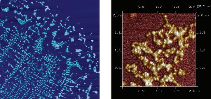

The Entegris laboratory network remains on the forefront of key contaminants detection. Our worldwide laboratories develop their own hybrid methodologies to identify surface contaminants. One such methodology is multi-modal imaging and analysis. This method analyzes a single sample using confocal laser 3D microscopy, AFM, SEM, electron dispersive spectroscopy (EDS), micro-Raman, microTIR, and nano-infrared (IR) spectroscopy. Alone, each of these techniques provide a single piece of information that can characterize contamination. When the data are combined, a holistic view of the contamination is revealed, providing the opportunity to identify root causes more quickly (Figures 4-5).13

SUMMARY —
Understanding the science at interfaces is the foundation of Entegris’ contributions to enabling advanced technologies in semiconductor manufacturing, green energy, and beyond. The ability to control processes that occur on surfaces with atomic scale precision and control is necessary to manufacture the high-performance structures required for autonomous vehicles, high-performance servers, or even your smart phone. Engineering materials at these vanishing dimensions requires a detailed understanding and precise control of the state and cleanliness of the interface where the chemical and physical processes of interest are occurring. A deep understanding of the processes that occur on such surfaces is instrumental to ensuring the integrity of a high-performance, pure material from the point where it is manufactured to the point where it is used in the process.
Entegris, Inc. | 2022 Scientific Report 10 SEM AFM CONFOCAL MICROSCOPE IMAGES Laser and Optical Height
Figure 4: A comparison of different imaging techniques. The sample is collected from a wet-etch process, SEM/EDS result shows the residue contains C, O, and Al.13
Figure 5. The residue collected from a deionized water sample. The right picture is a close-up image of AFM which shows aggregated particles.13
Fundamental advances in surface science continue to drive innovation that enables progress in a number of technical fields including semiconductor, life sciences, and energy science. It is equally important to recognize, however, the significance of all the surfaces that a material comes in contact with along an extended delivery path that may extend across several continents, over several months, and that represents today’s typical supply chain. In high-volume semiconductor manufacturing, high-throughput metrology remains a major challenge. Innovation is not only focused on “in-line” detection by combining most advanced microscopy techniques with modeling and complex post data analysis, but also in analytical laboratories to support contamination control of all materials throughout the supply chain.
Later in this report, we consider the supply chain for semiconductors, one such industry that requires the delivery of high-purity solutions to surfaces. The article Semiconductor Materials Supply Chain for 2030 highlights a scientific approach to estimate material needs for the changing supply landscape. As the global population increases and relies even more heavily on advanced technology to access information, there will be increasing challenges to our ability to innovate, design, and deliver materials to high-technology industries. It is therefore important to focus our efforts not only at the interfaces of materials, but also at the interfaces of communities and countries.
As a conscientious global citizen, Entegris can have a positive impact on new and emerging industries when we apply decades of learning from the demanding field of semiconductors to other areas with similar requirements. Green energy is a new industry that can be readily addressed by Entegris’ understanding of gas purification. More specifically, hydrogen, increasingly used for the generation and storage of energy, can be generated by many different methods. Each of the methods, however, will confront the challenge of purifying the gas, specifically removing moisture, and ensuring the integrity of the material as it is stored and transported for use. This is a problem that has long been addressed in the semiconductor industry, and the knowledge gained there can be adapted and used to address green energy, a topic which is explored in the final article: Hydrogen Gas for Semiconductors and Clean Energy: New Surface Chemistry Challenges.
When reflecting on the advances in surface science over the past century, it seems obvious that we’ve been able to use each discovery to drive the next.
If we reframe the challenges of the semiconductor manufacturing, supply chain disruptions, and green energy as if they were advances in surface science, we can begin to see how we can leverage learning in one area and apply it to another. We then identify unique interfaces that we didn’t know existed and create innovations there.
References
1 Repurposed and used with permission from: https://www. biolinscientific.com/blog/surface-science-how-it-all-began
2 Needham and Company, LLC, Looking forward to a C2H19 Recovery; Initiating coverage of semi cap industry, 2018.
3 H. Wang, B. Hendrix and T. Baum, Selective ALD of SiN using SiI4 and NH3: The effect of temperature, plasma treatment, and oxide underlayer, Journal of Vacuum Science and Technology A, vol. 38, no. 6, 2020.
4 G. Banerjee and R. Rhoades, Chemical Mechanical Planarization: Historical Review and Future Directions, ECS Transactions, vol. 13, no. 4, pp. 1 – 19, 2008.
5 J. Braggin, V. Goel and A. Wu, Expanding the lithographer’s toolkit to reduce variability: Filtration considerations, in SPIE Advanced Lithography, San Jose, CA, 2019.
6 J. Jaber, J. Hamzik, N. Filipancic, J. Brewster and A. Xia, Addressing metallic contaminants in the photochemical supply chain, in SPIE Advanced Lithography, San Jose, CA, 2020.
7 C. Landoni, M. Succi, C. Applegarth and S. R. Vogt, "EUV tools: Hydrogen gas purification and recovery strategies," in SPIE Advanced Lithography, San Jose, CA, 2015.
8 N. Orji, M. Badaroglu, B. Barnes, C. Beitia, B. Bunday, U. Celano, R. Kline, M. Neisser, Y. Obeng and A. Vladar, Metrology for the next generation of semiconductor devices, Nature Electronics, vol. 1, pp. 532–547, 2018.
9 S. Purandare, J. L. Zhu, R. J. Zhou, G. Popescu, A. Schwing and L. L. Goddard, Optical inspection of nanoscale structures using novel machine learning based synthetic image generation algorithm, Opt. Express, vol. 27, pp. 17743 – 17762, 2019.
10 J. Zhu, J. Liu, T. Xu, S. Yuan, Z. Zhang, H. Jiang, H. Gu, R. Zhou and S. Liu, Optical wafer defect inspection at the 10nm technology node and beyond, International Journal of Extreme Manufacturing, vol. 4, pp. 1 – 24, 2022.
11 E. Solecky, A. Vaid and B. Su, Metrology in the Semiconductor IC Industry, in Introduction to Metrology Applications in IC Manufacturing, 2015.
12 A. Rastegar, M. House and M. Samoya, Understanding UPW-induced particle defectivity in sub-10nm technology nodes, Albany, NY, 2014.
13 S. Liu and H. Zhang, Multi-Modal Imaging and Analysis for Microcontamination Source Identification, in International Conference on Frontiers of Characterization and Metrology for Nanoelectronics, Monterey, CA, 2019.
Entegris, Inc. | 2022 Scientific Report 11

EMBEDDING COMPUTATIONAL CHEMISTRY IN MATERIAL DEVELOPMENT
Applications of Molecular Dynamics on Formulation Design for Complex HAR
3D Nanostructures
 Authors: Albert Chen
Montray C. Leavy, Ph.D.
Authors: Albert Chen
Montray C. Leavy, Ph.D.
As the semiconductor industry continues to push the limits of performance, power, area, and cost (PPAC), the development and co-optimization of enabling new materials and device structures in semiconductor technologies become ever critical. In the past, we have experienced the migration of transistor structures from planar to FinFET devices, and we expect to enter another gate-all-around (GAA) epoch in the coming 3/2 nm tech nodes in a few years (Figure 1).
Entegris, Inc. | 2022 Scientific Report 13
New materials engineered at atomic dimensions enable new device architectures, new patterning schemes
Other novel structures such as forksheet and CFET are being developed to meet PPAC requirements for sub-2 nm nodes. In the evolution of these diversified structures, one shared trend is the increasing complexity and aspect ratio (AR) of 3D structures in logic, DRAM, and NAND flash structures. As designs continue to shrink, the storage cell must maintain a minimum charge. One approach to address this is to increase the height of the capacitor, resulting in a higher AR. To increase memory capacity in 3D NAND devices, the number of layers is increased, while the thickness of SiO/SiN pairs decreases, leading to an increase of AR in both vertical and lateral directions (Figure 2). The evolution to complex and high AR 3D structures has posed holistic challenges to almost all semiconductor process modules including:
• Etch
• Deposition
• Implant
• Cleans
This trend requires all industry members to address new phenomena in process development and control as device features continue to shrink.
HOW MODELING AND SIMULATION CAN BE USED TO AID IN CHEMISTRY DISCOVERY
—
In wet etch and clean processes, for example, when we apply wet chemistry to complex nanostructures, the chemical reactions tend to become more diffusion limited. As a result, the etch rate and cleaning performance reduces, and it takes longer to completely etch or clean a structure. Longer process time generally suggests longer manufacturing cycle time and higher costs. Longer process time also contributes to a shift in etch selectivity between different materials in a structure because longer process time may also lead to excessive loss of other materials. In addition, complex structures may also hinder the diffusion of etching byproducts, which consequently leads to issues in uniformity or process yields. Not only will nanostructures cause diffusion-related issues, but also directly change the nature of chemical reactions.
Entegris, Inc. | 2022 Scientific Report 14
Figure 2. High AR structures in DRAM and 3D NAND devices.
30 0 + 3D NAND DRAM Next Node: Shrink more
Moore’s Law Log (# transistors/$$) Year
Figure 1. Evolution of enabling material technologies and device architectures in semiconductor.
Doublepatterning FinFETdevice EUVlithography Nanowiredevice
“Easy”pitchscaling 2016 2018 2020 2022 2024 2026 2014 2012 2010 2008 2006 Atomic Level Processes New Metallurgies High-µ Channel Cobalt Contacts ALD Dielectrics High-k Metal Gate Strained Films Low-k BEOL Copper BEOL MP Films 65 nm 40 nm 28 nm 20 nm 14 nm 10 nm 7 nm 5 nm 3 nm 2 nm 1.x nm EUV light source Reticle Mirror Patterned wafer Mirror
EraofIncreasingMaterialsIntensity
In nanoscale 3D structures, the surface reactions become dominant owing to an increase in surfaceto-volume ratio. At the nanoscale, the movement of molecules in structures can be within the range of influence of some intermolecular forces and result in a shift of concentration or even depletion of chemical species within the nanostructures.1,2 A change of molecular arrangement has also been reported,3 as well as a change of chemical viscosity4 in nano-confined spaces. All such additional effects at the nanoscale inevitably will complicate the development, integration, and control of processes and related materials. In the front end of line (FEOL) where the critical dimensions are smallest and structures are most complex, some chemical suppliers are trying to improve the performance of conventional bulk chemistries at the nanoscale by incorporating functional additives such as surfactants. Therefore, it is expected that more formulated chemistries will be introduced in the FEOL in addition to the back end of line (BEOL) in future technology nodes.
No matter how formulations are designed or applied, the key challenge lies in the prediction and validation of their performance within complex nanostructures in targeted applications. Currently, we can hardly find
reliable and affordable methods to acquire information about chemical properties or reactions in nanostructures for reference in formulation development, which leads to a long development cycle time and high costs. Similar concerns are also highlighted in other emerging processes or technologies like atomic layer deposition (ALD), atomic layer etching (ALE), and area selective deposition (ASD). In response to this new challenge, Entegris has developed capabilities in computational chemistry based on density functional theory (DFT) and molecular dynamics (MD). These capabilities can be applied in the development of a variety of materials of interest.
MD is an agent-based simulation method used to analyze the physical movement of particles (atoms or molecules) based on the force field between them over a fixed period of time, providing a dynamic view of the evolution of a system. With such knowledge of a system derived from MD, one can “calculate” the macroscopic physical or chemical properties of the system accordingly. MD is an important modeling and simulation capability to bridge conventional quantum mechanics’ density functional theory (DFT) and rule-based continuum models that currently are broadly used at Entegris (Figure 3).
Entegris, Inc. | 2022 Scientific Report 15
Time >min s µs ns ps Length Ånmµmm DNA
Nanoparticles
Cells Tissues,
QM (DFT) Reactive MD Nonreactive MD Mesoscale Models Continuum Models
Figure 3. General modeling and simulation techniques at different scales.
polypeptides Secondary protein structures (example: beta-sheets, alpha-helices)
(nanowires, carbon nanotubes)
organs, organisms
In general, DFT is used to investigate the local properties of a very small system of only a few particles based on their electronic structures. Despite recent improvements, it is still difficult to describe the intermolecular interactions with DFT that are critical to understanding chemical reactions. And, it can be misleading to use continuum models to describe a nano-system whose behavior is no longer considered a “continuum” and properties may deviate from those of the bulk phase. MD on the one hand can complement the DFT and continuum models while on the other hand can work with the two synergistically to extend the scope of applications in various areas of interest.
UNDERSTANDING THE CHALLENGES IN 3D NAND FLASH CLEANING PROCESSES
Highly selective nitride etch (HSNE) is one of the key challenges in advanced 3D NAND flash processes in which the industry seeks to increase memory capacities by continuously adding layers (Figure 4).
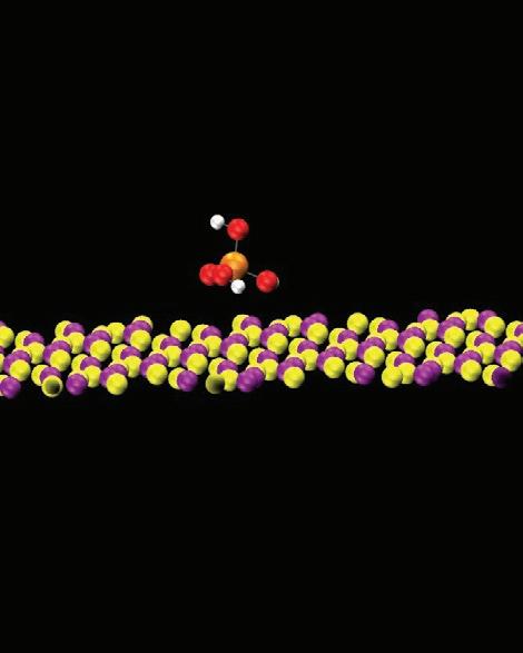
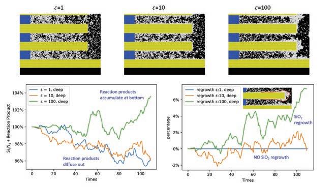
In conventional HSNE applications, hot phosphoric acid (H3PO4) of ~86 wt% at around 160°C is used to etch the SiN sacrificial layers selectively over SiO. In this chemical reaction, phosphoric acid acts as the catalyst to promote the reaction between water and silicon nitride. The products after this nitride etch reaction are SiO2 and NH3. Since this nitride etch reaction is very slow, usually the process is performed in a traditional recirculated etching bath (REB) rather than in single wafer tools to maximize wafer throughput and save costs. In REB applications, reaction products are accumulated in the baths and may redeposit on wafers and form defects. The extension of chemical bath life to further reduce costs usually exacerbates the defect conditions, especially for high loading applications like HSNE. In the HSNE application, one of the main reaction products is SiO2, which is accumulated in the bath gradually during the silicon nitride etch reaction. The SiO2 in the bath will regrow on the silicon oxide layers causing a shift of their critical dimensions and nonuniform etching of silicon nitride sacrificial layers.
In such a 3D layered structure, the HSNE is used to remove the sacrificial nitride layers for the deposition of word line materials (W or Mo) (Figure 5). In 2022, almost all leading 3D NAND manufacturers were able to manufacture 3D NAND flash memories of >150 layers in high volume. In 2023, it is expected that these manufacturers will continue to push the number of layers to 200 and above. However, as the number of layers continue to grow, the aforementioned new issues resulting from high AR and nano-confinement will manifest and gradually dominate.
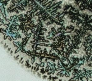
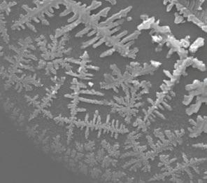
A typical phenomenon observed in HSNE is illustrated in Figure 6. The SiO2 accumulated in the chemistry tends to regrow on the top of the silicon oxide layers and form match-like morphologies. In addition, because of nonuniform distribution of etchant concentration across the deep trench, etching rates in the top layers are usually higher than those in the bottom layers, resulting in obvious nonuniform etch profiles from top to bottom after long processing times. These issues will become even more severe as the number of layers increases and the thickness of SiO/SiN pairs decreases in future technology nodes. Entegris proposes to address these challenges by developing formulated HSNE chemistries optimized for specific application conditions and device structures. Therefore, understanding the mechanisms and processes of silicon oxide regrowth in HSNE is critical.
Entegris, Inc. | 2022 Scientific Report 16
Figure 4. In advanced 3D NAND flash processes, the industry seeks to increase memory capacities by continuously adding layers.
30 0 + SiOx Oxide_N+1 W_N Oxide_N W_N-1 Oxide_N-1 W_N-2 Oxide_N-2 W_N-3 SiOx Oxide_N+1 Oxide_N Oxide_N-1 Oxide_N-2
Figure 5. The HSNE is used to remove the sacrificial nitride layers for the deposition of word line materials (W or Mo).
In the conventional approach, to develop a viable formulated chemistry for HSNE requires intensive investments and serious commitments from both the chip manufacturers and solution providers. Chip manufacturers need to use their precious tool time to prepare test structures and validate the performance of chemistries under high-volume manufacturing (HVM) conditions, while solution providers need to be equipped with capabilities to verify etch performance, defect performance, effects of bath life, effects of chemical shelf life, and other properties of a variety of prototype formulations on both coupons and whole wafers to identify the most appropriate prototype formulations for chip manufacturers’ evaluations. Since the overall evaluation costs are high and cycle times are long, it is highly valuable for solution providers to explore methodologies that more efficiently screen viable solutions and improve trial success rates.

RESULTS OF USING MULTI-SCALE MODELING AND SIMULATION TO MAKE DISCOVERIES


Multi-scale modeling and simulation approaches based on MD are introduced to help scientists and chemists understand the mechanisms of different formulations at a very fundamental level and acquire new insights into directions for formulation design. The first step in building a multi-scale model is to understand the influences of key parameters that are used to describe the behaviors of a system. In HSNE, such parameters include diffusion, etch, and adsorption rates of reaction products in various formulations under different boundary and initial conditions. Unfortunately, among the three key parameters only the etch rate can be measured directly through experimental design. Diffusion and adsorption rates of reaction products in nano-trenches, however,
can hardly be observed and measured by existing techniques. For such parameters that cannot be obtained easily, MD can be used to estimate them computationally at lower costs and faster speeds (Figure 7). As the HSNE system is too huge to be modeled or simulated by MD practically within a reasonable computation time using ordinary workstations or computer clusters, our next step is to reduce the order of modeling and simulation without sacrificing the key attributes of the system by coarse-graining techniques to reduce the scale of computation.
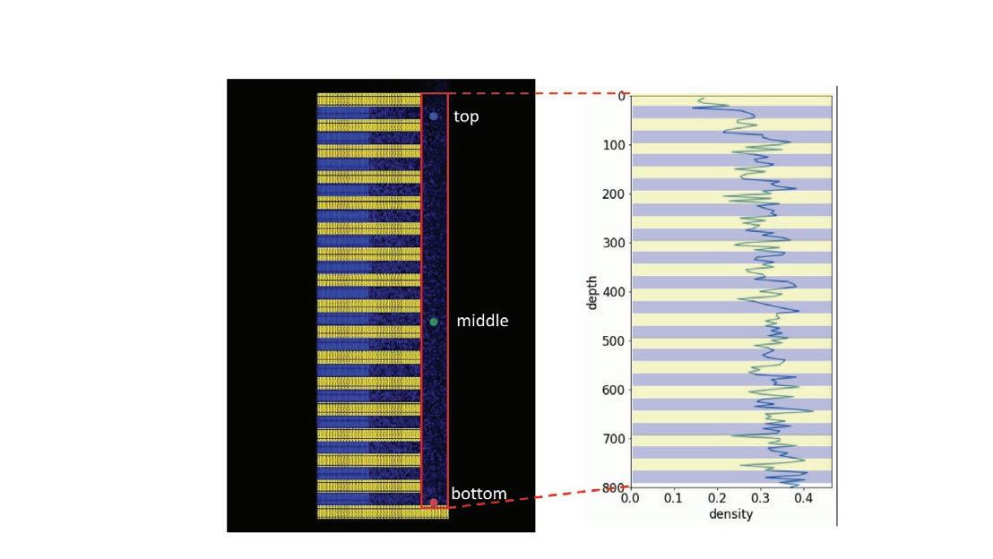
The simplified coarse-grain model is trained to ensure its key attributes (adsorption and diffusion in this case) are aligned with those derived from the finer MD model (finer trains coarser). With the coarsegrain model established, the relative performance of different formulations in this huge HSNE system can be compared virtually. For example, with the coarsegrain model we are able to observe the development of a concentration gradient of reaction products along the vertical trench over time (Figure 8), which suggests that accumulation of reaction products in the vertical trench due to inefficient diffusion may be responsible
Entegris, Inc. | 2022 Scientific Report 17
Figure 6. The SiO2 accumulated in the chemistry tends to regrow on the top of the silicon oxide layers and form match-like morphologies.
—
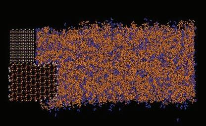
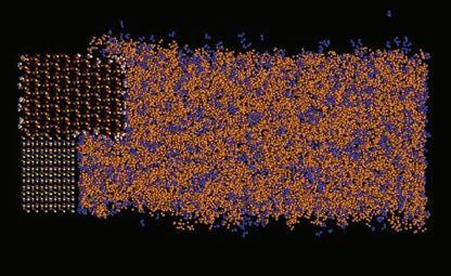
Figure 7. An example of an MD model for the HSNE application.
Figure 8. An HSNE coarse-grain model that illustrates the development of a concentration gradient of reaction products along the vertical trench over time.
Silicon oxide
Silicon nitride
Dept h Reaction Product Density Bottom Middle Top
Phosphoric acid and reaction products
In Figure 9, we demonstrate the simulated performance of different formulations and quantify the regrowth of silicon oxide over time for reference in formulation design or process development. We can then zoom into the molecular view to delve deeper into how atoms and functional groups of different molecules in the system interact with one another (Figure 10) to grasp mechanisms underlying different phenomena and build solid know-how. Combining different information derived from MD-based modeling and simulation, Entegris’ scientists and chemists can acquire the insights and foresight to develop viable solutions much more efficiently.
Design of post-etch residue removal (PERR) formulations for complex 3D structures with HAR is another potential application of MD in advanced semiconductor processes. In conventional BEOL dual damascene processes, special PERR formulations must be applied to remove the residues after dry etch (Figure 11). In PERR formulations the types and concentrations of functional additives such as etchants, solvents, pH adjusters, and inhibitors must be carefully controlled to remove the polymerized nonvolatile residues without corroding the exposed metal surfaces and corresponding liner, barrier, or etch stop layers. Currently, the first few “minimum viable formulations” are usually developed based on their effects on structure-free planar coupons of different materials concluded from laboratory beaker tests. The formulation developers then need to prepare drums of samples for customers’ evaluations in real processes and get customer feedback on performance and defectivity for reference in adjusting formulations for the next on-site evaluation. These iterations repeat until a satisfactory formulation is identified.
Entegris, Inc. | 2022 Scientific Report 18
Figure 9. Quantifying the regrowth of silicon oxide over time in the HSNE application with coarse-grain models based on MD.
Figure 10. An example to explore potential reaction mechanisms based on radial distribution functions (RDF) of particles (atoms, molecules, colloids, etc.) of interest derived from MD.
Time Condition 2 Condition 3 Condition 1 Degree of Oxide Regrowth Radial Distance (Å) RDF (Å –3 ) Radial Distance (Å) RDF (Å –3 ) Si to P N to P N to OH N to H Si to H Si Om OH P H N Formulated Chemistry Dielectric Metal Post-etch residues Etching Stop Layer
Figure 11. A schematic expression of post-etch residue removal (PERR) applications in BEOL.
There are several intrinsic issues with this process. First, the cycle time of the whole process is very long, and the costs very high for both formulation developers and customers. Second, the formulation developers design formulations based on coupon tests without actual post-etch residues, which can result in significant cleaning performance deviations compared to real processes. In addition, the necessity to co-optimize the PERR formulation and the dry etch recipes dynamically during a customer’s R&D process further complicates the situation. Third, the behaviors of formulations in complex 3D nanostructures can hardly be captured by laboratory coupon tests. Without knowing the behaviors of components of a formulation in nanostructures, it’s difficult to determine how to change a formulation even with performance and defectivity information of the formulation in real processes. Unfortunately, such uncertainties contributed by nanostructures will continue to grow as customers continue to shrink critical dimensions and increase the aspect ratio of BEOL structures. Therefore, MD is introduced as one of the approaches to mitigate the impacts of these intrinsic issues by improving the accuracy and the success rate of formulation development. Some applications of MD in PERR formulation development are illustrated below.
When developing a PERR formulation, the first uncertainty chemists face is the difference between the performance of the formulation in targeted nanostructures and the designed formulation based on structure-free coupon test results. As the critical dimension shrinks, the deviation from the performance expectation will increase and may cause unexpected side effects. To contain such uncertainties better when formulating a new chemistry, Entegris uses MD to explore potential mechanisms for formulation deviations and their impact at different nanoscales (an example of the model is illustrated in Figure 12).
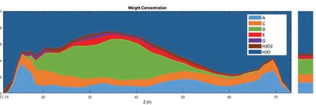
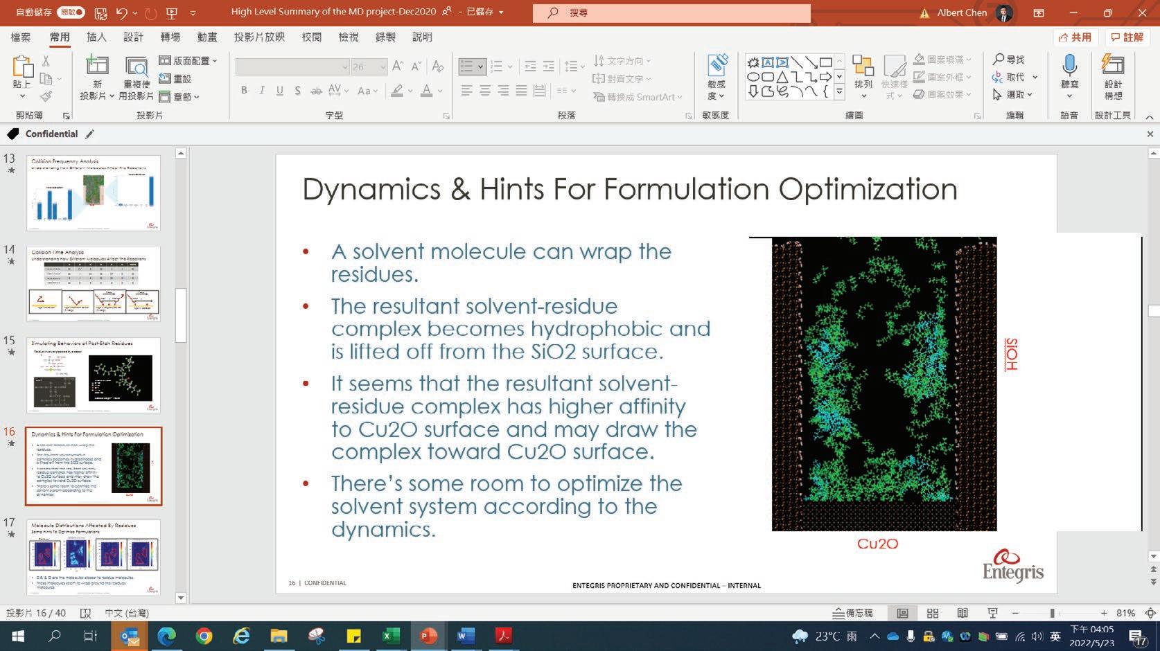
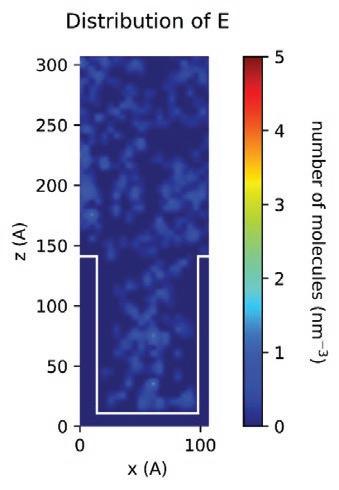
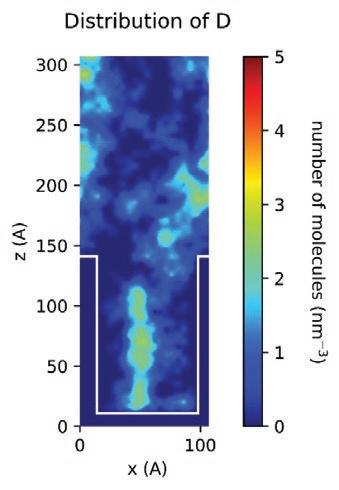
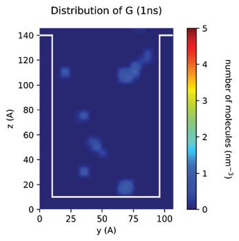
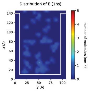
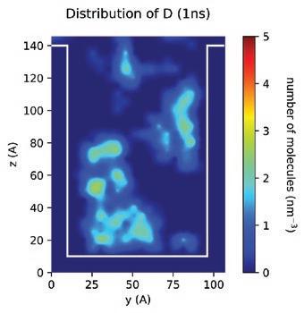
With the MD models established, scientists and chemists can envision more realistic concentration distributions of formulation components at different nanoscales. New insights derived from this information can drive modifications to formulations more accurately to meet targeted purposes or functions in real application scenarios. Figure 13 demonstrates the simulated spatial concentration distribution of different components of an Entegris PERR formulation in a nano-trench. The simulation shows that component D concentrates and forms micelles in the middle of the nano-trench, which eventually may compromise the expected residue removal performance of this formulation. Through MD modeling and simulation, Entegris scientists and chemists can optimize a formulation for real application scenarios virtually before the formulation is evaluated on site using expensive processes.
Entegris, Inc. | 2022 Scientific Report 19
H2O2 G E D C A H2O 1.0 0.8 0.6 0.4 0.2 0 Z (A) Formulation Weight Concentration
Figure 12. Concentration distributions of different components of a PERR formulation in the nano-trench.
Another challenge for scientists and chemists when developing a formulation is the accurate prediction of the relative residue cleaning performance of different formulations in real processes. To make more accurate predictions, a fundamental understanding of the roles of different components in a formulation in the residue removal process is necessary. In this regard, MD can help us in various ways. For example, in one approach various hypothetical “standard” residue molecules were defined, derived from analytical results, and then used to study the relative residue cleaning efficacy of different formulations as well as the
(blue molecules) from the substrate. If we track the evolution of different components in the process, we can also find that both components E and G are adsorbed to the component-residue complex (Figure 15). The adsorption of component E can enhance the overall lifting force to remove residue from the surface
of component G is not preferable since it is designed to
trench. In this simulation, component G is completely
Entegris, Inc. | 2022 Scientific Report 20
Figure 13. Simulated spatial concentration distribution of different components of an Entegris PERR formulation in a nano-trench. The simulation shows that component D concentrates and forms micelles in the middle of the nano-trench, which eventually may compromise the expected residue removal performance of this formulation.
The potential applications of molecular dynamics are ubiquitous and the only limitation will be imagination.
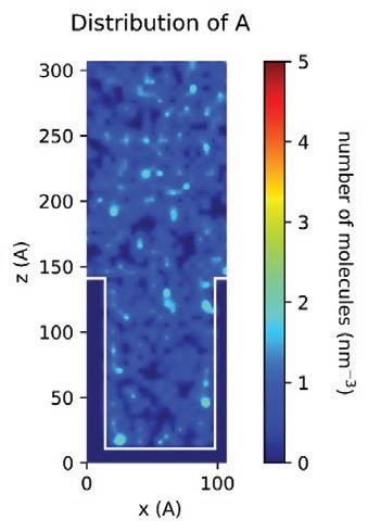
Distribution of A X (A) 5 4 3 2 1 0 Z (A) Number of Molecules (n m –3 ) Distribution of C X (A) 5 4 3 2 1 0 Z (A) Number of Molecules (n m –3 ) Distribution of D X (A) 5 4 3 2 1 0 Z (A) Number of Molecules (n m –3 ) Distribution of E X (A) 5 4 3 2 1 0 Z (A) Number of Molecules (n m –3 )
FUTURE APPLICATIONS AND MODELING AND SIMULATION
—
MD can also be used in a variety of other material development areas. In the microcontamination control area, MD can be used to study the removal efficiency of different media or surface modifications for different contaminants under different process conditions. For area selective deposition (ASD), MD can be used to assess the deposition, selectivity, blocking, stability, and performance of molecules used to form self-assembled monolayers (SAM) on different substrates. In chemical mechanical planarization (CMP) applications, MD can be used to predict the results of modifying slurry abrasive particles with different functional modifiers and the behaviors of modified abrasive particles on targeted substrates. Even in traditional computational fluid dynamics (CFD) applications that have been widely adopted, MD can be used to computationally estimate thermal dynamics, fluid dynamics, or mechanical properties of materials when the properties of interest cannot be obtained easily through experiments. Potential applications of MD or other similar computational approaches at Entegris are ubiquitous and the only limitation will be imagination. We will continue to develop new capabilities in computational chemistry to catalyze knowledge development and generation and lay the foundation for Entegris’ science-based product development process.
References
1 A. Okuyama, S. Saito, Y. Hagimoto, K. Nishi, A. Suzuki, T. Toshima, H. Iwamete, Impact of electrostatic effects on wet etching phenomenon in nanoscale region, Solid State Phenomena, Vol. 219, pp 115-118 (2015).
2 D. Bottenus, Y.J. Oh, S.M. Han, C.F. Ivory, Experimentally and theoretically observed native pH shifts in a nano-channel array, Lab on a Chip, 2009, 9, 219.
3 G. Vereecke, A. Darcos, H. Iino, F. Holsteyns, E. Altamirano Sanchez, Wetting of deep hydrophilic nanoholes by aqueous solutions, Microelectronic Engineering, Volumes 239–240, 111515 (2021).
4 K. Mawatari, N. Harada, K. Ikeda, Y. Kazoe, T. Kitamori, Liquid Properties in Extended-nano Channels: Substrate material, 19th International Conference on Miniaturized Systems for Chemistry and Life Sciences, 1142-1144 (2015).
Entegris, Inc. | 2022 Scientific Report 21
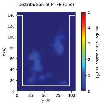
Figure 15. Tracking the evolutions and interactions of different components in a PERR formulation can provide insightful information for formulation development.
Residues X (A) 5 4 3 2 1 0 Z (A) Number of Molecules (n m –3 ) Distribution of D (1ns) X (A) 5 4 3 2 1 0 Z (A) Number of Molecules (n m –3 ) Distribution of E (1ns) X (A) 5 4 3 2 1 0 Z (A) Number of Molecules (n m –3 ) Distribution of G (1ns) X (A) 5 4 3 2 1 0 Z (A) Number of Molecules (n m –3 )

MODIFYING POLYMER SURFACES FOR CONTAMINATION CONTROL Challenges

and Opportunities for Improved Device Yield
Authors: Jad Jaber, Ph.D.
Tetsu Kohyama Aravind Vasanthakumar
Metal contaminants are notorious yield detractors throughout semiconductor unit processes. For example, metallic contaminants found in photolithography materials can create cone defects, resulting in the potential for leakage.1 Because these contaminants are so hard to detect, it is extremely difficult to pinpoint their root cause and identify opportunities to remove them. Clean chemicals used to process semiconductors experience many contamination opportunities between their final quality control checks at the end of manufacturing and dispense onto a wafer. The complexity of the interactions of contaminants and the functional components in semiconductor chemicals is an important consideration when designing removal methods.
Entegris, Inc. | 2022 Scientific Report 23
As the number of contaminants grows and the size of these contaminants shrink, it is increasingly difficult to find a single solution to address the challenge. One solution is through the modification of polymer surfaces to target the removal of specific contaminants, like metals. This becomes even more challenging in photolithography, for example, when metal-oxide photoresists are introduced into high-volume manufacturing, whereby metals that enhance etch resistance must remain in the formulation, while specific metal contaminants must be removed. Here we explore the means to remove metals from photochemicals as an example of the type of work that is needed to target different types of contaminants from a wide range of semiconductor chemicals.
IMPORTANCE OF CONTAMINATION CONTROL IN PHOTOLITHOGRAPHY
Extreme ultraviolet (EUV) lithography is expected to enable a more efficient semiconductor manufacturing process by reducing the number of lithography steps compared to a 193 nm immersion process.2 This promise is hampered by the constraint of a low number of photons per energy dose3 and the exponential increase in the number of defects observed when transitioning from a 7 nm node to the dimensions associated with a 5 nm node or lower.4
Novel photoresists have been under development to improve the photon capture efficiency and increase productivity. One such formulation utilizes copolymers
of acrylate and phenol.5,6 Phenol groups play an important role in addressing stochastic issues in EUV lithography.7,8,9 Because the quantity of photons varies from shot to shot, acids are generated via secondary electron release after phenols absorb photons.10,11 This is different from standard chemically amplified resist systems that are used in ArF processes. Therefore, phenols are important to enhance resist sensitivity with small numbers of photons.12 Unfortunately, while phenols can improve sensitivity, they have a negative impact on defectivity as they may be a source of microbridge defects. Since phenol moieties are less soluble than acrylates, phenol-rich polymer chains can remain as aggregates post development. When aggregated, these chains are not easily developed or rinsed away, leaving a bridge defect on the wafer surface between fully developed patterns (Figure 1).
Trace metal contamination is another source of defects in novel photoresists that can influence device performance and result in low yield.1 Mobile metal ions can diffuse into the silicon oxide layer and are not effectively removed by sulfuric peroxide mixture (SPM) etch.13 Metallic contaminants can also act as nucleation sites around which resist polymer chains may aggregate and result in gate leakage.14
The complexity of the interactions of metal contaminants and the components in photochemicals is an important consideration when designing removal methods. This challenge increases when the uniformity of the photoresist comes into play, whereby resist chains that enhance sensitivity must remain, while defect-causing resist chains must be removed.
Entegris, Inc. | 2022 Scientific Report 24
Figure 1. Hypothesis on defect generation mechanism.
Phenol groups Acrylate groups
Weak interaction to stabilize in TMAH TMAH Development Process Bridge defect generation After Spin Dry Aggregation DI Water Rinse
There are many more than two types of contaminants to consider when exploring contamination control in photoresists. Systematically identifying root cause is time and resource consuming. While a single solution to address all contaminants is desirable, it is not realistic. Therefore, different methods must be designed to address each contaminant type. Significant efforts have been made to address metallic contaminants, which pose the biggest risk to circuit performance and yield.
CURRENT STATE OF CONTAMINATION REMOVAL TECHNOLOGIES
There are several techniques to reduce metal contamination load in a solution, such as electrodialysis,15 liquid-liquid extraction,16 metal organic frameworks (MOFs),17 and ion exchange adsorbents.18,19 However, most of these technologies were developed for waste or brackish water purification applications and have limited utility in the more stringent field of photochemicals.
Ion exchange media is by far the most used technique for the purification of photochemicals.20 It can be in the form of porous polymer resins packed in a column or modified filtration membranes. Fluid flow in a packed column tracks the path of least resistance which is the interstitial volume formed by the space between the resin. To remove metal contamination, ions in the fluid must diffuse and interact with the ion exchange groups on the crosslinked resin surface. Since the internal surface of the resin represents the larger fraction of the surface area available for adsorption, the flow rate must be kept low to enhance the mass transport process and increase the binding capacity of the packed bed. This is especially important in the case of highly crosslinked resins with poor accessibility and viscous photochemicals, both of which can negatively impact the diffusion rate of the metal ions and consequently their extraction efficiency. Increasing contact time with the resin, either through recirculation or flow rate reduction, negatively impacts process efficiency and throughput. Moreover, it is labor- and time-intensive to pack, clean, and validate packed resin columns.
The shortcomings of packed bed resins can be offset by using filtration membranes, which offer faster setup time, flexible processing, and easy handling. These are highly convective media with optimized membrane morphology, pore size, and functionality to enable fast mass transfer and easy access of metal ions to all available surface area. In one approach, the surface of a microporous ultra-high molecular weight polyethylene (UPE) membrane can be functionalized with application-specific functional groups that act as adsorbents for metals without releasing counter ions into the solution.21,22
UPE filters are widely used in photochemical filtration because of their chemical inertness, cleanliness, and ability to be modified. Unlike packed bed chromatography columns, where good extraction efficiency comes at the expense of reduced process throughput, all the functional groups on a filtration membrane are in the convective flow of the liquid, and, therefore, there are no diffusional mass transfer limitations.
A few Entegris products have entered the market that extract metal contaminants from solvents with high efficiency.22 However, utilizing this technology in photoresist formulations reveals a different picture compared to pure solvent. The interaction between the other components in the resist formulation and membrane surface functional groups creates a negative impact on photoresist performance and metal removal efficiency. Figure 2 highlights the filtration of a solution of photo acid generator (PAG) in propylene glycol methyl ether acetate (PGMEA)/ethyl lactate containing 1.2 ppb of native metals using two products, A and B. Total metal removal efficiency did not exceed 70% with almost no extraction of Zn and 100% extraction of Fe (Figure 2a).
Entegris, Inc. | 2022 Scientific Report 25
—
100 80 60 40 20 0 All other metals Zn Fe Metal Removal (% ) New Molecule Product A Product B
Figure 2a. Metal reduction in a PAG solution using product A, product B, and a 0.2 µm UPE membrane modified with a new molecule.
Figure 2b shows the results of a wafer coated with a photoresist generated from the filtered PAG solution and other components. A shift in critical dimension was observed when compared to a formulation of similar components but with unfiltered PAG. This was possibly due to the extraction of some amount of the PAG by surface functional groups on the membrane.
This result drove research into the development of a new molecule that was even more highly selective to the metal contaminant and no other formulation component. A 0.2 µm UPE membrane was modified with a proprietary molecule and used to purify the PAG solution, as described before. Figure 2a shows that the total metal removal efficiency of this membrane exceeded 90% with an impressive removal efficiency for both Fe and Zn. At the same time, no change in the pattern size created by using a resist formulation comprising the purified PAG solution, was observed (Figure 2b). This indicates high selectivity of the membrane for metal contaminants without interfering with other components in the formulation.
LOOKING AHEAD
Innovative filtration technologies are needed to address the most stringent defect targets and eliminate defectcausing species before they negatively impact semiconductor production efficiency. Adsorptive retention mechanisms boost membrane filtration efficiency and can be an effective tool for contamination control in photolithography solvents. Functionalized membranes are likely to show a similar benefit in more complex, multicomponent formulations where selectivity toward metal contamination and lack of interaction with other crucial components in the system are desirable. While
the example in photolithography shows promising results, additional research is needed to address the many chemicals used in the semiconductor manufacturing process and to further address the many different types of contaminants, like phenol aggregates.
Entegris constantly researches opportunities to tailor filtration for the emergence of new innovative photochemicals. However, such experimentation comes at the price of laborious processes requiring several iterations, which adds to the cost of developing advanced purification solutions. To counter these challenges, methods that leverage computation along with experiments are being developed. One such method is based on a probable correlation of metal retention by ligands with complexation energy of the resulting ligand-metal complex. Using this resulting parameter, ligands can be screened and ranked against metal ions of interest in a solution at a given pH. Presently, a large amount of experimental data is needed for validation purposes and to further understand the limitations of such computational methods.
The same methodology can be extrapolated to larger databases of ligands and metals in solutions or solvent at specific pH levels. User-friendly tools can be designed such that most of the work is automated, where the user initiates the computations by providing appropriate inputs. Experiments can then be narrowed down to a smaller set of trials to identify a final combination tailored for the application, thus saving several months of costly work.
Validation of such computational methods is an important part of the development cycle. In the validation step, the ligands are ranked against the metal ion of interest. In addition, residual concentrations of metal ions in solutions from experiments that have been treated with the same list of ligands are ranked. The rankings from simulations and experiments are then compared to evaluate the simulations. Outcomes from such analysis have shown that additional experimental factors need to be considered to make the simulations robust and on target. Factors include the structure of the membrane used, initial distribution of metal ion species, and ratio of available ligands to metal ions species within the solution. These factors affect the process of metal removal rates and models need to be tuned in to better correlate with experiments.
Entegris, Inc. | 2022 Scientific Report 26
Figure 2b. Sensitivity shift in resist formulation comprising the PAG solution purified using a new membrane, product A, and product B. Connecting line is a guide for the eye.
2.4 1.6 0.8 0 -0.8 -1.6 -2.4 -3.2 New Molecule Product A Product B Sensitivity Shift (% )
Currently, advances in computational resources combined with machine learning algorithms create opportunities for scaling the screening quickly and identifying potential solutions. Such efforts are already in progress and have been successfully demonstrated.23 With such methods ligands can also be synthesized with deep-learning algorithms based on inverse design models.24 These find a place in cases where there are no readily available ligands or a need to tailor solutions for specific applications.
CONCLUSION
Stochastic defects pose an ever-greater problem to EUV photolithography success with sub-16 nm device features size. Chemical suppliers continue to make significant efforts to improve photoresist chain uniformity and create high-quality materials that address defectivity challenges. These manufacturers cannot accomplish these goals without innovative filtration solutions. Entegris – like all members of the semiconductor supply chain – leverages our scientists’ and engineers’ creativity and innovative ideas to find new solutions to target selective removal of postdevelopment aggregation-prone resist chains helping to improve material quality and device yield.
As technology changes, we must all adapt. While the tools of the past have enabled Entegris to demonstrate the ability to tailor membranes to address particular contaminants, it is time to seek new sources of inspiration and analysis, such as machine learning, to create the filters that are likely to show a similar benefit in more complex, multicomponent resist formulations where selectivity toward metal contamination and lack of interaction with other crucial components in the system, such as polymers and metal oxide catalysts, are desirable. Filters of the future that address these complex contamination challenges, as well as those faced by other unit processes, will only be created by combining deep technical knowledge, collaborations with the semiconductor value chain, and advanced computational resources.
References
1 P. J. Ward, J. Electrochem. Soc. 129, 1982, 2573-2576.
2 S.K. Moore, IEEE Spectrum, 05 January 2018. https://spectrum.ieee. org/semiconductors/nanotechnology/euv-lithography-finallyready-for-chip-manufacturing
3 D. De Simone, M. Mao, F. Lazzarino, G. Vandenberghe, J. Photopolym. Sci. Technol. 29, 2016, 501-507.
4 P. De Bisschop, J. Micro/Nanolith. MEMS MOEMS, 16, 2017, 300-317.
5 Satinder K. Sharma, et al., Evaluation of high-resolution and sensitivity of n-CAR hybrid resist for sub-16nm or below technology node Proc. of SPIE Vol. 10583 (2018).
6 Thomas, W, et al., Evaluation of EUV resist materials for use at the 32 nm half-pitch node, Proc. of SPIE Vol. 6921 (2008).
7 Fallica, R, et al., Dynamic absorption coefficients of CAR and non-CAR resists at EUV, Proc. of SPIE Vol. 9776 (2016).
8 Furutani, H. et al., Novel EUV Resist Materials for 7nm Node and Beyond, Journal of Photopolymer Science and Technology Vol. 31 No.2, 201-207 (2018).
9 D. Deanilo Simone et al., The Path to Better Understanding Stochastics in EUV Photoresist, Journal of Photopolymer Science and Technology Vol. 31 No. 5, 651-655 (2018).
10 A. Narasimhan et al., What we don’t know about EUV exposure mechanism, Journal of Photopolymer Science and Technology Vol. 31 No. 1, 113-120 (2017).
11 Y. Vesters, et al., Sensitizers in EUV chemically amplified resist: mechanism of sensitivity improvement, Proc. of SPIE Vol. 10583 (2018).
12 J. Torok et al., Secondary electros in EUV lithography, Journal of Photopolymer Science and Technology Vol. 26 No. 5, 1625-634 (2013).
13 R. Vos, M. Lux, M. Meuris, P.W. Mertens, M.M. Heyns, R. Ramage, Solid State Phenom. Ultra Clean Processing of Silicon Surfaces, 1998, 65-66, 279-282.
14 Umeda, T., et al., Defect reduction by using point-of-use filtration in a new coater/developer, Proc. SPIE 7273, 727374B (2009).
15 K.L. Gering, J.F. Scamehorn, Sep Sci Technol. 23, 1988, 2231-2267.
16 F.L. Moore, Anal. Chem. 1965, 37, 10, 1235-1239.
17 P.A. Kobielska, A.J. Howarth, O.K. Farha, S.N. Nayak, Coord. Chem. Rev. 2018, 358, 92-107.
18 M.V. Mier, R.L. Callejas, R. Gehr, B.E.J. Cisneros, P.J.J. Alvarez, Water res. 2001, 35, 373-378.
19 Z. Reddad, C. Gerente, Y. Andres, P. Le Cloirec, Environ. Sci. Technol. 2002, 36, 9, 2067-2073.
20 D. Capitanio, Y. Mizuno, J. Lee, Proc. of SPIE 3678, 1999, 684-688.
21 V. Goel, A. Wu, J. Braggin, Proc. of SPIE 10960, 2019, 1096011-17.
22 J. Jaber, J. Hamzik, N. Filipancic, J. Brewster, A. Xia, Proc. of SPIE 11326, 2020, 1132613-20.
23 J.W. Barnett, C.R. Bilchak, Y. Wag, B.C. Benicewicz, L.A. Murdock, T. Bereau, S.K. Kumar, Designing exceptional gas-separation polymer membranes using machine learning, Science Advances 2020, 6, https://www.science.org/doi/10.1126/sciadv.aaz4301
24 K. Kim, S. Kang, J. Yoo, Y. Kwon, et al, Deep-learning-based inverse design model for intelligent discovery of organic molecules, npj Computational materials, 2018, 67, https://www.nature.com/articles/ s41524-018-0128-1
Entegris, Inc. | 2022 Scientific Report 27

SEMICONDUCTOR MATERIALS SUPPLY CHAIN FOR 2030
 Authors: James A. O’Neill, Ph.D. Wenge Yang, Ph.D.
INTRODUCTION
—
The semiconductor industry has completed a transformation in the last five years from a stable-growth industry to a high-growth industry, highlighted by its double-digit annual post-pandemic growth rate since 2020. With multiple secular growth drivers in place, such as 5G, artificial intelligence (AI), internet of things (IoT), big data, and electric vehicles/autonomous driving, it is well accepted that semiconductor long-term growth will be here to stay.
With the semiconductor industry historically growing at 2× the rate of global gross domestic product (GDP), it is now a consensus that the industry will reach sales of one trillion dollars by 2030, roughly doubling in size within a decade (Figure 1). While this is great news for the semiconductor supply chain, it is a massive challenge for the industry’s entire ecosystem to scale in support of such rapid and significant growth.
Entegris, Inc. | 2022 Scientific Report 29
For the world to reach semiconductor shipment levels of $1T, It is estimated that the industry will need to produce 20 billion square inches annually, an increase of 67% over the 12 billion square inches of wafers produced in 2020. This requires an addition of 77 new 300 mm mega fabs with 100,000 wafer starts per month capacity, a very tall order that requires a massive amount of capital investment to achieve (Figure 2). The expected growth for semiconductor materials to support a $1T level is even more staggering, with estimated materials consumption more than doubling from 2020 to 2030, exceeding the industry. Our calculations indicate that the anticipated pace of expansion will require growth across all key materials segments, providing substantial opportunities for semiconductor materials suppliers, but also posing several significant challenges to the materials supply chain.
AGGRESSIVE CAPACITY EXPANSION


To more than double semiconductor materials shipments in one decade, materials suppliers must be very aggressive in expanding capacity. The industry traditionally has operated with a conservative approach to capacity addition, requiring a paradigm change toward timely decision-making and bold actions to add capacity to support such rapid industry growth. For semiconductor materials, in particular, there are increasingly complex factors to consider, such as new demands on the materials that are being ramped in this timeframe, like improved materials purity and reduced materials variability. These demands drive new manufacturing capabilities in the area of robust automation and stringent process control as well as new ways of thinking about materials packaging.

Entegris, Inc. | 2022 Scientific Report 30
Figure 1. 2020 sales at $471B, 2030 sales are projected to be >$1T. Source: Gartner and Entegris estimates.
1200 1000 800 600 400 200 0 1982 1984 1986 1988 1990 1992 1994 1996 1998 2000 2002 2004 2006 2008 2010 2012 2016 2018 2020 2022 2024 2026 2028 2030 2014 Semiconductor Annual
Billions ($ ) Year Figure
10K additional annual MSI Millions of Square Inches of Silicon (MSI) 77 new 100K wafer starts per month (WSPM) fabs Fabs $160B/yr. to build and equip new fabs Capex $100B/yr. WFE market to equip new fabs Wafer Fab Equipment (WFE) Market $20B/2021 to $50B/2030 10% CAGR vs. 7% MSI/Semi Fab Materials
Sales History and Forecast
2. What does a $1T industry mean to the supply chain?
HIGHER MATERIAL PURITY

With the industry producing 3 nm node devices today and chasing the Angstrom era within this decade, material purity requirements will increase significantly. Already, advanced logic processes specify material purity in the ppq regime for metals and the low-ppt level1 for organic contamination. As a basis for comparison, 1 ppq is equivalent to one drop of water flowing over Niagara Falls in a day. This is vanishingly small and nearly undetectable. In addition, the size of a killer defect for a 7 nm technology is less than 5 nm. Yet the detection capability of an on-wafer inspection tool is in the range of 10 – 15 nm. Therefore, most IC manufacturers are operating in the dark. They physically cannot see the defects that can lead to device failure and must rely on downstream electrical testing to identify such defects. This challenges the materials supply chain to manage material purity throughout the ecosystem from raw materials to on-wafer delivery, and it has driven many customers to implement redundant filtration and purification schemes as an insurance policy against the contamination and defects they cannot see. It requires more advanced filtration, purification, packaging, and delivery solutions to maintain purity of the materials, as well as a robust quality control system to sustain the quality of materials from batch to batch.

MANUFACTURING AUTOMATION AND STRINGENT PROCESS CONTROL

Process variability is the bane of any semiconductor process engineer. Rigorous process controls and statistical methods are implemented across the fab to ensure that every process in the fabrication sequence is both centered and controlled within precise limits. As a key input to the process, materials variability must be strictly controlled as well. Increasingly, fab operators require rigorous certificates of analysis (COAs) to ensure that incoming materials hold to their specifications. This is true not only for the final material but also for material ingredients used to formulate the final product. In effect, they seek complete transparency from their supply chain. To achieve such requirements at rapidly increasing volumes, materials suppliers will need to rely on a higher level of automation during synthesis, and more thorough implementation of statistical process controls throughout their manufacturing process.
ROBUST MATERIAL INTEGRITY
Materials packaging is a critical aspect of ensuring the integrity of the product from the point where it is manufactured to where it is used on the wafer. Since the lifecycle of a material may span several months and cover several continents (manufacture in the U.S., use in Taiwan), there are many points along the material’s journey where it may become contaminated or otherwise degraded in quality. It is no longer sufficient simply to make a pure material. The supplier must be able to ensure the integrity of that material from the point of manufacture to the point of use. While filtration and purification methods are increasingly implemented at more points along the supply chain (point of manufacture, sub-fab, point of use), new ideas are required to ensure “constant cleaning” during the period when the material is in a package. Also, most wet chemistries are typically packaged in drums, and as the volume of chemistry increases, the number of drums would be expected to rise as well. However, since most contamination is introduced from the interaction of a material with the surface of its container, there is an opportunity to consider new options that allow shipping increased volumes without increasing the surface area of the packaging (new container geometries). A new approach would have implications for how a material is introduced to the fab, so a comprehensive consideration of the material flow over its lifecycle is required.
Entegris, Inc. | 2022 Scientific Report 31
Figure 3. 1 ppq is equivalent to 1 drop of water flowing over Niagara Falls in 1 day.
There are many points along the material’s journey where it may become contaminated or otherwise degraded in quality. It is no longer sufficient simply to make a pure material.
Vanishingly Small And Nearly Undetectable
SUPPLY CHAIN COMPLEXITY


Today’s advanced logic IC requires 2,000 – 3,000 process steps to manufacture and hundreds of materials to be used at various stages of the process flow. This is a 2× increase compared to the process flow of just a decade ago. With the adoption of the gate all around (GAA) transistor, 3D structures, backside power rails, and new materials for better interconnect schemes, the number and complexity of materials used for semiconductor manufacturing will only further increase. Many of the materials used to fabricate semiconductor devices carry safety, health, and environmental hazards. In addition, raw materials are sourced from many regions around the world, some more stable than others. This requires the materials supply chain to develop much more sophisticated operations and modern data management to handle this vast complexity. In this regard, several factors need to be considered including data transparency, geopolitical risk, and sustainability.
DATA TRANSPARENCY


Doubling semiconductor materials shipments within the decade will demand that scalable supply chain ecosystems become closely knit networks of key customers, suppliers, and sub-suppliers collaborating toward shared advantage. Future ecosystems will be enabled using system-to-system connections with visibility to inventory and work in progress (WIP) across the supply chain, shared and secured with private blockchain clouds. This new way of operating will greatly eliminate waste and minimize overall risk to all partners. The ecosystem model in combination with digitalization further allows for robust and systematic sharing of data to help identify potential issues to both customers and suppliers, dramatically reducing the time to resolve excursion activities, and in many cases, eliminating them before a problem even arises. We must manage massive amounts of data across the supply chain, while ensuring data security, or it will be difficult to achieve the availability, scalability, and quality in the timeframes required. Digitalization provides the visibility and scenario planning for all aspects of the material life cycle, enabled through modeling and/or a digital twin of the supply chain internally as well as downstream. This allows for robust contingency
planning and constant machine-based optimization to create a nimble and flexible supply chain adjusting to rapidly changing scenarios with minimal personnel involvement. A paradigm shift results when people are involved only where they can add value, such as model training, unique situations, or relationship management. Digitalization is not about replacing people with machines, but rather augmenting the abilities of both to work together seamlessly which will enable better and faster decisions.
GEOPOLITICAL RISK
Since the 1990s, many companies have pursued a strategy of outsourcing and lean manufacturing to cut costs. This distributed, low-inventory strategy has the potential of introducing supply chain disruptions from factors largely out of the company’s control. In this context, recent geopolitical conflicts and increased nationalization of the semiconductor industry have forced the materials supply chain to adapt to new geopolitical requirements.
For example, several elements common to the semiconductor industry have been designated as conflict minerals – including cobalt, tantalum, and tungsten – making sourcing decisions a critical factor in any supply chain informed by human rights considerations. Also, the world’s largest reserves of rare earth elements, many of which are used in semiconductor fabrication, are found in China, giving a single country dominance over a critical part of the materials supply chain. In addition, the recent conflict in Ukraine has highlighted the vulnerability of access to materials such as neon and other critical metals within the semiconductor materials supply chain.
Entegris, Inc. | 2022 Scientific Report 32
Figure 4. Tricky geopolitical interplay.
Taiwan Ukraine Russia China
Finally, the global COVID-19 pandemic, particularly pandemic-related shutdowns, highlighted vulnerabilities in critical supply chains that manifest themselves in shortages of key products that depend on semiconductor components, such as automobiles. These challenges and crises accelerated the need for businesses to re-examine both short- and long-term supply chain decisions and forced new supply chain strategies that include sourcing management, logistics and freight optimization, localization of manufacturing and distribution, and sufficient redundancy to minimize the supply risk at specific geographic locations.
SUSTAINABILITY
Climate change is creating disruptions around the world due to extreme weather, rising sea levels, and increasing drought. Materials ubiquitous to the industry like PFAs (per- and polyfluoroalkyl substances) are being regulated by an increasing number of countries. Semiconductor fabs are large consumers of both power and water. All of these factors warrant that sustainability be a major emphasis for semiconductor companies in general, and materials companies in particular, as they ramp production to meet the increased demand for chips. Companies have already begun to set objectives to achieve reduced energy consumption, to consume energy from renewable sources, and to decrease water consumption in their manufacturing processes. In addition, an increasing focus of R&D is to identify alternatives to hazardous or environmentally unfriendly chemistries by developing processes that require less solvent use or replace hazardous materials. And the circular economy is a focus of many materials commonly found in the semiconductor process such as polymer tubing, drums, and filters. In fact, the entire semiconductor industry is prime for a concerted effort to reduce its plastics footprint from packaging to process applications.
This new era of sustainable materials, while a challenge, is by no means limiting the number of options to explore – the technology to manipulate materials
is emerging every day. Chemists in the industry have identified processes that have unlimited recyclability, as well as materials that are inherently safe while also maintaining a clear advantage to their earlier predecessors. Given its overall contribution to the world economy and the ensuing financial benefits that the semiconductor industry has enjoyed, the industry has a responsibility to lead the way in solving the major unmet challenges of our time. This next era of sustainable materials development is an opportunity to establish a legacy of outperforming the industry’s social responsibility while providing our customers with products that are certain to give them an accelerated trajectory to future advances in semiconductor technology.
SUMMARY
The semiconductor industry is rocketing toward the $1T milestone. It’s driven by the demand for chips, the fundamental building blocks that enable so many societal trends that depend on data: autonomous vehicles, ubiquitous communication, artificial intelligence, smart cities, and efficient manufacturing and supply chains. But therein lies an opportunity for the industry that enables this advancement to eat a bit of its own home cooking – to leverage the power of the products it enables to address some of its own challenges. Using computational methods to accelerate development would reduce the consumption of resources and enable more efficiently manufactured designs. Leveraging data to streamline supply lines would improve raw material usage and reduce waste. Automating manufacturing processes and implementing more statistical controls would improve productivity and reduce scrap. Reflecting on the events of the last two years (the pandemic, effects of climate change, global conflicts), there is no better time to apply urgency to addressing the challenges that face the semiconductor materials industry. Looking ahead to 2030 provides ample opportunities to change our practices to ensure wider collaboration and transparency between parties to ease the strain in the supply chain, specifically leveraging technologies enabled by the semiconductors being manufactured.
References
1 https://irds.ieee.org/images/files/pdf/2022/Metals_WP.pdf
Entegris, Inc. | 2022 Scientific Report 33
The entire semiconductor industry is prime for a concerted effort to reduce its plastics footprint from packaging to process applications.

HYDROGEN GAS FOR SEMICONDUCTORS AND CLEAN ENERGY
New Surface Chemistry Challenges
 Authors: Rocky Gipson, Ph.D. Mark Puttock, Ph.D.
INTRODUCTION
Hydrogen is the simplest and most abundant chemical element in the universe, having an atomic number of 1 and normally existing as H2 (gas) in standard conditions. It came into existence in the first second of the big bang and currently comprises about 75% by mass of the normal matter in the universe. The hydrogen atom consists of one proton and one electron in its most abundant isotope 1H.
Entegris, Inc. | 2022 Scientific Report 35
H2 was first produced in the 16th century by the reaction of acids on metals. Henry Cavendish was the first to isolate hydrogen gas and recognize that it produces water when burned, hence the name in Greek “hydrogen” meaning “water forming.” Hydrogen is colorless, odorless, tasteless, and non-toxic but is highly combustible. Hydrogen is less reactive than other naturally occurring diatomic elements such as halogens.

The H-H bond is very strong (dissociation energy 435.7 kJ/mol). The reactivity of H2 is greatly affected by the presence of metal catalysts. Though mixtures of H2 and O2 or air combust readily when heated to at least 500°C (932°F) by a spark or flame, the reaction does not occur at room temperature in the absence of a catalyst. Today, the agricultural industry consumes 55% of global hydrogen to produce ammonia used in fertilizers (Figure 1), while less than 10% is used for other applications like semiconductor manufacturing, hydrogenated food production, metalworking, welding, flat glass production, and energy storage. The forecast for the overall use of hydrogen and the importance of hydrogen for the world’s economy is growing.

New applications exist for hydrogen ranging from liquid hydrogen fuel using modified jet engines for aviation2 to fuel cells for trucks,3,4,5 buses,6 and trains.7 Airbus2, as an example, has several concept aircraft called ZEROe, each powered by hydrogen combustion through modified gas turbine engines. Airbus announced their ZEROe demonstrator aircraft in February 2022. The goal is to release the first zero emissions commercial aircraft by 2035.

Here we will discuss only current and future hydrogen challenges in semiconductor manufacturing and the evolving energy ecosystem. Specifically, we will examine the approach to purity requirements in those sectors, how they work today, and the likely evolution of these needs and challenges.


Entegris, Inc. | 2022 Scientific Report 36
Figure 1. Today, only a small percentage of hydrogen is used for green energy.1
Global Hydrogen Consumption
25% Petroleum Refining Other, Including Green Energy Storage 10% 55% Ammonia Production Methanol Production 10%
2040 2030 2020 Creation of zero-emissions development centers 20 21 Anticipated first flight test 20 25 ZEROe demonstrator project introduced 2022 Estimated entry-into-service of ZEROe 2035 ZEROe Timeline
by Industry
Figure
2. Airbus is developing a hydrogen-based aircraft.2
HYDROGEN USED IN SEMICONDUCTOR MANUFACTURING
Semiconductor devices are ubiquitous today and will be into the future. This industry is predicted to reach a trillion dollars (U.S.) by 2030. Microchip fabrication is a series of basic processes: patterning, deposition, etching, doping, all in a precise manner and sequence. Due to the nanoscale of semiconductor chip devices, even parts-per-billion (ppb) levels of contamination can result in device failure immediately in manufacturing as yield loss or later in use as poor reliability.8 Hence, most processes have very stringent purity requirements and sensitivity to specific contaminant types.
Hydrogen is considered a bulk gas in semiconductor manufacturing, employed in many areas of the ecosystem. Key examples in Table 1 show how H2 is utilized in many semiconductor fabs.
STEP DESCRIPTION
Epitaxy Precise growth of silicon layers
Annealing Heating to ca. 100°C repairs silicon from doping implantation steps
Deposition Steps that introduce thin films to the surface of the wafer
Ion implantation The doping of semiconductor layers to enable device functionality
EUV lithography The process of defining a pattern in a photosensitive material
Contaminants have been grouped into standardized classes as shown in Table 2 along with typical concentrations found in a supply of 99.999% H2 (termed “5N” or “five nines”). From the initial 5N purity, typical outlet purity requirements are also provided per class.
Acids NOX , SOX , organic acids
NO2, SO2 0.1 – 1 ppmv (<1 pptv)*
Atmospherics CO2, CO, O2, N2
Bases
Amines, silazanes
KEY ENABLING PROPERTY OF H2
Hydrogen as a chemical reducing agent in growth
Hydrogen transfers heat and removes unwanted oxide layer
Hydrogen incorporation into thin films increases resistivity
In the ion source, hydrogen blocks the transport of W, increasing the stability and lifetime of the tool
Liquid Sn is used to generate EUV radiation and may be deposited inside the system; hydrogen cleans up the residual Sn
Table 1. Semiconductor steps that utilize hydrogen.
Metals Fe, Mn, Mo, Ni, Cr, others
0.1 – 1.0 ppmv (<100 pptv)
NH3 1 – 100 ppbv (<1 ppbv)
Fe, Cr 1 – 100 ppbv (<1 ppbv)
Moisture H2O 0.1 – 25 ppmv (< 1 ppbv)
Organics
Condensable (45 – 100 amu)
Toluene 0.1 – 2 ppmv (< 1 pptv)
Non-condensable (>100 amu) Decane
Refractory compounds
Halogenated organics, silicon compounds
Hexamethyldisiloxane (HMDSO)
< 100 ppbv (<1 pptv)
Entegris, Inc. | 2022 Scientific Report 37
CLASS TEST SURROGATE TYPICAL CONCENTRATION IN
CLASS
5N H2
* Typical purity requirements.
Table 2. Semiconductor gas contaminant classes.
PURIFICATION NEEDS OF H2
Surface science plays a major role in the purification of hydrogen. Several surface-based technologies are available to purify hydrogen for use in the semiconductor. For any given semiconductor process, the appropriate solution is a balance of purity needs, scale, and cost. We provide a brief description of the most widely adopted technologies and compare technologies in Table 3.
ADSORPTION
Adsorption-based purification employs porous materials, generally in a packed-bed configuration. Depending on the need, current products contain adsorbent materials (media) that can range from zeolites and activated carbon, to metal organic (MOF) or covalent organic (COF) frameworks. Immobilizing gaseous contaminant molecules on the media surface involves weaker forces of physical attraction (physisorption), as well as stronger chemical bonds (chemisorption). Adsorbent materials are evaluated on selectivity, the ability to remove molecules preferentially in the presence of others, and porosity of the form factor. Suitable adsorbents should be readily regenerable, meaning once they have reached end-of-life, performance can be restored by the application of heat and additional gas to desorb contaminants.
CRYOGENICS
Because the adsorption process is generally exothermic, or heat generating, colder temperatures improve performance substantially. For example, the use of liquid nitrogen as a coolant (-196°C) allows for much more favorable separations resulting in removal of unwanted contaminants, such as argon, that have no media affinity near room temperature.
Ultimately, the best performance of adsorbent-based technology relies on understanding and optimization of the gas-solid mass transfer process.
GETTER
Gettering technology has been invaluable for decades, enabling such pioneering developments as the vacuum tube. When heated, the getter material – a solid metal alloy – becomes very reactive and accumulates impurities through a chemisorption mechanism. Though most getter development was done targeting vacuum or noble gas applications, zirconium-based getter purifiers are widely used for the purification of hydrogen, especially when methane and nitrogen removal are required. During the high-temperature removal of impurities, corresponding nitrides, carbides, and oxides form on the surface of the alloy, then migrate to the center of the solid. Once the getter has completely reacted, it must be replaced. Due to the high reactivity of getter alloys, practical safety concerns limit the flow rating to 300 m3/hr.
Entegris, Inc. | 2022 Scientific Report 38 TYPE REQUIRED INLET PURITY FLOW RANGE IMPURITIES NOT REMOVED RELATIVE COST NOTES Adsorber 4.5-5N 0.01 – 1,000 m3/hr N2, CH4, noble gases $$ Least expensive, best scalability Cryogenic adsorber 4N 20 – 1,000 m3/hr Helium $$$ Requires liquid N2, suitable for high flows Getter 6N 0.1 – 300 m3/hr Noble gases $$$ Excellent performance, cleaner gas needed Palladium 3.5N 0.1 – 100 m3/hr None $$$$ Removes all impurities, insensitive to gas quality, high cost
Table 3: Comparison of semiconductor hydrogen purification technologies.
PALLADIUM
Palladium metal has the uncommon property of being permeable to hydrogen. Under certain conditions, the hydrogen molecule binds to the Pd surface and dissociates into hydrogen atoms, which migrate through the metal crystal lattice to recombine on the opposite side (Figure 3). Because this permeation mechanism is exclusive to hydrogen, it is the only 100% selective purification technology. Given sufficient surface area, palladium membrane technology can tolerate much higher impurity levels than other techniques, which makes it attractive for reclaiming and recycling hydrogen from process effluent and other H2 waste streams. To prevent impurity buildup on or near the membrane surface, a small portion of the incoming H2 flow, typically 2%, is continuously vented along with the impurities.
commitment to target global CO2 emissions reduction by 45% by 2030 relative to 2010 level and to net zero around midcentury.9 To varying degrees, all regions of the world have an energy plan including hydrogen, for example (1) the EU commission10 set out investments between Euro180B and Euro470B from now to 2050 and (2) green H2 generation in China supplying Japan’s needs to meet 2050 targets.11
HYDROGEN AS PART OF THE TRANSITION TO THE NEW GREEN ENERGY ERA
THE GLOBAL TREND
The COP 26 United Nations Conference of the Parties summit was held in Glasgow, UK and attended by over 100 world leaders. The output included a joint
A future state is envisaged (Figure 4) with a mix of generation sources including renewables, nuclear, and fossil fuels, that feed an electrical grid infrastructure that includes storage and delivery in the form of batteries, hydrogen, and ammonia. These forms of stored energy will provide all our energy needs, whether it be electrically or in the form of synthetic fuels for combustion engines, heating, industrial processes, and others. Carbon from CO2 would be captured and included in the manufacture of synthetic greener or e-fuels. As we proceed through the transition over the coming years and decades, the proportion of renewables versus gas and petroleum will increase to meet the net zero targets. Hydrogen storage is an excellent match for renewable sources because these sources often generate power when it is least needed.12 The figure below illustrates the key role of hydrogen gas and highlights the challenges that remain for maintaining the required purity. These are specifically at the points of electrolysis output, storage/transport, and point-of-use dispense at fuel cells or internal combustion engines.
Steam methane reforming (SMR) is a well-established technology10 that involves the reaction of methane gas and steam.
Entegris, Inc. | 2022 Scientific Report 39
Figure 3. Hydrogen permeation through a palladium membrane.
—
CH4 + H2O CO + 3H2 H2 Flow Rate: Inside/Out Pure H2 outlet Pure H2 outlet Pd membrane H2 inlet Impurities
Energy Generation Energy Conversion, Storage, Delivery Electricity Grid Grid Storage Pipeline Infrastructure CO 2 Capture Energy Usage Nuclear Refinery Electrolysis of water H2 Renewables Petroleum Biowaste Natural Gas Industry steel/cement, etc Buildings heat/cool Transport Fuel Cell Battery Synthetic ICE* H2 + synthetic H2 fuel cell + –H2 Air Synthetic/ H2 dispense Hydrogen H H Ammonia H N H H Synthetic fuel = H2 purity critical *Internal combustion engine Red = H2 related
Figure 4. H2 generation by steam methane reforming.
The hydrogen produced is considered grey or blue if the CO is prevented from entering the atmosphere. Despite not being classified green, SMR-based production will continue during the coming transition phase for a number of years.
SMR is a decades old technology, and the hydrogen produced is typically cryogenically distilled for purification to 4-5N grades. Many hydrogen supplies are delivered and stored in the liquid phase in which purity can easily be maintained.
H2 GENERATION BY ELECTROLYSIS
The generation of hydrogen by electrolysis is simple and well known. Electricity acts on H2O to separate hydrogen and oxygen. There are three dominant electrolysis technologies used today: alkaline, polymer electrolyte membrane (PEM), and high temperature (Figure 5). The arrangements are different between each type resulting in various pros and cons, and one may be chosen over the other depending on the application’s constraints. All are predicted to play a role in future H2 generation and require appropriate purification technology to result in a supply of hydrogen gas able to be deployed to its end use.
H2 PURIFICATION AT THE POINT OF GENERATION
The hydrogen produced by these cells is laden with excessively high moisture levels (ca. 5,000 ppm), at high pressures, usually 450 – 600 psi. Purification of electrolysis-produced hydrogen is currently accomplished through a combination of adsorption and catalytic oxidation technologies targeting the SAE J2719 purity specifications. To provide J2719 hydrogen under these conditions, purification systems must be large and designed to operate at high pressure. Both necessities add significant cost. While this manner of purification is effective, new developments are critical to drive adoption and improve cost of ownership against the much cheaper SMR hydrogen supply.
H2 PURIFICATION AT THE POINT OF USE
A fuel cell is a device for converting hydrogen and oxygen (normally from the air) into electricity. Typically, this electricity would be used to power an electric motor for a vehicle (truck, train, plane).
Entegris, Inc. | 2022 Scientific Report 40
Type ALKALINE PEM (polymer electrolyte membrane) HIGH TEMPERATURE Anode Cathode – + 1⁄2 O2 OH–KOH Electrolyte H2 Anode Cathode – + 1⁄2 O2 Polymer Membrane H2 H+ Anode Cathode – + 1⁄2 O2 O2–Solid Oxides H2 Electrolyte KOH3 Polymer membrane Ceramic membrane Circulated KOH3 Water Steam Temperature 60 – 90°C RT – 80°C 700 – 900°C Cost Low High TBC Corrosion Yes (KOH) No No Fast on/off In development Proven In development Scalability Proven Proven In development Maturity Proven Proven In development
Figure 5. Dominant electrolysis technologies.
A fuel cell schematic would look very similar to that of an electrolyzer as it is in principle, an electrolyzer run in reverse. Hydrogen and oxygen are fed into the cell. The cell consists of two plates; anode and cathode, separated by an electrolyte membrane. A catalyst separates the hydrogen molecule into H+ and electrons. H+ can travel through the electrolyte to the oxygen where it can recombine to make water. The excess of electrons remaining travel through the circuit to equalize the charge, creating a battery. The incorporation of H2 storage, fuel cell, and electric motor into transport such as trucks and planes is accelerating rapidly. The example in Figure 6 shows such a layout for a commercial truck. There are a large number of new hydrogen-based trucks in production, although the infrastructure of high purity hydrogen to supply them is not yet available. In the U.S., GTI Energy quotes the H2 available in 2022 as 9-10 MT/day increasing to 1500-1800 MT/day by 2030.13
Poisoning of the fuel cell catalyst is the likely mechanism and today an adequate filter/purifier strategy for H2 and air inlets is yet to be established.
Regardless of gas origin, hydrogen used in fuel cell operation must be purified at the point of dispense to avoid damage to cells by any contaminants remaining post-production. This purification is done at higher pressures, usually in excess of 1,000 psi. The surface science technology used in this application is most often adsorbent-based, but has unique challenges associated with the high pressure; the difference in media performance and high pressure-tolerant components such as valves, tubing, and media vessels are the major concerns and sources of increased cost. Similar to electrolysis, advancements in dispense purification are needed to reduce footprint and cost, enable portability, and drive critical adoption – providing a brave new world for the surface scientist.
CONCLUSIONS
FUEL CELL LIFETIME IS A FUNCTION OF GAS PURITY
The plates and membranes are critical elements of fuel cells, and if the H2 or air reactants contain contaminants such as NO, NO2, SO2 and NH3 in significant enough concentrations, the lifetime of the cell is irreversibly limited.14 The impurity profile will depend on:
1 the origin of manufacture (principally steam reforming of methane, methanol, ethanol, and electrolysis of water) and
2 the operating conditions that vary greatly from city to city.15
Hydrogen continues to be a unique and critical gas used in many aspects of advanced manufacturing. For the semiconductor industry, H2 will continue to be an enabling gas. Driven by relentless device shrinking and the concurrent need for lower levels of contamination, semiconductor manufacturers expect all members of their supply chain to advance the ability to deliver materials at ever higher levels of purity rapidly converging on the ppt or even ppq level. Such levels are extremely small, nearly undetectable, and require purification technologies that meet and exceed 99.9999999% (9N) purity requirements in the next few years.
In parallel with the relentless device improvements in the semiconductor industry, is the need to transition to cleaner energy sources in the power industry. Hydrogen’s role is poised to dramatically increase due to its ability to store energy and be easily transported and swiftly deployed. While the requirements for purifying H2 for semiconductor applications may be different from energy applications, what is similar is the demanding timeline and significant challenges posed by both industries. Now is an important time to develop new innovations that can address these challenges quickly.
Entegris, Inc. | 2022 Scientific Report 41
Figure 6. Example configuration for a hydrogen fuel cell electric heavy-duty truck.
—
Powertrain Efficiency and Durability are Key Attributes for TCO Benefit
Invertercharger Power distributor Hydrogen storage
Fuel cell system
References
1 https://wha-international.com/hydrogen-in-industry/
2 https://www.airbus.com/en/newsroom/ stories/2022-02-the-zeroe-demonstrator-has-arrived
3 https://trucknbus.hyundai.com/global/en/products/truck/ xcient-fuel-cell
4 https://mag.toyota.co.uk/toyota-hydrogen-fuel-cell-truck/
5 https://www.kenworth.com/about-us/news/pikes-peak-video/
6 https://fuelcellbuses.eu/
7 https://www.sncf.com/en/commitments/cse-priorities/ sncf-accelerates-hydrogen-train
8 Addressing Weak Links in Automotive Reliability Semiconductor Contamination Control, Inspection and Test. Andreas Aal et al. 2020 IEEE International Workshop Integrated Reliability (IIRW).
9 COP26-Presidency-Outcomes-The-Climate-Pact.pdf (ukcop26.org)
10 Communication from the Commission to the European Parliament the council, the European economic and social committee and the committee of the regions. A Hydrogen strategy for a climate neutral Europe. Brussels, 8.7.2020 COM (2020) 301 final.
11 Song, S., Lin, H., Sherman, P. et al. Production of hydrogen from offshore wind in China and cost-competitive supply to Japan. Nat Commun 12, 6953 (2021). https://doi.org/10.1038/s41467021-27214-7
12 Hydrogen Production and Energy Transition. Marcel Van de Voorde 2021 ISBN 9783110594058.
13 N. Bouwkamp, Demonstration and Framework for H2@Scale in Texas and Beyond, 2020-2024, Hydrogen Technology Expo, Houston, TX, June 2022.
14 LF Brown, A comparative study of fuels for on-board hydrogen production for fuel-cell powered automobiles, International Journal of Hydrogen Energy, Vol 26, Iss 4, p 381-397, April 2001.
15 A. Talkea, et al., Influence of urban air on proton exchange membrane fuel cell vehicles – long term effects of air contaminants in an authentic driving cycle, Journal of Power Sources 400, p 556-565, 2018.
Entegris, Inc. | 2022 Scientific Report 42


Connect , Collaborate , and Co-Develop wit h E ntegri s Our Customer- Centric Innovation Model Improving time to yield. Getting to market faster. Enhancing productivity. We’re on a mission to create value for our customers – using science to enable technologies that transform the world. Oper ationa l Exce llence Customer Intimacy Rapi d Deve lopment an d Protot ypin g Deep Applications Knowledg e We d evelo p br eakt hr ough solu tion s We s uppor t s mo ot h, sta ble hig h-volume manu fact urin g We lis te n a nd fo rm ul at e h yp ot he se s We lea r n a bou t our cu st ome rs ' c hallen ge s Ente gris: A Trusted Te chnolo gy Partne r Filtration Applications Center Lithography Center of Excellence Taiwan Technology Center (TTC) CMP Center of Excellence Korea Technology Center (KTC) CMP Center of Excellence Life Sciences Technology Center China Technology Center (CTC) Modeling, Simulation, and Additive Manufacturing Center Danbury Technology Center (DTC) Aurora Technology Center (ATC) CMP Center of Excellence i2M Center Proces s Expertis e Expanded CMP and photolithography support Technical Talent Deep R&D bench of >1,000 engineers globally Additive Manufac Metrolog y Strate gy Investments enabling innovative defect characterization cturing Center fac Digital Strate gy Modeling tools accelerate discovery Global Technolog y C enters We’re close to our customers – with a global perspective of industry trends and challenges.
Contributor Credits
James
A. O’Neill, Ph.D. | Senior Vice President and Chief Technology Officer


Article: Semiconductor Materials Supply Chain for 2030
Jim has been our senior vice president and chief technology officer since September 2015. He is responsible for the innovation process within the company including the development of new products and the global technology centers where Entegris collaborates with customers – the leading manufacturers of semiconductors – to solve their most complex technology challenges. Prior to Entegris, Jim worked at IBM for 23 years where he held several technical and leadership roles in semiconductor research, development, and manufacturing.
Jennifer
Braggin | Director, Technology
Article: Science at the Interface – Introduction to Surfaces and Interfaces
For over 20 years Jennifer has focused on improving manufacturing yields, communicating technical achievements to international partners, and developing and enhancing learning opportunities. Jennifer is also a lecturer at the Gordon Institute at Tufts University where she oversees the engineering management minor and teaches engineering management and leadership courses.
Albert Chen | Senior Director, Advanced Technology Engagement – Office of the CTO

Article: Embedding Computational Chemistry in Material Development – Applications of Molecular Dynamics on Formulation Design for Complex HAR 3D Nanostructures
Albert is responsible for engaging with advanced customers and developing wet etch and clean technology roadmaps. He also oversees the technical development of Entegris’ Taiwan Technology Center. Albert joined Entegris in 2014 as R&D manager for the Microcontamination Control division, moving to his current position in 2015. Prior to that, he served at tsmc, working to reduce defects in the wet etch and clean, photolithography, and CMP processes; and leading academic and industry consortia collaborations to develop new inspection and metrology tools. He is the founding member of the SEMI Taiwan Inspection & Metrology Committee.
Rocky Gipson, Ph.D.
| Senior Research Manager for Gas Purification
Article: Hydrogen Gas for Semiconductors and Clean Energy – New Surface Chemistry Challenges
Rocky has global responsibility for the development of next generation gas purification and filtration-related technologies. With twelve years of experience at Entegris, he brings materials expertise and innovation to provide high-value gas separation solutions. During his tenure at Entegris, he has authored patents, white papers, articles, and application notes related to semiconductor gas purification.
Jad Jaber, Ph.D. | Senior Director, Membrane R&D – Microcontamination Control


Article: Modifying Polymer Surfaces for Contamination Control – Challenges and Opportunities for Improved Device Yield
Jad has focused on microcontamination control for 16 years, gaining experience in filtration, purification, membrane formation, and surface modification. Jad is passionate about advancing new technologies and accelerating product development. In addition to driving impact, he is also involved in innovation and intellectual property development.
Tetsu Kohyama | IMEC Lithography Manager

Article: Modifying Polymer Surfaces for Contamination Control – Challenges and Opportunities for Improved Device Yield
Tetsu Kohyama is an Entegris assignee at imec focused on evaluations of advanced filtration/purification solutions. Kohyama believes that imec capabilities are not only a fundamental part of our drive for excellence, but are also creators of unforeseen future innovations. He has published technical papers at numerous international conferences.
Entegris, Inc. | 2022 Scientific Report 44
Montray C. Leavy, Ph.D. | Deputy Chief Technology Officer – Office of the CTO

Article: Embedding Computational Chemistry in Material Development – Applications of Molecular Dynamics on Formulation Design for Complex HAR 3D Nanostructures
Montray is based in Singapore and leads the advanced technology engagement team, which is responsible for creating and implementing technology roadmaps while ensuring alignment with customers’ new product initiatives and industry trends. The team also identifies and implements new technologies and capabilities to achieve Entegris’ future technology objectives. Earlier in his career, Montray served as vice president of account technology at ATMI where he delivered tailored materials solutions for customers’ most critical technology processes.
Thomas Phely-Bobin, Ph.D. | Senior Director, R&D and Metrology

– Microcontamination Control
Article: Science at the Interface – Introduction to Surfaces and Interfaces
Tom has more than 20 years’ of experience in technology development leadership focused on innovation and productization. His team is responsible for developing media for liquids, gases, and air filtration and purification for the semiconductor and life sciences industries. Tom joined Entegris in 2012. Prior to that, he led the Materials Research group at QinetiQ North America.
Mark Puttock, Ph.D. | Senior Director, Advanced Technology Engagement, Office of the CTO
Article: Hydrogen Gas for Semiconductors and Clean Energy – New Surface Chemistry Challenges
Mark has worked in the semiconductor industry for over 30 years. With a broad understanding of technology trends, Mark collaborates with Entegris’ global product development teams to develop timely and differentiated new materials and components for the world’s leading semiconductor manufacturers. More recently Mark has been covering the technology of potential adjacent and new markets as part of Entegris’ diversification strategy.
Aravind Vasanthakumar | Computational Modeler, ATE – Office of the CTO

Article: Modifying Polymer Surfaces for Contamination Control – Challenges and Opportunities for Improved Device Yield
Aravind joined Entegris in the spring of 2021 with more than 15 years of experience in the storage and hard drive industry in the areas of computer-aided engineering and design. His work at Entegris is focused on digitalizing product development with computational modeling and virtual prototyping aided by additive manufacturing. He believes that this combination of technologies can cut down product development cycles significantly for developing innovative and competitive offerings for the industry.
Wenge Yang, Ph.D. | Vice President, Market Strategy

Article: Semiconductor Materials Supply Chain for 2030

Wenge joined Entegris in 2012 to lead the company’s market strategy. In his role, he is responsible for product and market strategy, market research and market trend analysis, strategic marketing, and maintenance of the company’s strategic technology roadmap. Prior to joining Entegris, Wenge was an equity research analyst at Citigroup covering the semiconductor equipment and materials sector. He also served in various executive roles at Advanced Micro Devices and Tokyo Electron.
Editor-in-Chief James A. O'Neill, Ph.D.
Editorial Reviewers Katherine Blye and Jennifer Braggin
Content and Creative Directors Connie Chandler and Anna Anderson
Graphic Designer Gwendolyn Reule
Entegris, Inc. | 2022 Scientific Report 45
CONTENT AND LIABILITY DISCLAIMER
Entegris believes the information in this document is accurate as of its publication date. Any and all specifications and designs are subject to change without notice. Entegris is not liable for errors or omissions in this document. Entegris undertakes no obligation to update the information presented in this document. You may not use or facilitate the use of this document in connection with any infringement or other legal analysis concerning Entegris products described herein. You agree to grant Entegris a non-exclusive, royalty-free license to any patent claim thereafter drafted which includes subject matter disclosed herein. No license, express or implied, by estoppel or otherwise, to any intellectual property rights is granted by this document.

129 Concord Road Billerica, MA 01821 USA Corporate Headquarters
www.entegris.com ©2023 Entegris, Inc. | All rights reserved. | Printed in the USA | 9000-12193ENT-0223
