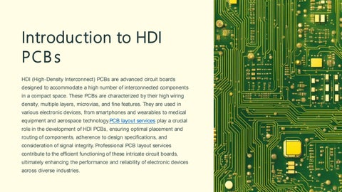
Introduction to HDI PCB s HDI (High-Density Interconnect) PCBs are advanced circuit boards designed to accommodate a high number of interconnected components in a compact space. These PCBs are characterized by their high wiring density, multiple layers, microvias, and fine features. They are used in various electronic devices, from smartphones and wearables to medical
equipment and aerospace technology.PCB layout services play a crucial role in the development of HDI PCBs, ensuring optimal placement and
routing of components, adherence to design specifications, and consideration of signal integrity. Professional PCB layout services contribute to the efficient functioning of these intricate circuit boards, ultimately enhancing the performance and reliability of electronic devices across diverse industries.