
2600/2600 A . VCS DOMESTIC (MIN) Field Service , Manual F01DDl33 Rev. 02
ATARI, INC.
Consumer ProductServices 345 W. MaudeAvenue
Sunnyvale, CA 94041
Q•_c-.c.._c:-o-.
PART TITLE
NO. OOZI
ENGINEERINGCHANGEREQUEST
2600/2600A VCS DOMESTIC FSM Error in Flowcharts and Parts Lists
DESCRIPTION OF CHANGE:
Replace pages 4-25, 6-21, 8-3 and 8-7 with the attached corrected pages.
Replace cover page with new (Rev. 02) co ver page.
Retain this ECN as a record of these changes.
ENGINEERING CHANGE REQUESTER-PLEASE COMPLETE ABOVE DOTTED L.INE················

REASON FOR CHANGE DENIAL OR COMMENTS: �O
ENGINEERINGCHANGENOTICE
WHEN SIGNATURES AND E.C.N. NO. ARE PRESENT THIS E.C.N.NO. 0021 E.C. R. BECOMES AN E.C.N.
E.C.R.
Latest
-
DATE 1-2]-83 REQUESTER S. Doyle REASON FOR CHANGE REQUEST: PARTNO. FDI00l33
REV. 02 �---------------------------
D
ATE

A T A RI V IDE 0 COM PUT E R S Y S T E MTM FI ELD SERVI CE MANU AL MODEL 2600/2600A DOMESTIC (M IN)
Atari believes that the information described in this manual is accurate and reliable, and much care has been taken in its preparation. However, no responsibility, financial or otherwise, shall be accepted for any consequences arising out of the use of this material. Information contained herein is subject to change. Revisions may be issued to advise of such changes and/or additions.

2600/2600A Domestic YCS
Correspondence regarding this document should be forwarded to Manager of Technical Support, Consumer Product Service, Atari, Incorporated, 845 W. Maude Sunnyvale, California94086.
Table of Contents

Title
INTRODUCTION
THEORY OF OPERATION
2600A Model Differences - All Revisions

2600A Model Differences -Revisions 14 and 15
2600A Model Differences - Revisions 16 and up Summary
SCHEMATICS AND SILKSCREENS
TESTING AND TROUBLESHOOTING Equipment Requirements Test Procedures and Methods
Test
Section 2 3 5 6 7 8
Introduction Overview
Game Console Outer Casting Switchboard Motherboard
lnitialization RAM Test Color Bar Test Gray Bar Test Diagnostic Matrix Test Audio Tones Test Paddle Control Lines Test 2600 DIAGNOSTIC FLOWCHART SYMPTOM CHECKLIST 2600 Symptom Checklist 2600A Symptom Checklist 2600A DIAGNOSTIC FLOWCHART GAME CONTROLLERS Overview Joystick(X-Y) Controller Joystick(X-Y) Controller Check Paddle Controller PaddleControllerCheck Driving Controller Driving Controller Check Keyboard Controller Keyboard Controller Check ATARI CX2600 (MIN) PARTS LIST ATARI CX2600A (MIN) PARTS LIST vii 1-1 1-1 1-1 1-2 1-2 1-3 1-4 1-5 1-6 1-6 1-7 2-1 3-1 3-1 3-2 3-2 3-6 3-7 3-7 3-8 3-9 3-10 3-11 3-13 3-14 4-1 5-1 5-2 5-5 6-1 7-1 7-1 7-1 7-3 7-4 7-5 7-6 7-7 7-8 7-10 8-1 8-5 iii 2600/2600A Domestic VCS
2600 Model Modifications 2600A Model Modifications Testingwith the Diagnostic
Cartridge (Version 2.6)
Table of Contents


SERVICE BULLETINS
List of Wustrations
Title
2600 Functional Diagram
2600 Game Console
2600 Switchboard and Motherboard Assembly
TVSwitchbox
2600A Game Console
2600A Board Layout
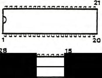
2600/2600A IC Pinouts
2600 Motherboard Silkscreen
2600 Channel 3 Switchboard Silkscreen
2600 Channel 3 Switchboard Schematic
2600 Channel 2-3 Switchboard Silkscreen
2600 Channel 2-3 Switchboard Schematic
2600A Motherboard Silkscreen (Revs. 1-13)
2600A Motherboard Silkscreen (Revs. 14 and 15)
2600A Motherboard Silkscreen (Revs. 16 and up)
InsertedinFront Pocketof Notebook:
2600 Motherboard Schematic
2600A Motherboard Schematic (Revs. 1-13)
2600A Motherboard Schematic (Revs. 14 and 15)
2600A Motherboard Schematic (Revs. 16 and up)
2600 Trigger Circuitry with Static Modification
2600 Static Modification Zener Diode
Location of Colored Dot Over Trace
2600 Switchboard Static Modification
2600A (Revs. 1-13) Static Modifications
Switch Initialization Positions
Defective RAM Patterns
Color Bars Screen
Gray Bars Screen

Diagnostic Matrix Screen (Shorting Plugs OUT)
Diagnostic Matrix Screen (Shorting Plugs IN)
Audio Tone Test Screens
Section 9 Figure 1-1 1-2 1-3 1-4 1-5 1-6 2-1 2-2 2-3 2-4 2-5 2-6 2-7 2-8 2-9 3-1 3-2 3-3 3-4 3-5 3-6 3-7 3-8 3-9 3-10 3-11 3-12
9-1 1-1 1-2 1-3 1-4 1-5 1-6 2-3 2-4 2-6 2-7 2-8 2-9 2-10 2-11 2-12 3-3 3-4 3-4 3-5 3-6 3-7 3-8 3-9 3-10 3-11 3-12 3-13 iv
VCS
2600/2600A Domestic
List of Illustrations(Continued)


Switch Initialization Positions
Color Bars Screen
Defective RAM Patterns
Gray Bars Screen
Defective Gray Bars Screen
Diagnostic Matrix Screen (Shorting Plugs OUT)
Diagnostic Matrix Screen (Shorting Plugs IN)
Diagnostic Matrix Screen with Defective Pattern
Audio Tone Test Screens
RC Waveforms
STC Address Line Waveforms


STC Data Line Waveforms
Joystick (X-Y) Controller
Joystick (X-Y) Schematic
Paddle Controller
Paddle Controller Schematic
Driving Controller
Driving Controller Schematic
KeyboardController
Keyboard Wiring Diagram
4-1 Figure 4-1 4-2 4-3 4-4 4-5 4-6 4-7 4-8 4-9 4-1 0 4-1 1 4-12 7-1 7-2 7-3 7-4 7-5 7-6 7-7 7-8 7-9
Title
Keyboard
List of Tables Title Connected Pins on YCS Motherboard Page 4-35 4-36 4-37 4-38 4-39 4-40 4-41 4-42 4-43 4-44 4-46 4-46 7-1 7-2 7-4 7-5 7-6 7-7 7-8 7-9 7-9 4-47 v 2600/2600A Domestic YCS
Schematic
INTRODUCTION
The Video Computer System™ (YCS) Field Service Manual is organized in nine sections:
• THEORY OF OPERATION - overview of how the YCS works and what the basic assemblies look like.
• SILKSCREENS AND SCHEMATICS - electrical drawings and layouts of the printed circuit boards.
• TESTING AND TROUBLESHOOTING - overview of the procedures for testingand repairing the YCS unit.
• 2600 DIAGNOSTIC FLOWCHART - thorough flowchart enabling the technician to test and trou�leshoot a defective 2600 unit.
• SYMPTOM CHECKLIST - for the experienced technician, a list of the high failure parts and the flowchart entry point for that particular problem.
• 2600A DIAGNOSTIC FLOWCHART - thorough flowchart enabling the technician to test and troubleshoot a defective 2600A unit.
• GAME CONTROLLERS - overview of hand controller construction with electrical schematics and recommended test and repair procedures.
• PARTS LIST - detailed breakdown of all parts used in both the 2600 and 2600A .
• SERVICE BULLETINS - section to be used to hold service bulletins released by the Manager of Technical Support. These bulletins will include changes in recommended repair procedures and required modifications for units in the field.
The manual is designed for use by both experienced and inexperienced service personnel. The Diagnostic Flowcharts (Sections 4. and 6) provide detailed diagnostic and repair procedures for technicians who are not yet completely familiar with the YCS. The Symptom Checklist (Section 5) provides a fast repair reference for the more experienced technician.
vii 2600/2600A Domestic YCS
SECTION I
THEORY OF OPERAnON
INTRODUCTION
There are currently four types of ATARI Yideo Computer Sy.stems. The original model (2600) is composed of two PC Boards connected by a l2-pin ribbon cable with the motherboard surrounded by a heavy aluminum casting.
The other models (2600A: Revisions 1-13, Revisions 14-15, and Revisions 16 and up) are composed of a single board with a light aluminum shield. The single board models differ slightly in the video output circuitry. Component differences are:
• Revisions 1-13 have no diodes on TIA lines L�l and Sync.
• Revisions 14-15 have diodes and pull-up resistors on TIA lines LMI and Sync.
• Revisions 16 and up include the above mentioned diodes and resistors as well as a timer chip.

The revision level is etched directly on the PC board.
OVERVIEW
The ATARI Yideo Computer System (YCS) Models 2600/2600A are state-of-the-art microcomputers. They receive instructions for the operation of different games from individual Read-Only-Memory game cartridges and interpret data from the players hand-held controllers. They also allow game players to select both a specific version of each game and the player difficulty (on a per player basis). Figure 1-1 is a block diagram of the functional flow of the YCS Model 2600. Section 7 describes the player controllers•.
..-,. VIM.... (A.r_"-ter. 110'lAC r-------, I :.!��. I I I "..D I c-- I I I
1-1 2600/2600A Domestic YCS
Figure 1-1. 2600 Functional Diagram
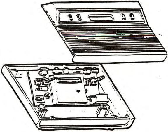
GAME CONSOLE
The YCS game console is composed of an outercasting that houses the switchboard and the RF radiation shielded motherboard.
Outer Casting

The casting consists of three pieces of plastic (see Figure 1-2). The pieces include the base, which holds the switchboard and motherboard assembly; the top; and the bezel.
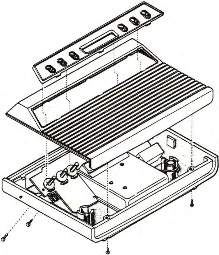 Figure 1-2. 2600 Game Console 1-2
2600/2600A Domestic YCS
Figure 1-2. 2600 Game Console 1-2
2600/2600A Domestic YCS
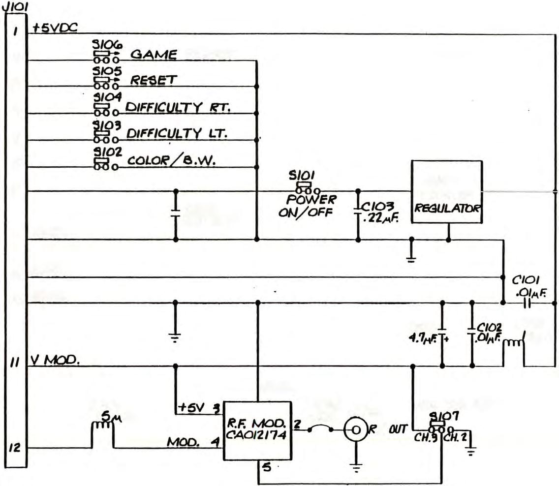
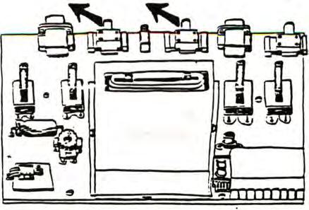
Switchboard
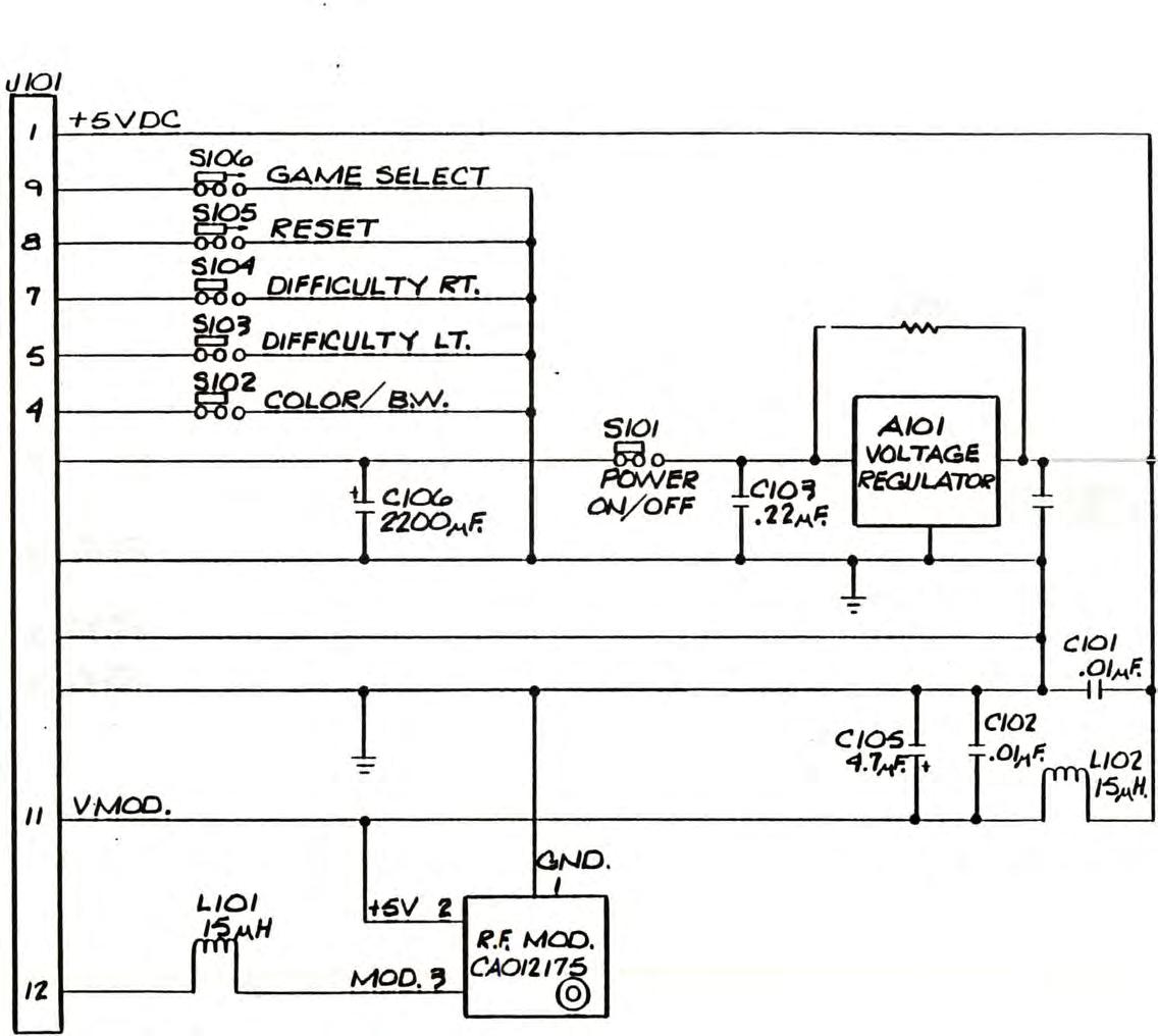
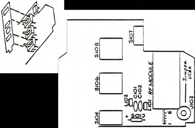
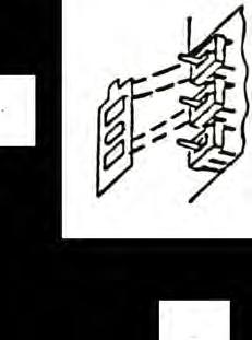
The switchboard assembly holds the player option switches, the power supply, and the RF modulator (See Figure 1-3).
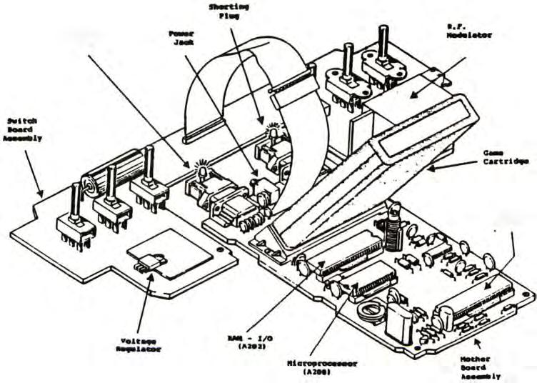
• PLAYER OPTION SWITCHES
Switches S101 thru S104 are double-pole, single-throw. Switches S105 and S106 are double-pole, double-throw. AU switches are connected between the switchboard and the motherboard by 12-conductor flexible ribbon cable.
• POWER SUPPLY
The power supply is composed of a +5 voltage re�ulator, filter capacitors, and the power on/off switch. Unregulated DC is supplied to the board from the battery eliminator. A suoply of +5 volts is routed through a filter circuit to the RF modulator. The motherboard also receives its power (+5 volts Vce) from the switchboard via the same l2-conductor ribbon cable referenced above.
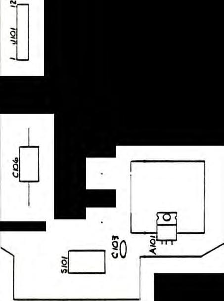
• RF \,10DULATOR

The RF modulator. converts the signal received from the Television Interface Adaptor chip on the motherboard to a frequency that a television can receive and interpret. Data between the RF module and the Television Interface Adaptor chip is passed via the 12-conductor ribbon cable which connects the motherboard to the switchboard. A coaxial cable passes this signal from the RF module to the switch box mounted on the back of the television.
-... 'I.. "1. ,aall
2600/2600A Domestic VCS
Figure 1-3. 2600 Switchboard and Motherboard Assembly 1-3
\1otherboard
The motherboard is composed of a PC board containinga microprocessor (MPU) chip, a combination Random Access Memory - Input/Output (RAM-I/O) chip, and a Television Interface Adaptor (TIA) chip (see Figure l-3). The board also contains numerous capacitors, resistors, transistors, and other assorted electronic components. These parts are all listed in Section 8, PARTS LIST.
• MICROPROCESSOR CHIP
The heart of the VCS is the 6507 microprocessor chip (MPU). This device makes decisions for the VCS based upon information it receives from the game cartridge and the RAM-I/O(discussed in the next paragraph).
• RANDOM ACCESS MEMORY-INPUT/OUTPUT CHIP
Temporary storage of data from the MPU is provided by the 6532 Random Access Memory-Input/Output (RAM-I/O) chip. This chip also scans the option switches and the joystick I/O lines for information and maintains time accounting for the MPU.
• TELEVISION INTERFACE ADAPTOR CHIP
This ATARI proprietary chip generates audio and video signals which are required by the RF modulator. The Televi�ion Interface Adaptor (TIA) chip also contains the analog-to-digital converter circuitry that allows the MPU to understand signals originating in the hand-held paddle controllers.
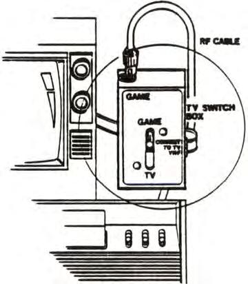
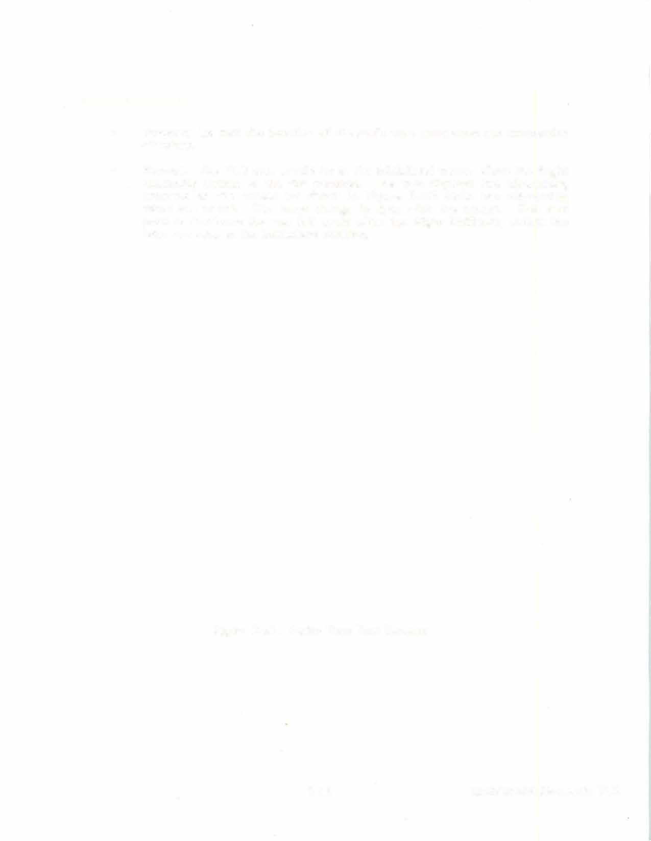
TIA outputs are processed by additional circuitry into a composite video, sound, and color signal which is routed to the RF module on the switch,.. board via the 12-conductor ribbon cable. The RF module converts the composite signal to a RF signal acceptabl� to the television. A coaxial cable transmits this RF signal from the console to a selection box that can be mounted on the T.V. This switchbox (Figure 1-4) allows you to display either a signal received by the antenna (for normal T.V. viewing) or a signal from the VCS (for playinga game).
l-4 2600/2600A Domestic VCS
Figure 1-4. TV Switchbox
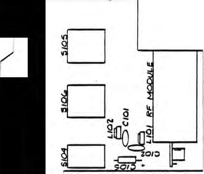
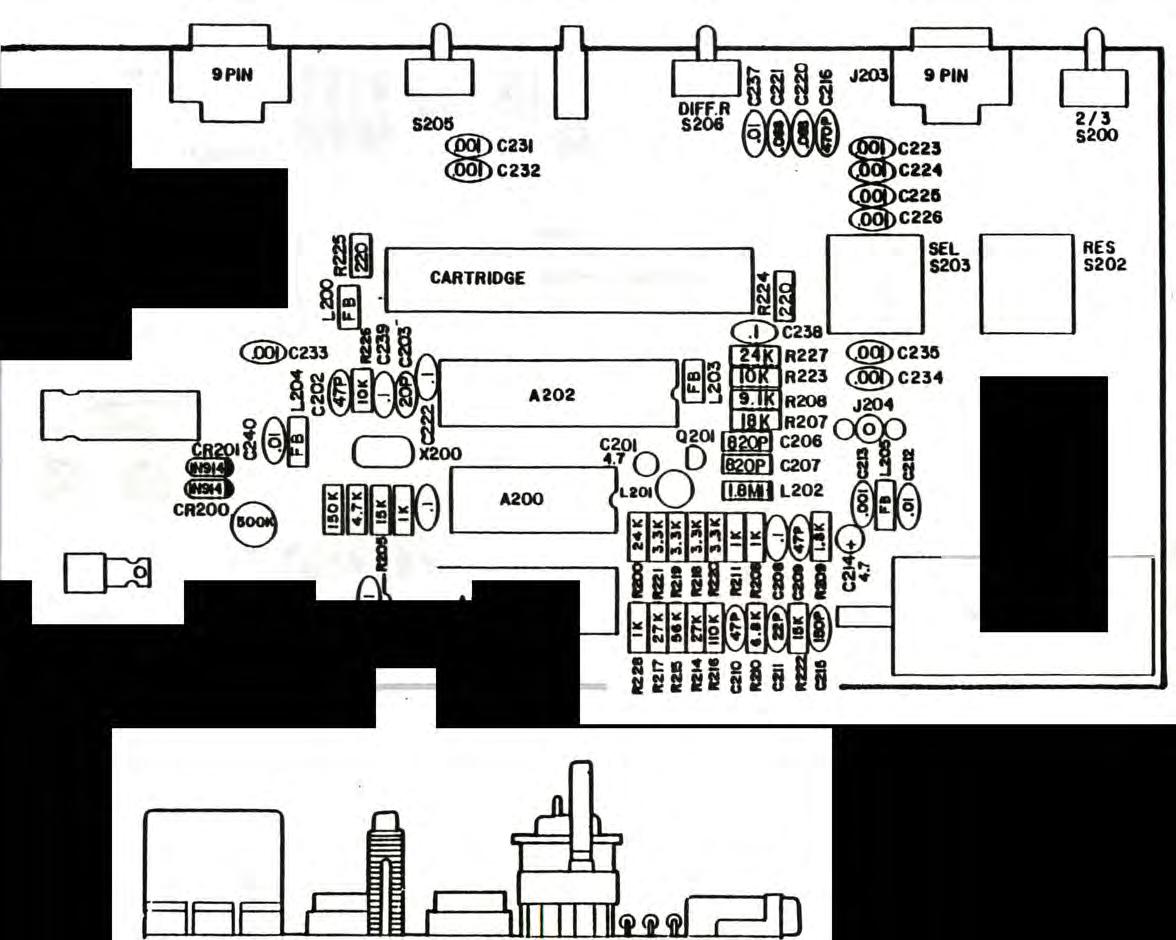
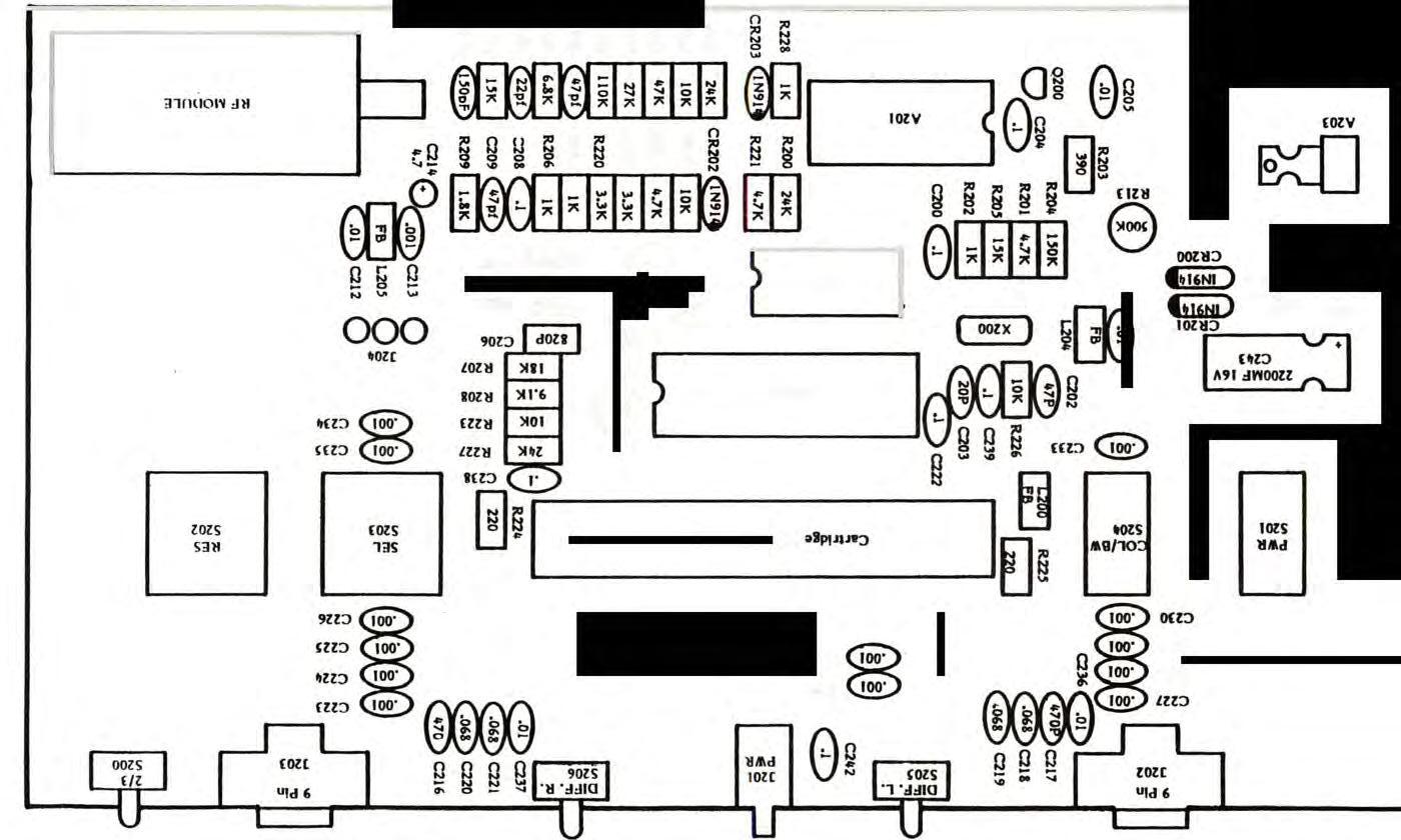
2600A MODEL DIFFERENCES - ALL REVISIONS

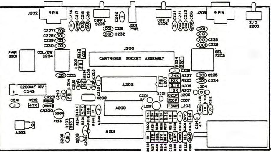
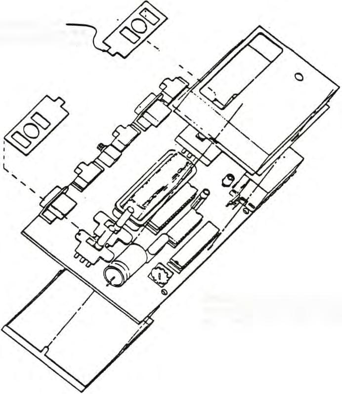
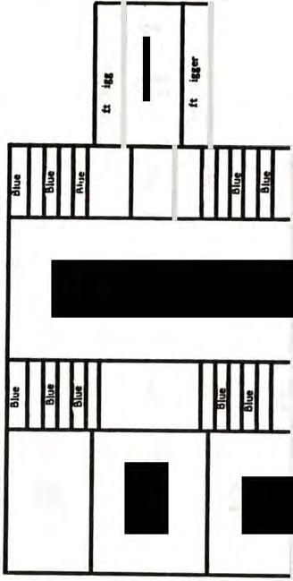
The major difference between the newer single board YCS (2600A) and the original YCS (2600) is that all of the components formerly on the switchboard are now located on the motherboard (See Figure 1-5). This includes the player control function switches (Power ON/OFF, COLOR/BW, GAME SELECT and GAME RESET), RF modulator and power supply circuitry. The single board design eliminates the need for the ribbon cable, which connected the switchboard to the motherboard on the 2600 YCS.
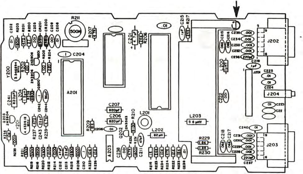
Gone, too, are the luminescence and RF output buffers and the two TIA input buffers, all of which were contained in chip A203. In the oscillator circuit, one of the transistors and its associated network has been eliminated and R227-R230 (paddle control lines) are no longer present. C239, going to pin 7 on J202 and J203, has been replaced by C236 and C237 (See Figure 1-6).
1-5 2600/2600A Domestic YCS
Figure 1-5. 2600A Game Console
In addition to the component changes, the physical location of several parts has also been changed. Instead of having the right and left difficulty switches placed on top of the game, they are located at the rear of the console next to the game controller plugs. The channel selector switch is also located at the rear of the console. The game cartridge socket is no longer angled, but is mounted verticallyon the board.
2600AMODEL DIFFERENCES-REVISIONS 14 AND 15

Revisions 14 and 15 contain the model differences described above, and in addition have new components on the TIA lines, LMl and Sync. There are two IN9l4 diodes to prevent feedback on the lines and two additional pull-up resistors to insure the signal is at +5v. To compensate for any signal loss, R2l5 and 217 have been changed to 47K (R215) and 24K (R2l7).
2600A MODEL DIFFERENCES-REVISIONS 16 AND UP
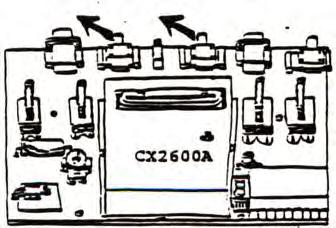
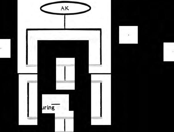
Revisions 16 and up contain the model differences described above; theyalso include a timer chip (A205) added to the reset circuitryof the MPU chip. This chip eliminates the problem of power-on reset failures. 2600/2600A

C225 C224 001CZ25 00 C22S ,,-�---, i\l;.D:g, RFMOD
Figure 1-6. 2600A Board Layout (Revs 1-13)
Domestic yeS
SUMMARY

The yeS is a microcomputer that receives its operational instructions from game cartridges, the game console, and player controllers. The 2600 switchboard and motherboard assemblies are housed within an outer casting and are the principle assemblies addressed in the remainder of this manual. The boards are connected by a 12-conductor ribbon cable which passes not only power, but also data between the two boards.
Three chips of the motherboard allow for the interaction between the game and the player. These chips are the microprocessor (MPU), the Random Access MemoryInput/Output (RAM I/O), and the Television Interface Adapter(TIA) chips.
The 2600A model differs primarily in the location of the components formerly located on the switchboard. They are attached directly to the motherboard and eliminate the need for the switchboard and the ribbon cable. The 2600A Revisions 14- and up include even further additional components to improve the performance of the output circuitry.
1-7 2600/2600A Domestic Ves
SECTION 2

SILKSCREENS AND SCHEMATICS
On the following pages are representative silkscreens and switchboard schematics for the ATARI Video Computer System. The motherboard schematics for all 2600/2600A VCS models are located in the pocket at the front of this binder. Minor variations in design maybe encountered depending on the production date of the game, but these schematics provide all details required for an in-depth understanding of all 2600 units, including the various 2600A model revisions•.

2-1 2600/2600A Domestic VCS

NOTES 2-2 2600/2600A Domestic yeS

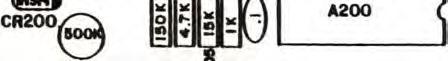
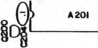
o VOLTAGERECULATOR (Top Vie'N) Ingndout 40 '-pinv�sion (o,annel 2 or3) 3-pinversion (o,anne1 2 or3) -.w .. 20 t:�::::::::J 1 1D�'�'�" 9 w... ...... .. 1 a Pin1",,11I1Pin iii Pinl� jPin I Cathode -a 14 I RF�ad. RF�ad. >- Anade 1I I .'JAT.
A201 andA202 (TopView) A200 (TopView) A20)
Diode
L.'vI3"'O T.l.7&MO",C
(TopView) RFMadulator (TopView) RFMadulator (TopView)
2600/2600A
VCS
Figure 2-1. 2600/2600A IC Pinouts
2-3
Domestic

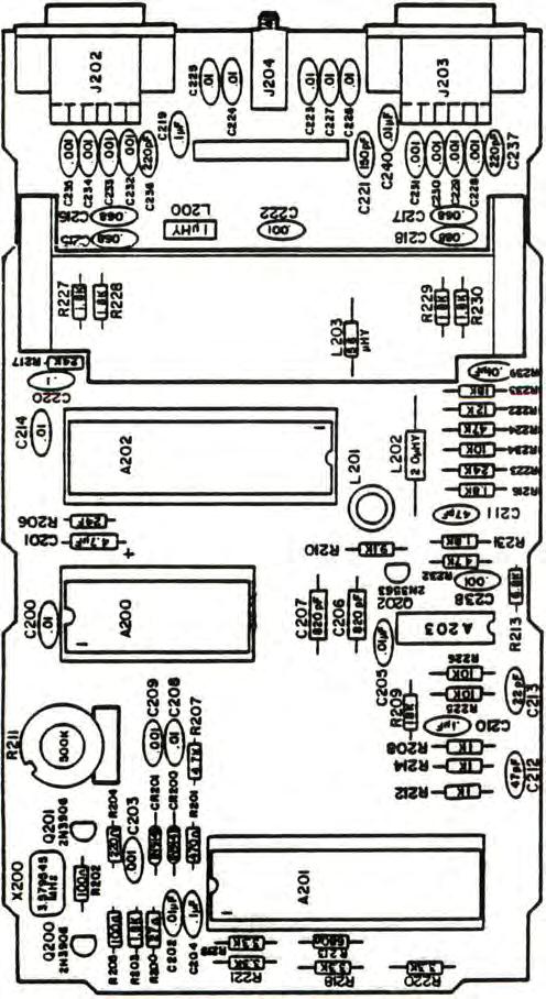
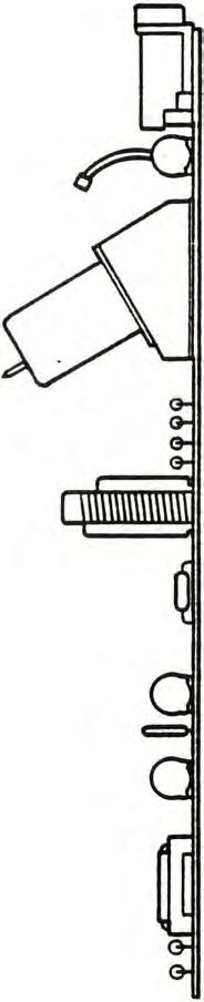
 Figure 2-2. 2600 Motherboard Silkscreen 2-4
2600/2600A Domestic ves
Figure 2-2. 2600 Motherboard Silkscreen 2-4
2600/2600A Domestic ves
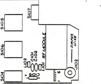
The following variations mayappear on the 2600 switchboard:
CHANNEL 3SWITCHBOARD:
CI02 mayor maynot be in pJace.
CI03and/or CI04- mayor maynot be in place.
CI03and/or CI04- maybe mylar dipped .22 ufo
CI03and/or CI04- maybe ceramic .Oluf (See Figures 2-3and 2-4-).
CHANNEL 2 OR 3 SWITCHBOARD:
The holes on the PC board for the GAME RESET and GAME SELECT switches maynot be wide enough apart for the switch legs. To correct this the legs of the switch must be bent in so theyfit into the holes (See Figures 2-5 and 2-6).
2-5 2600/2600A Domestic YCS
o
2-6
Figure 2-3. 2600 Channel 3 Switchboard Silkscreen
VCS
2600/2600A Domestic

N I '-I N 0'\ o oN 0'\ o o ):CJ o 3 !l VI .... .-' n < n VI '11 .-' OQ C .., !l N I � Vol l/l � ::t' n :r 0o III .., 0. W :r !l 3 III ... .-' n tllOl �t----� 4r-----�������--� 2 ______ ___ .�--.--�-I ,aND. "GND. 10 GkJD. �IOI CI04 .22/-iF.


o
2-8
Domestic
Figure 2-5. 2600 Channel 2-3 Switchboard Silkscreen
2600/2600A
yeS

N I \D N 0\ o oN 0\ o o » � 3 � VI '. r+ ...... () < () VI N 0\ o o () :T C\l :J :J �N I Vo) VI � ...... r+ () ::r CT o C\l ., a. VI () :T � 3 C\l r+ n' q SELECT 8 ET 1 tn". � LT. 4 2 AIDI VOLTAGE + em =JGND. tOO""F. ffEt3ULA" GND.10GND. CI05 1I ________ ______ ____________ GflO. LIOI IH. +5V MOD. -5. �R.t.lIOZ CII.SELeCT 7 .F.OUT··............. CH, L.IOZ �H.


N I o N � o oN 0\ o o » CJ o 3 � VI .-+ n' < () Vl 'TI Oil' c ., � N I '" N 0\ a a » s: o .-+ :T � ., c::r o III ., 0. Ul �. 0" � ., (I � :J J202 ft�nR DIFF.L ge C22116W S20®C231 i!3�. C228 �C23Z CZ29 . C230 . .lZOO =DaL/.�D CARTR� SOCMn ASSD&Y .�MF�A -2 02 + CZ43 C241 RZIZ 0)(200 ____ CDlml CR200e 5 ; � -: _A2_00_ RIll 2�I� 11____ �@M _ A _ 20 _1 l-L...&-�'>oJ�'� A203 RFMOD


_ N '"' '" N N U U � � N N U U >-1!<.... . � £OZ1GJ N2< ... N N0 2 u � �rn § O ®� u .. I< 0 .0 N � a.:....-... .. �0 N • U � lin! atn! 61Z:1I 6UlI�IO ZZ:Z:'lI ITO OT,1I OTO 9TZ:1I ilTZ1I 'Tn! OEZ'lI • .:TZlI Fi gure 2-8. 2600A Motherboard Silks creen (Revs . l4and 15) 2-11 2600/2600A Domesti c ves


N I N N (]'\ o oN (]'\ o o >o o 3 � VI rl ...... () < () VI ." oti· c .., � N I � . N (]'\ o o >� o rl ::T � ., cO PI ., 0. VI ...... � � ., � � :J � 0. C "0J202 �t " !! &;J 5205 J201 520. C227 .001 �e'?3' C228 .001 001 C232 C223 C2Z!3 (@ 10 Cl C2c;"'4 JZOO 5Z00 o J204
SECTION 3
TESTING AND TROUBLESHOOTING
EQUIPMENT REQUIREMENTS
You require eight basic pieces of equipment in order to analyze failures in the 2600/2600A Video Computer Systems (VCS). These items include:
• A15 MHz oscilloscope
• A Video Computer System switchboard assembly that is known to be operating properly (not required for repairing 2600A units)
• A Video Computer System diagnostic test cartridge, version 2.6 (DTC)
• Two blue controller port shorting plugs for use with the 2.6 (DTC) diagnostic cartridge
• Signal Tracing Cartridge (STC or KLUGE)
• VCS Field Service Manual for Domestic \!lodel 2600/2600A
• Color television set (properly adjusted)
• Frequency Counter
3-1 2600/2600A Domestic VCS
TEST PROCEDURES AND METHODS
Atari requires each 2600/2600A model returned for service to be checked for certain conditions. In some instances, a unit must be modified to conform to Atari standards. These changes are summarized below.
2600 MODEL MODIFICAnONS
• Each 2600 model opened must be modified as shown in FiI;�ure 3-1 to provide additional protection from static discharge.· A Zener diode is connected between the tri�ger lines and ground, and static strips are placed on the switches on the switchboard (See Figures 3-1, 3-2 and 3-4). These modifications are crucial to preventcomponent damage due to static disCharge.
• Each connector and plug should be checked for a tight, secure fit. Intermittent failures frequently result from a loose connector or plug.
• Connectors 1202 and J203 should be checked for pushed or broken pins.
• If the unit has a green J200 connector, insert cartridge and wiggle it. If the unit shows intermittent problems, replace J200.
• Each board with Molex chip sockets with insertion aids should have the insertion aids removed and the chip reinserted.
• Check that all components (especially those on the perimeter of the motherboard) are properly soldered. Check for broken or shorted trace lines.
• Check for an inductor and capacitor over C20l and R206. Cut the inductor and cap out, being careful not to cut the C201 or R206 leads.
• If unit has a standup regulator and heatsink, inspect for hairline fractures between the regulator and switchboard. Also ensure that the regulator is firmly secured to the heatsink by a Tinnerman clip or rivet.
• Ensure that motherboards (Rev. 8 or lower) have a colored dot over the trace on the upper-left corner of the board. This prevents shorting the board and the casting (See Figure 3-3).
• Two types of 12-conductor cable assemblies have been used on 2600 model units, the flat-wire type and the ribbon type. When a defect is found in the flat-wire type cable assembly or its male connector on the switchboard, the flat-wire cable assembly should be replaced with the ribbon cable assembly and the 12-pin male switchboard connector should be replaced with the 12-pin female switchboard socket.
3-2 2600/2600A Domestic VCS
Install the static modification on all 2600 units. Install CR202 nd CR203 by removing C236 and C237 and inserting the C236/CR202 and C237/CR203 assemblies in their place (See Figure 3-2). CAUTION: Observe the polarity on CR202 and CR203 (the dark band must be toward the J202/J203 connectors). On the switchboard, install the static strips as shown in Figure 3-4.


I.' :=! I:Ie : = ::::::aa:::•• '" o .. C 101 I--��------��---+--------� .
figure 3-1. 2600 Trigger Circuitry with Static Modification
3-3
2600/2600A Domestic YCS


�------W�A.P
I fURN65OLO€R •
CRZOZ,CRZO'5 � (41COl41CO-0"5)
LEADS
C214 GD C200 01 A200 A202 A227 -i1ID� A228 L203 1",...,� 01 , �C2Z3 It .01 cue C1I1<S>
Figure 3-2. 2600 Static Modification Zener Diode
3-4 2600/2600A Domestic YCS
Figure 3-3. Location of Colored Dot Over Trace
+ o o
3-5
Figure 3-4. 2600 Switchboard Static Modification
2600/2600A Domestic yeS
2600A MODEL MODIFICATIONS
• Each 2600A (Revs 1-13) model must have static strips placed on the front panel switches (See Figure 3-5).
• Check each connector and plug for a ti�ht, secure fit. Intermittent failures frequently result from a loose connector or plug.
• Check that all componenets are properly soldered, and check for broken or shorted trace lines.
• If a unit exhibits RF interference that does not clean up usin� normal adjustment methods, or if a series of lines and bri�ht grid distortions on the screen are accompanied by a loud hum even when properly adjusted, a defective or leaking capacitor may be at fault. Replace C24-1 (.1 microfarad) and/or C24-2 (.1 microfarad) located respectively between the power jack and voltage re�ulator•
" " "
.ccc.o'7lI8S�" BaI'CII.�.,.,""".,.",. �IJO0-��SMti.Q
Mount Static Strips onto Front Panel SwitcheS as shown in this drawing.
3-6 2600/2600A Domestic YCS
Figure 3-5. 2600A (Revs. 1-13) Static .\\odifications
TESTING
WITH THE DIAGNOSTIC TEST CARTRIDGE (VERSION 2.6)
The 2600 Diagnostic Test Cartridge (version 2.6 DTC) contains a variety of tests to assist the service technician in identifying the source of problems within the VCS switchboard and motherboard hardware. The test cartridge is used in conjunction with the equipment listed at the beginning of this section. Each test is reviewed in the remainder of this section. Detailed procedures for use of the tests are described in Section 4, 2600 Diagnostic Flowchart, and Section 6, 2600A Diagnostic Flowchart. The tests available in the cartridge are:
• RAM Test
• Color Bar Test
• Gray Bar Test
• Diagnostic \.\atrix Test
• Audio Tones Test
• Paddle Control Lines Test
The technician also has a Signal Trace Cartridge (STC or KLUGE) available for tracking motherboard problems that are not repairable with the Diagnostic Test Cartridge.
INITIALIZAnON
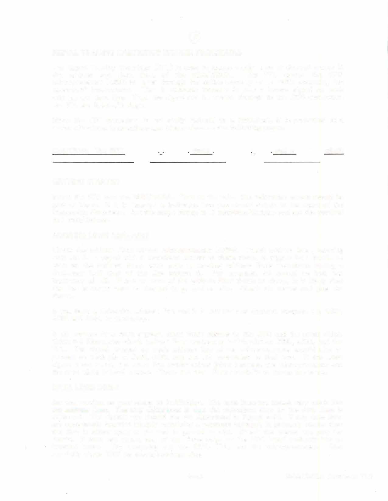
• Purpose: To prepare the VCS unit for testing by the diagnostic cartridge.
• Format: Connect VCS unit to television and battery eliminator. Set television to proper channel (channel 3). Plug in the 2.6 diagnostic cartridge. Set all 2600 switches to the up position. On the 2600A, Set all front panel switches up and rear panel switches to the left (See Fi�ure 3-6).
0GWf � G-toMIP ClPIClA:T"I' UI.«:'T rerr
�: �� �� initially to tn. l.tt
3-7 2600/2500A Domestic VCS
Figure 3-6. Switch Initialization Positions
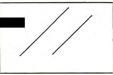
RAM TEST
• Purpose: To test the 6532 RAM chiD for proper operation.
• Format: On power-up the television displays diagonal lines of some type if the RAM is defective. See Figure 3-7 for examples of screens indicating a defective RAM.

NOTE: The absence of defective patterns is no assurance that the entire chipissound, only the RAM. The operation of the I/o and Timer functions is notverified by this test.
/
3-8 2600/2600A Domestic yeS
Figure 3-7. Defective RAM Patterns
COLOR BAR TEST
• Purpose: To test the 6507 microprocessor, 6532 RAM -I/o chip, and TIA chip for correct operation.
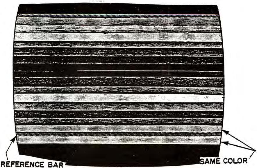
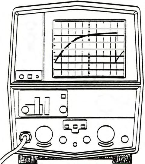
• Format: Set all switches to initialization position. A screen of horizontal color bars is displayed (See Figure 3-8). The screen should be steady and unchanging. A gray or blue horizontal reference line runsacross the screen about three bars from its bottom. This reference line is thinner than the bars around it. R211 (R213 on the 2600A board) should be adjusted so the bars immediately above and below the reference line are within one shade of each other. Proper operation of the unit is indicated by being able to make this adjustment and by consistent color within the entire span of each bar on the screen. Minor glitches on the edges of the color bars are acceptable. Leave this test on for at least ten seconds in order to catch any intermittent problems, such as a bar momentarily changing colors or blanking out.
NOTE: This figureisablackand white representationofacolor television screen.
3-9 2600/2600A Domestic ves
Figure 3-8. Color Bars Screen
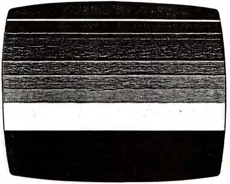
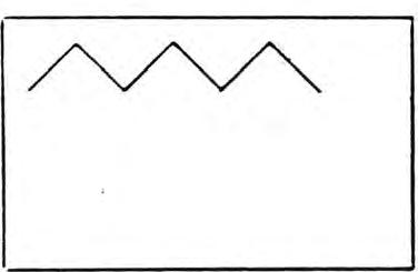
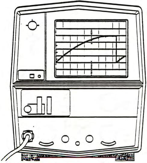
GRAY BAR TEST
• Purpose: To test the function of the luminescence lines (L.\IO,LMl, LM2) from the TIA chip to the RF :Vlodule.
• Format: Move the Color/Black & White switch to the Black and White position. There should be eight horizontal gray bars displayed, going from black at the top to white at the bottom in even gradations (See Figure 3-9). The screen should be steady and unchanging. These llnes may have minor litches on their edges. A thin white line always appears just over the top black) bar. No color should appear anywhere on the screen. The areas above the top (black) bar and below the bottom (white) bar are of no importance to the test. This test should be left on for at least ten seconds to ensure that there is no "flashing" of any color or shifting of the gray bars.


3-10 2600/2600A Domestic VCS
Figure 3-9. Gray Bars Screen
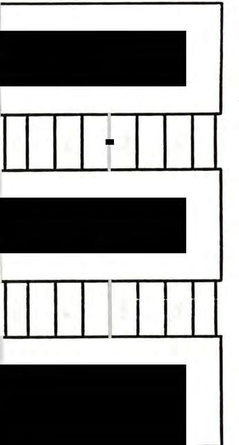
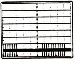
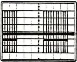
DIAGNOSTIC MATRIX TEST

• Puroose: To test the proper function of the Input-Output ports of the VCS unit.
• Format: Set all switches to the initialized pOSition, then move the Left Difficulty switch to the "B" position. The test is performed in two parts:
1. With the blue shorting plugs removed, the matrix of nine rectangles on the screen should look like Figure 3-10.
2. The shorting plugs are then inserted and the pattern should look like Figure 3-11.
3. Press the GAME SELECT switch. If the switch is properly functioning, that area of the matrix will black out. Release the GAME SELECT switch and repeat the procedure with the GAME RESET switch.
The Matrix jumps once every second.
:: .. .3 ., :: .s Q. 2 '" :: .5 Q.
� :: .5 .s Q. Q. � • .3 ., ., � :: .s .s Q. Q. 2 .. � :: .s .s Q. Q.
I PInk � I� .5 Q. 6HZ � • .! .3 ., ., G<een !:: = .s .s ... Q. 6HZ 1 '" G<een !:: = .5 .s ... Q. ";Z
� ... .. '" .s .s .s Q. Q. Q. � � � .! .. .. '" � � � .s .s .s Q. ... II. 1 '" � .. .. '" '" .s .s .s ... ... ... P1nIc - \I :I Rlsht ;; ;; Trig« ,:: .::: l: • G<eo!ft Nat UMd .. ... ... � � I� � Z �� � .. '" 1 • 1 !I .3 ;; .. .. .. G<_ PI,* or G<eenNat UMd NatUwd .I � 1 � � 1 ., .. ., 1 .I !I ! '" .. iii G<ftft e..... e..... e..... G<een ReletSelectRe.tNat Used SwitchSwitchSwitch
3-11 2600/2600A Domestic YCS
Figure 3-10. Diagnostic Matrix Screen (Shorting Plugs OUT)
I Gr�en Creen :: !. :: � I� � .. .. 0 0 .: .s .: .s .s .s .s "- "- "- "- "- "- "6}2 • Ii NotUsed :I RIsI't .; Not Used ;E Trlger ,: :I j j G<een NotUsed ... .. -lI 1 � .I � .. u � � � � .! ::;; .., iii .., OJ OJ OJ OJ ! !! .3 .. �11 iii .., .3 .., .., J 1 J .I .., <II G<een G<een 2 .. :: !. :: � = .. 0 0 .s .s c .s .s .s .s .s ""- a: "- "- "- "- "PInk«G<.... NotU.... NotUsed "2 � � 1 1 � ::;; iii OJ .., .. .. � .I � . �� .., .I J ! .I <II .. os OJ G<_ G<.... :: !. :: � = � . :I 0 .s .s .s .s .s Ji .s .s "- "- "- "- Go ... ... ... Ca_ ea- eaR_t 5e1ect Retet Switch Switch Switch G<.... NotllMd "i2
3-12 2600/2600A Domestic yeS
Figure 3-11. Diagnostic Matrix Screen (Shorting Plugs IN)
AUDIO TONES TEST
• Purpose: To test the function of the audio tone generation and modulation circuitry.

• Format: The yeS unit should be in the initialized mode. Move the Right Difficulty switch to the "B" position. The test displays two alternating patterns on the screen (as shown in Figure 3-12) while two alternating tones are heard. The tones change in sync with the screen. This test pattern continues for one full cycle after the Right Difficulty switch has been returned to the initialized position.
3-13 2600/2600A Domestic yeS
Figure 3-12. Audio Tone Test Screens
PADDLE CONTROL LINES TEST
• Purpose: To test the proper operation of the Paddle Control Lines by viewing the analog waveforms at the analog-to-digital conversion inputs of the TlA chip.


• Format: Pins 37, 38, 39, and 40 of the TlA chip are checked with the oscilloscope with the YCS unit in Diagnostic Matrix mode and with the shorting plugs in place. This test is required only if there is a problem with the hand controller lines. The procedure for this test is detailed in Section 4.
3-14 2600/2600A Domestic YCS
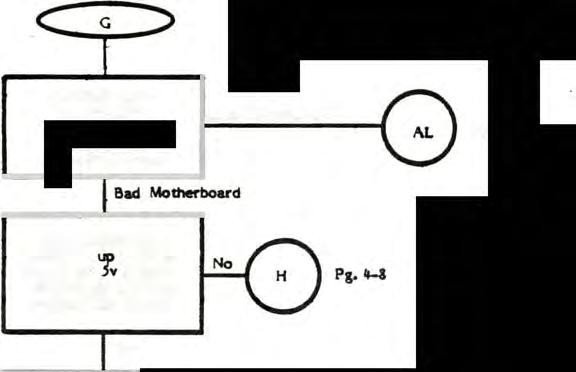
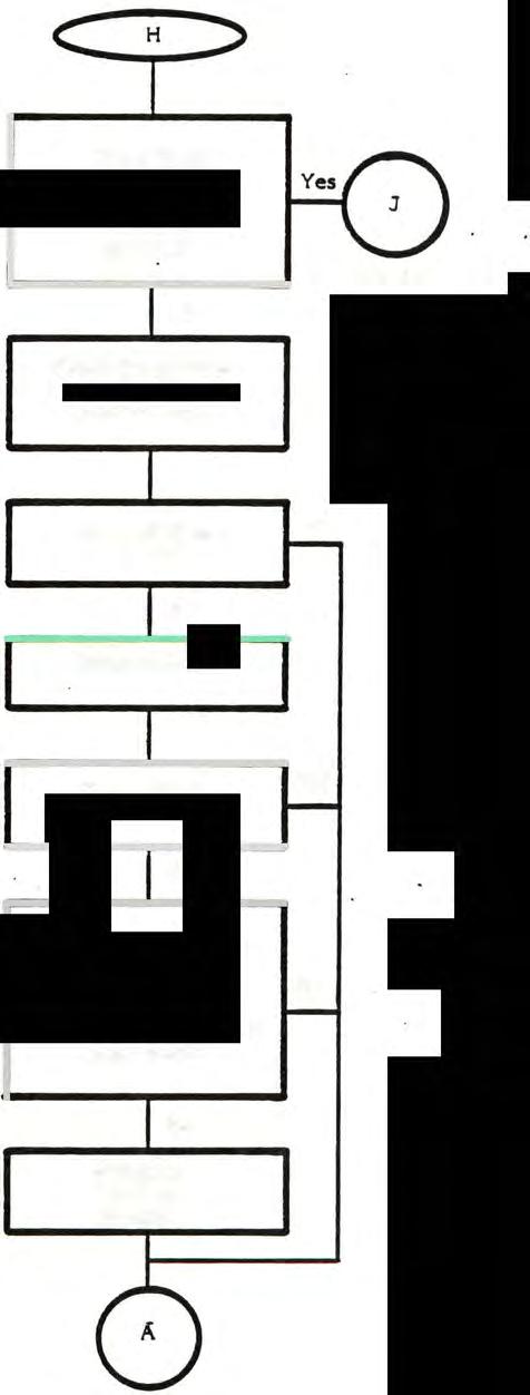
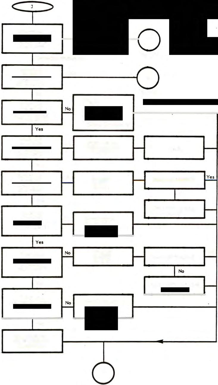
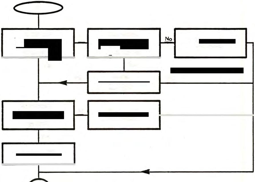
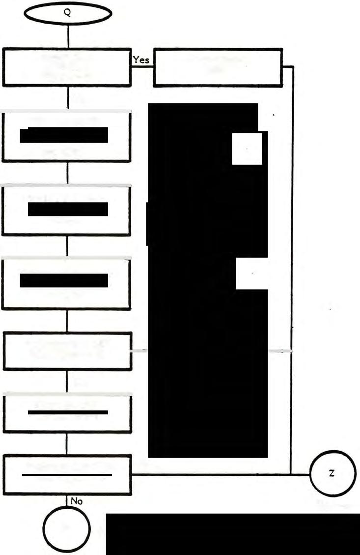
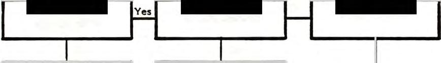
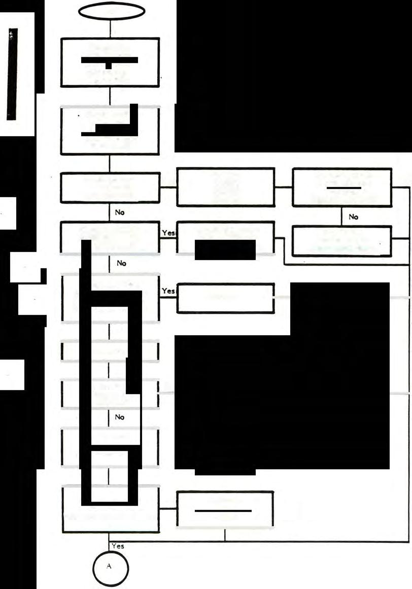
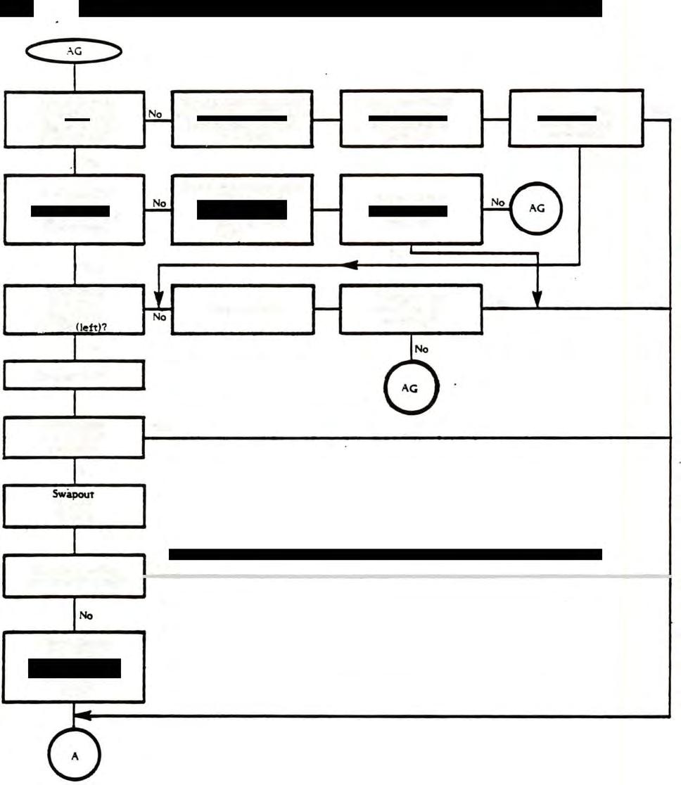
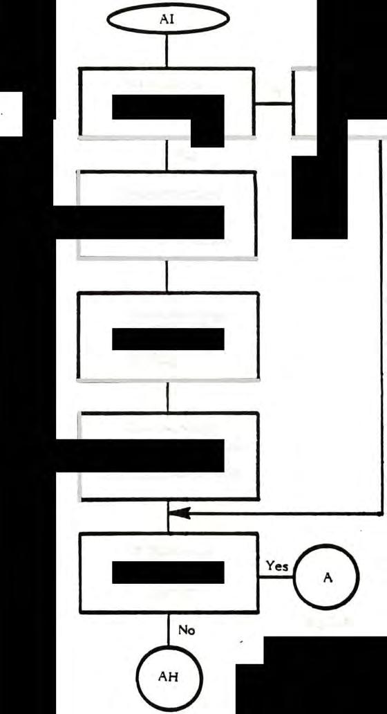
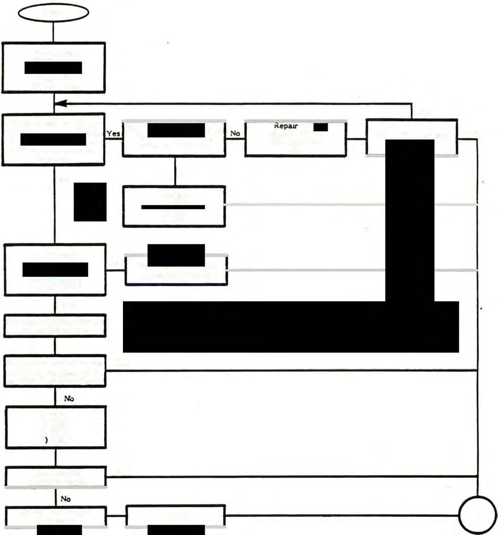
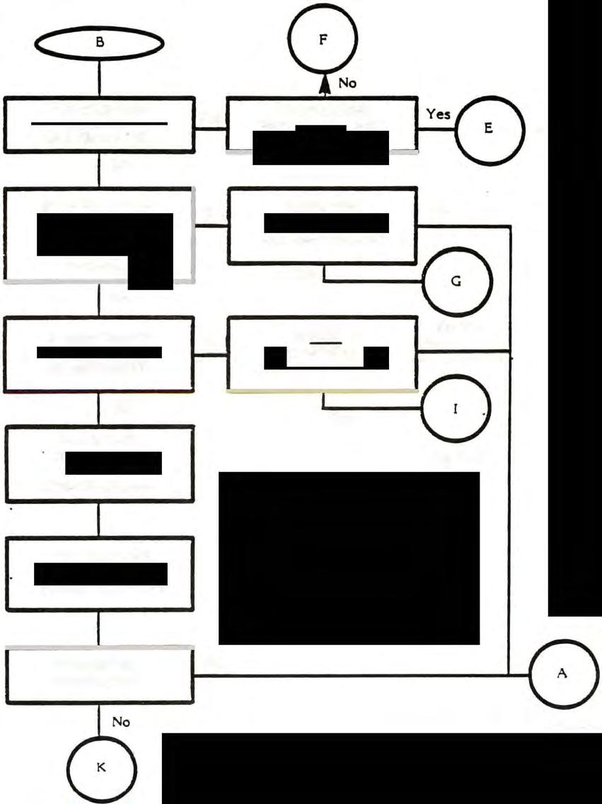
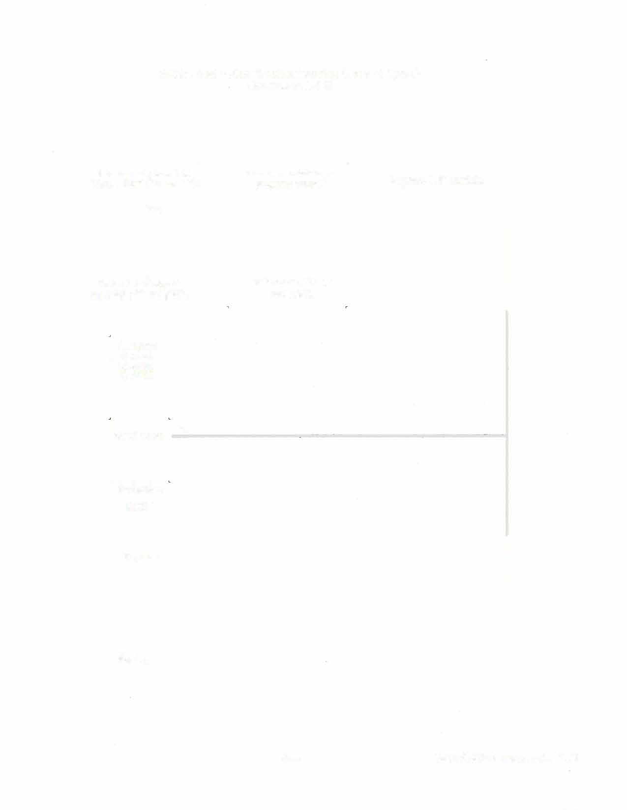
2600 DIAGNOSTIC FLOWCHART
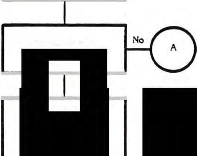
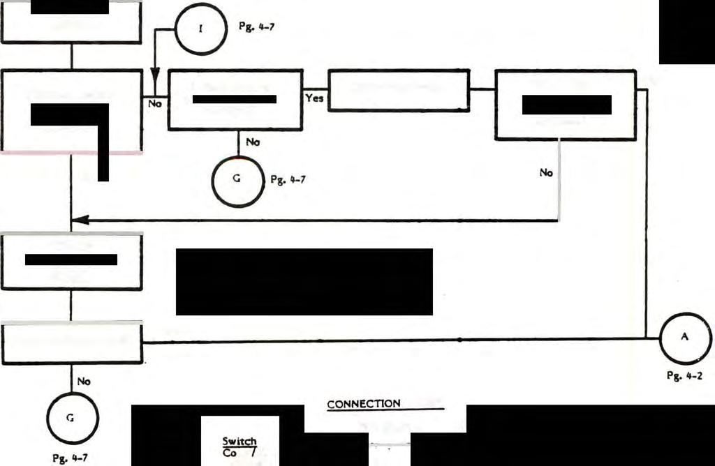
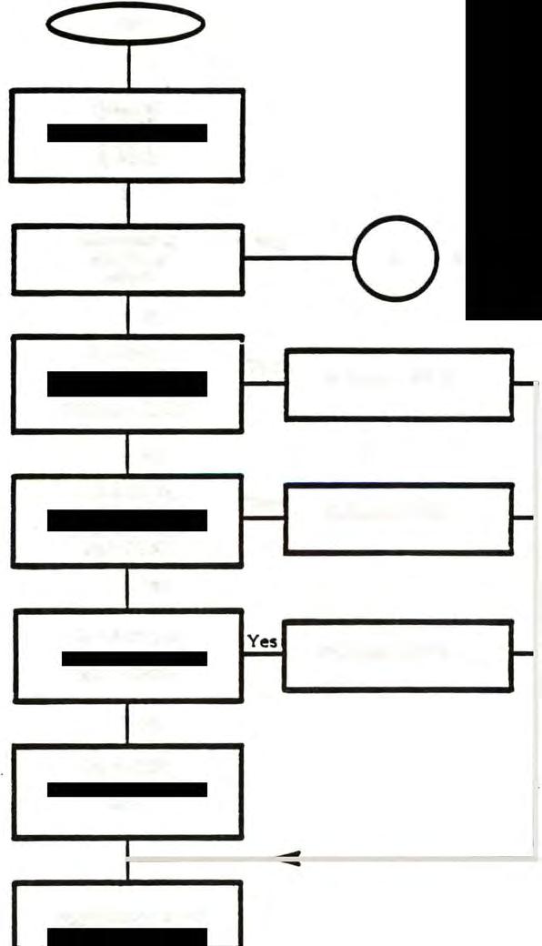
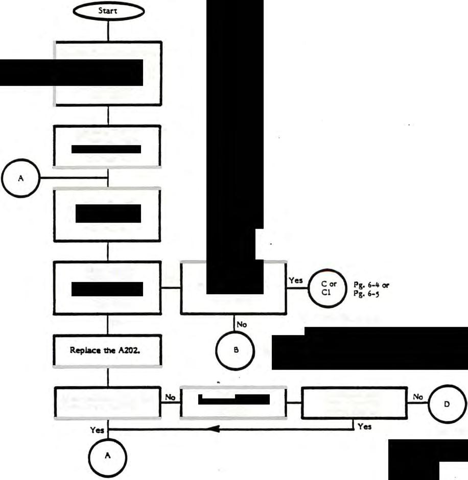
The Diagnostic Flowchart is intended to be easy to use and the primary aid when troubleshooting the 2600. Follow the prompts in the order presented. When a question is asked, follow the line from that box which best applies to the unit's condition. The figures referenced in the flowcharts are located at the end of this section. When a line terminates with a letter inside a circle, note that a page number (i.e., pg. 4--3) is near it. Turn to that oage, locate the letter in another circle, and continue the diagnosis. The flowchart leaves nothing to chance, it tells you when to perform a specific test, and when to replace components, and even when and how long to "burnin" the unit. "Burn-in" the unit for at least two hours after completing repairs.
When a problem is extremely difficult to diagnose, the flowchart sends you to the Signal Tracing Cartridge (STC) routine, "0" page 4--47. Due to the repetitive nature of the STC routine, no flowchart is used. Read and follow the instructions as directed. Should the STC procedure fail to isolate the problem, after carefully inspecting the switchboard and motherboard assemblies for shorted and/or open trace lines, and solder bridges swap all three chips (6507, 6532, and TIA). Should the problem still persist, call ATARI, Techline Specialist: Inside California at (800) 672-14-66 and Outside California at (800) 538-1535. Be certain to always burn-in the unit for two hours after completing repairs. This helps to ensure that intermittent problems are found and also greatly increases your customer's satisfaction with your repair work.
SWAPOUT PROCEDURES


Many places in the diagnostic flowchart, a box tells you to "swapout" a chip or a number of chips in a particular order. The "swapout" instruction means that you should replace the indicated components one at a time with a known good component of the same type. The VCS should then be tested with the new, known-good component in place to see whether the "swapout" solved the problem being checked. If the swapout did not fix the problem, the known-good component should be left in, and the next component inserted. Once the problem is solved, you then place the suspected bad chips one by one into the system to determine whether or not those you pulled out are truly defective. In this way, you avoid needlessly replacing good components.
CAUTION
Extreme care should be taken when handling the integrated circuit chips (A200, A20l, A202, A203). They are all y!:!y sensitive to static electricity and can easily be damaged by careless handling. Always keep the chips in their plastic carrier tubes or on conductive foam when not handling them. Make certain you are well grounded when handling the chips. Atari strongly recommends that you wear a conductive grounding band (which ties from your arm toground) when handling thechips.
The chips are also susceptible to damage from stress when being removed from or inserted into the sockets. Always use achip-pullerwhenremoving thechips. 00 not pry chipsout with a screwdriver or anyother tool.
Failure to follow the above guidelines results in unusually high chip failure rates and extra expense. •
SECTI ON 4
4-1 2600/2600A Domestic VC5
Vbua.I1yinspectswitches, jKIcsandconnec1arS. .�certainnoshorted or�tracesorsolder bridles...onthe board(s).
Connectvesto TVbatteryellminaUlr.SetTVto channell.
InsertOlqnostic Cutr"idle(OTC),initiallze(Fllure4-1) andturnon.
Does�ydefec:tiveRAM panem� onscreen(_ FiS·4-)·
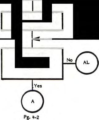
2600 Diagnostic Flowchart
ReplacetheA202.
No
Ispicture WVl*Iandrau..t onleftside ofSCNe'l?
Pg.�
Doesunitnowshowthe No <:alor barspanem?
Doesunitnow showthe color barspattern? ______ ____________________________ Ves
SwafIOUt I)A200 2)A202
4-2 2600/2600A Domestic yeS
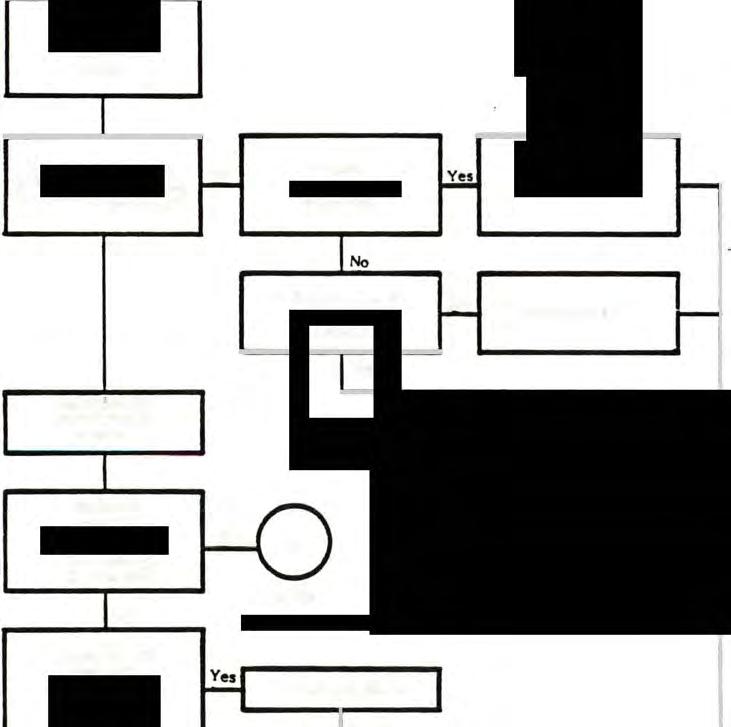
Are color bars present?
(See Figure 4-2). No
Is any other test pattern on the screen?
(See Figure 4-4, 4-6,4-9).
Are color bars properly adjusted?
(See Figure 4-2)
Check your switch settings. Are they correct?
Is there "snow" on the screen? (no modulation)
Check YCS connections to TV and channel setting. Test YCS with known -good battery eliminator.
Is ANY modUiation present on screen? No Yes Pg. 4-9 screen gone? �--------------------------------�--t
Is "snow"on Yes
2600 0iagnostic Flowchart (Continued)
No
Yes
Yes Yes No
No
Yes
4-3
Pg. 4-11
Pg. 4-6
2600/2600A Domestic ves
Pg. 4-2
Bad Video Troubleshooting

Use swapout procedureto identifybad· board.
Badswitchboard Pg.4-13 Badmotherboard _____ No DoesA203have goodVa:(.'vat pin&)andsround (atpin1)1 . Yes Checkthat thetraceUne from1\201 pin2 isnotshorted toanotherline. Isapicture nowprell!l'lton theTV? Yes Pg.�2 No Yes No Repairopentrace. Doesunitnowhave apic1ure? Check R234, C221,andR233. Replaceu nec:eauy. ReplaceA203. ReplaceR221 Swapout 1) 1\200 2)1\202 4-4 Yes Isapicture Ves nowpt'ell!l'lton theTV? Pg.1I-4 Isapicturenow prell!l'ltontheTV? Ves Pg. 4-4, 2600/2600A Domestic ves
Gray Bars Test Procedure
Place color/ black &: white switch in 8&:W .position.

Did screen pattern change when switch was moved ?
Yes
Is proper gray bar pattern pre nt? (See Figure 4-4).
Yes
Is a partial segment missing or is an color present (See Figure ,.-.5) Pg.4-14

4-5 No
2600/2600A Domestic VC
Pg. 4-7 Pg. 4-20 Pg. 4-4.5
Color Bars Test Procedure
Reconnect ves and initialize.
Are color bars present on screen?
Yes
Adjust R211 so that color is aligned properly. (See Figure 4-2).
Is ves tunable to proper shades?
4-6
Pg.4-23
Pg. 4-2
2600/2600A Domestic YCS
Pg. 4-'
On 2600 units, usesw.pout procedureto identifybad board.(See0Iart)
With inoperative switch in position (oper,), is+'vpresent at J201 pinforthat switch?(SeeClan)
Yes
Closethe switch.
Defective Switch Troubleshooting Procedure
Bad Switchboard
Istvnowpresent attheRAMpin forthatswitch? (Seechart)
Yes
S..,�
l) A202
2) A200
3) A201
DDetswitchnowworic?
Isthereanopen between J20I and RAM pin?
Yes
�it;'7 lor Black and White LeftDifficulty RightD1fflculty Select Reset Yes Pg. ,...311 Repairopentrace. CONNECTIONCHART J201 PinNo. 4-7 II , 7 ') a A202 � 11 17 16 Z3 2.
the
screen? Yes 2600/2600A Domestic VC
Doesswitch nowchange
pattern on
Defective
present? No
Switch Troubleshooting Procedure (Continued) Check RAM (A202) pin for the switch for .'v. Is it
No
No
No
1) A200 2) A201 Pg. �2 �-8
2600/2600A Domestic VCS
Check for shorted trace line. Repair as necessary. Does switch now work?
Swapout A202. Yes Does switch Yes now work?
Checkwhethercapacitor on that RAM lineisshortedto Yes ground. Replace as necessary. Does switch now work?
Swapout
Pg•.�-9
Black or Solid Colored Screen Troubleshooting
Use swapout Defective switchboard procedure to
Is
Is
Is
C J :::> 1
V
identify which board is bad. T
Pg. 4-16
Defective Motherboard
K
Pg. 4-10 Swapout
4-.5v
I) X200 osc.
� 2) Q200
between 3) Q201 C203 and R203? 4) Other Clock
Circuit Components
4-.5v H Yes .2 signal
presenton A202 pin 39? 1 No
Is
H
signal
present
rYes
4-5v p-p Open between osc.
No
I-- C203 and pin 11 � Reoair I-pin
A201.
signal
presenton
11 A201?
TYes
Swapout I-- Does
Il A201
2) A200
4-.5v p-p No
unitfunction? IYes .0signal
present on
pin 4 A201? I No 1 Yes
Openbetween
I-- Pin 27 AlOO pin 27 A200? and Pin 4 A201• .
4-.5v p-p � Swapout Yes 1) .40200 � Doesunit function? � 42 signal 2) .40202
pin
A200?
4-.5v H Open between 42signalpresent No on A201 pin 26? I-- Pin 26 .40201 and Pin 23 A200.
Open between Pin 39 A202 andpin 28 A200. A Pg. 4-2 �-9 2600/2600A Domestic ves
Pin 4 A201 shorted. I-- Is 4-.5v p-p Repair � signal No
present on
rYes Is
present on INo
23
1Yes Pin 23 A200 is shorted.Repair Is
I Yes
Black or Solid Colored Screen Troubleshooting (Continued)
Is�'vpoop �2 signal present on pin 26 A201?

Yes
Is there +'v and ground on all of A200, A201, A202, A2037 Yes
Reset and ready lines good? Yes Swapout
1) A200
2) A202
3) A201
Does unit operate properly?
'No Open trace between pin 26 A201 and pin 39 A202. No Open on line to +, or ground. No Open or shorted line.
 Pg.
Pg.
4-4' Yes ______ ________________________ Repair
4-10 2600/2600A Domestic V(
Pg. 4-2
Snowy Screen Troubleshooting Procedure, Motherboard
Use swapout procedure to identify which board is bad.
1-------1
Is +.5v present at J201 Pin 11
Bad switchboard.
Is +9v present at n01 Pin 21
Is +7.5-9.0v present at J20� (the power jack)? Check at bottom of board.
L
Bad motherboard. Pg. �-18
No
No
Yes Yes Yes No Yes Swapout 1) A202 2) A200 3) A201 Replace J201. Check for
trace line between J204 and
Pg. �-31 Pg. �12 Is modulation evident on the TV screen? Is modulation evident on the TV screen? Yes Yes
Is there continuity across no1pin27
open
J201.
Pg. �11 Pg. 4-1 1 No
Yes No
Voltage
4-11 Repair 2600/2600A Domestic ves
Is no� OK?
Replace J20�.
shorted to ground.
Snowy Screen Troubleshooting Procedure, 'v1otherboard, (Continued)
Is there continuity across J201 Pins 1,3,6, 10,11 ? Yes polarity of Is there continuity continuity checker. Do between +5V not put + line and ground?* probe on ground
*Caution: Observe
No No
Replace connector.
Is modulation evident on the screen?
Is there an open trace on either +5v or ground?
Yes Yes No ________________________________
Check for and repair any shorted traces or solder bridges. Is modulation evident on the TV screen?
Check for and replice shorted caps: C204,C201,C220, C239,C200,C214.
Is modulation evident on the screen?
____ ____
No
Pg. �2
Pg. �2
4-12 2600/2600A Domestic YCS
Pg. �11
Bad/No Color, Bad/No Sound Switchboard

Is RF mod output tuned to 61.2' MHz? (Channel 3) Yes--
Short across LIOI. Does color (or sound) reappear? Yes ReplaceLlOl.
I No No No �
Can unit be tuned to .l:2.. 61.2' MHz ( + .1' MHz)?
Yes
Is color (or sound) Yes now OK?
Replace RF modulator.
Replace RF � mOduJator.
Pg. 4-2
c
0 :::>
I
I
4-13
2600/2600A Domestic YCS
Gray Bars Troubleshooting Procedure
Is there a 3-'v Yes Ched< R222-R224 with p-p signalon the Ohm meter. Replace any A2a3 side of R222, failedor off-value R223,R224? resistors.
Pg. 4-4'
Do all of pins 2, Yes
There is an open line 12, and l' on Ala) between A203 and the have a signal present? resistors. Fix it.
Pg. �, Check inputs of Yes A203 (pins 3,11,14). Replace A203. Doeseach have a signal present?
Pg.4-2
Do all of pins ',7,8 Yes
Check for open on AlO1 have a signal lines between Ala1 present? and Al03. Fix.
Swapout Ala1 chip.
Pg. �l'
No
No
No
No
4-14 2600/2600A Domestic yeS
Gray Bars Troubleshooting Procedure (Continued)
C Q :::> 1
Picture Now IYes Go to matrix OK? (See test. � Figure 4-4) I No
Make sure R218, R219, R220 have +'v connected to top side. I
Check R218,R219, R220 for proper values. I Inspect traces around l.M lines for shorts or opens. I
Is picture now OK? Yes
(See Figure 4-4) 1 No
Swapout A200 'and then A202. I
Is picture now OK? Yes
(See Figure 4-4)
..-U:..0
0 Pg. 4-454-15 2600/2600A Domestic YCS
Pg. 4-20
Colored Screen Troubleshooting Procedure Switchboard
c v :::> Bad Switchboard
Is .'v at JI01 Pin I? Yes

Pg. 4-17
Tune RF mod. If RF mod cannot be tuned to 61.2' MHz at adjustment tuned to 61.2' MHz, (channel J, ••1' � hole. � replace it. MHz)Yes
Is RF mod. output No
Isvideo Check foropen trace signalpre- Yes or badconnection besent at JI0l � tween J201 and RF pin 121 module pin. Repair.
Is JI01 pin No 12 shorted to 10- Defective JI01. ground? Replace. Yes
Check for shorted trace. If noneis found, the RF module is shorted and must be replaced.
Pg. 4-2
No
.-()
� 4-16 2600/2600A Domestic YCS
Colored Screen Troubleshooting Procedure, Switchboard, (Continued)
cw ::> I
Is +9v present at llOl Pin 2? I No
Check that l101 pin 1 or 2 is not shorted to ground.
Is CIO1 shorted? Yes - Replace Cl01. I No
Replace voltage regulator (AIO!).

Check that CI0l, CI03, or Cl06 arenot shorted. Replace if shorted.
If +9V is still not present at llOl pin 2, then replace the regulator (AIO!).
I
I
I Pg. 4-20
4-17 2600/2600A Domestic VCS
Snowy Screen Troubleshooting Procedure, Switchboard
Is .'v present at llOl pin 1 on the switchboard? Yes
Is .'v at the RF modulator pin 3 C, pin mod) or pin 2 (3 pin mod)? Yes
Does RF modulator pin 1 havecontinuity to ground? Yes
Make sure RF module output istuned to 61.2' MHz. ( .!: .U MHz).
No
OpenbetweenAIOl
pin 3 and RF modulepin 3. Check for and repair opens beRF module pin 1 and llOl pins 6 and 10 (ground).
Repair
If there is still a white screen,check the ll02COMector. Replace as required.
If no modulation, the RF module is bad. Replace. Is there modulation?
 Pg. 4.-2
Pg. 4.-19
Pg. 4.-2
Pg. 4.-19
4-18
No 2600/2600A Domestic yeS
Snowy Screen Troubleshooting Procedure, Switchboard, (Continued) c Y � I
Check for and Is +'v at the Yes repair defective output of the voltage i--- J101 or open trace regulator (AI01, pin 3)? between J101 pins and AIOI.
I No
Is·unr�uJated
Check for Yes bad reguJator +7.'-9v at voltage - (AIOl) a. open reguJator input between ground (AI01, Pin 1)? and AI01.
I No
Is +7.'-9v present Yes RepJace S101. on the J101 side ofS101?
I No
Does JI0l pin No 2 have Icontinuity?
t Yes
Is J101 pin 2 1-- RepJace J101. $horted to �round? Yes
INO
Check that Cl03 or C106 have not shorted to ground. Ir Is there modulation?
es Pg. 4-18 Pg...., 4-19'-10t-2600/2600A Domestic YCS
Initialize switches, then push "left" difficulty switch down.
Does screen No match Figure 4-6?
Yes
Put in shorting plugs.
Does screen matchFiguret;-7'?
Yes
Push down "Game Select" switch (5106).
Did lower middle No block on screen tum black in center?
Yes
Push down "Reset" switch (510') Does lower middle block tum black on left and right ends? Pg.
'\11
atrix Test Procedure
4-24 4-20
Pg. 4-23
2600/2600A Domestic ves
Pg. 4-7
Color Troubleshooting Procedure, Motherboard
AA � I �
Use swapout Defective switchboard. procedure to 0 . determine which board is bad.
I Defective Motherboard
Pg. 4-13 X200 frequency � correct?
Defective X200. ... (3.'46 ! .04MHz)
I Yes
15 color very weak or not present at all?
I Yes
Pg. 1I-22
With R21 1 fully Swap counterclockwise Yes
1) A201 is there 6.5-7.'v � 2) A200 ton pin 10 A201?
I No
3) A202
Defective
Is there +6-7v on ,Yes C208,C209,R21 i the cathode of CR201? or open trace � between CR201 and pin 10 A20i.
I No
is there a 3-.5v p-p Yes
Defective CR200. signal on cathode �CR200?
I No
15 there a 3-'v p-p Yes
Defective signa! on cathode I-- CR201 � CR200?
INo
Open or shorted trace to diodes
Replace or Repair (CR200 or CR20l)
C
.--..,.....
4--21
11-2 2600/2600A Domestic VCS
Pg.
Color Troubleshooting Procedure, Motherboard, (Continued)
AS ::> Swapout
1) A20l
2) A202
3) A200
Does screen Yes now have
color?
Is J.'·'v
Pg. 4-2 p-p signal pre- Yes Defective R21..5. sent between Ie2lJ and R21..5?
Is J.'·'v p-p Yes signal present I- Defective C213 between C2l2 and C2lJ?

Is J.'-'v p-p IYes Defective C2l2 signal present pin 9 A20l?
Pin 9 A20l shorted to another line.
C
.-
A
�
No
No
No
No
-I Replace or Repair A � Pg. 1f.-2 4-·22 � � I2600/2600A Domestic VCS
Defective \I1atrix Troubleshooting Procedure
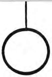
Isblueblade grid panef'n disrupted? (See Fisure es 11-.\ for examplebad panem)
Is upper left blocic on screendefective? (SeeFisure�or1J-1 for correct panern)
....re eimer the middle lower or the left lower Yes !:llocic defective? (See Figure�or1J-1 for correct panern)
Is upper-middle block detective?
Is lower-middle block defective? Pg.
Pg.
The panef'n may have errors. !:lut all nllle blocksare present on screen.
Is entire matrix now on screen?
Yes
PI!. 4-4,
Are mIddle-left �d lower-level blocks now correct (See Fi�ure Yes �or 1J-7)?
PIJ.....26
Yes
No
p!.IJ-i6 sw�t l)A200 2)A202 3)A201 swapout I)A202 2)A200 3)A201 swaoout I)A200 2)A202 J)A201
1J-20
1J-27 4-23
Is mIddIe.."iddle block now OK'? 2600/2600A Domestic yes
Audio Test Procedure
Reinitialize switches. Press down the "right difficulty" switch. Is there a dear tone? No
Use scope or frequency counter to measure frequency at emitter of Q202. Tuneaudio to .5.' MHz by adjusting L201. Adjust to !: .06 MHz. Look for stable frequency. Can unit be adjusted and is sound dear?
4-24
Pg. 4-28
2600/2600A Domestic VC
Pg.4-27
Are the two patterns in Figure 4-9 alternating on the screen?
Yes
Do the patterns alternate with the tones?
Yes
Are both colors and tones consistent each cycle?
Yes
Put switches back to initialized positions. ves will go through one last cycle before changing to color bar test.
Are patterns now correct?
Audio Test Procedure (Continued)
Pg.4-28 No Swapout 1) A201 2) A200 3) A202 No 4-25 Pg. 4-2/j.
Pg. 4-30
(As
/j.-9)
4-45 2600/2600A Domestic VCS Changed per ECN 110021 1/29/83
in Figure
Pg.
Defective I/O Lines Troubleshooting Procedure C
Check the RAM � Repair open trace Repair line to-- (A202) pin. Is.Sv between A202 pin
shorted to•Sv present there? andthe J203/J203. (Check tracelines>.
Check trace line(s) from defective pin(s)

Repair for shorts to ground. Are there any shorts? I No
Swapout A202.
Is .Sv now Yes present at the A202 pin?
Replace me capacitor on that line(seechart).
Does the Diagnostic No Swapout Matrix screen now l) A200 look correct(see Fig. 4-6) 2) A201
....F
T Defective A202 Cap. Connector Determine (RAM) Line No. No. Pin No. which lines olre IS CITs n02-Pin 4 defective by 14 C234 n02-Pin 3 refe!Tin� to LJ C233 n02-Pln 2 Figure 4-7. 12 C232 J202-Pin I I 11 C231 J203-Pin 410 n03-Pln 3 C230 9 029 n03-Pin 2 Check the lines & C22a 1203-Pln 1 indicatedas defective for •Sv at J202 or J203 (See chart). I Swapout Does Diagnostic
.Sv
l) A202 Matrix
the lln6(s)
2) A200
(See t--
J) A201 Fil!:ure 4-6
4-7)? lNo INo
�
Is
present Yes
now look Yes on
to--
to-- correct
just checked?
or
�
INo
P1
I
INo
I
I
/.j.-26 2600/2600A Domestic '
P�.4-2
Trigger Line Troubleshooting Procedure
C
Is •.5v atpin 6 Check/repair trace lines Check for VMOD Is trigger line of J203 (right) � from: R22' to J203, pin 6 (.'v) at top of Yes trigger)or 3202 (right), R226 to J202, - R22' (right> or now operating(left trigger)? pin 6 (left). R226 (left) corTectly?
Is•.5v at A203 Repair opentracefroml pin 7 (right � R22' to A203 Is triger line trigger) andpin9 (right> - now operatinl! (left trigser) R226 to A203 properly? (left> Yes Yes
Is�.>-'vat • Is trigser line ,It A203 Din 6 Yes (right) and SwapoutA203. I-- now operating Din 10 (left'? No corTectly?
Swapout A201
Doestriger Yes linenowwork properly?
Sw�
1) A200
2) A202
Doestrigser line Yes nowworkproperly?
Check/Repair C236,CR202 (left) C237,CR203 (right>
.....G :::>
Yes Na
Yes
No
No
I PI!. __2 4-27 2600/2600A Domestic yeS
Audio Troubleshooting Procedure, Motherboard
Useswapoutprocedure toisolatethe.,.bo.rd.
a.tmotherboard Ps. �--��--��--------�
Is therea2vpop square",avewttich alternatesbetween two frequencieson Pin 13 of A201?
Yes
Doessquare ",ave si�nalappe. at C210? Yes
Is therea••, MHz, modulated1-2vpop audio signa!atC211 (eitherside)? Replace 1)C211 2) R216
Isonefrequency appe.ing atthepin?
Yes Swapout A201.
FixopentraceIlne betweenC210 and pin 12/13or A201.
No
No
Is.'vatthetop of R201?
Yes
Pg. "-2"
Repairopen trace between J201 pin 1 andR201.
RepU-openbetween R201�A201 Pin 13.
Pg. "-29
Istherenowanalternatingaudiotone from theTV?
Pg.1J-2
4--28
2600/2600A Domestic ves
Audio Troubleshooting Procedure, Mot�erboard, (Continued)
Is there .'v at one end of L201? Yes
Check that L201 is good (has continuity and isn't shorted or cracked). Check/Replace
1) C206, C207

2) Q202
3) L202 if audio is still dead, check the trace lines around C2ll for opens and shortS:
No
Repair trace from VMOD (.'v) to L201.
Is there now an alternating audio tone from the TV?
Domestic
YCS
Pg. 4-28 4-29
Pg. 4-2 2600/2600A
Cartridge Test Procedure

AJ
OTC works, but YCS unit is still suspect. Plug in customer cartridge. if available.
Available
Connect, initialize. and turn YCS on with customer's game cartridge.
Does correct video pattern for that game appear?
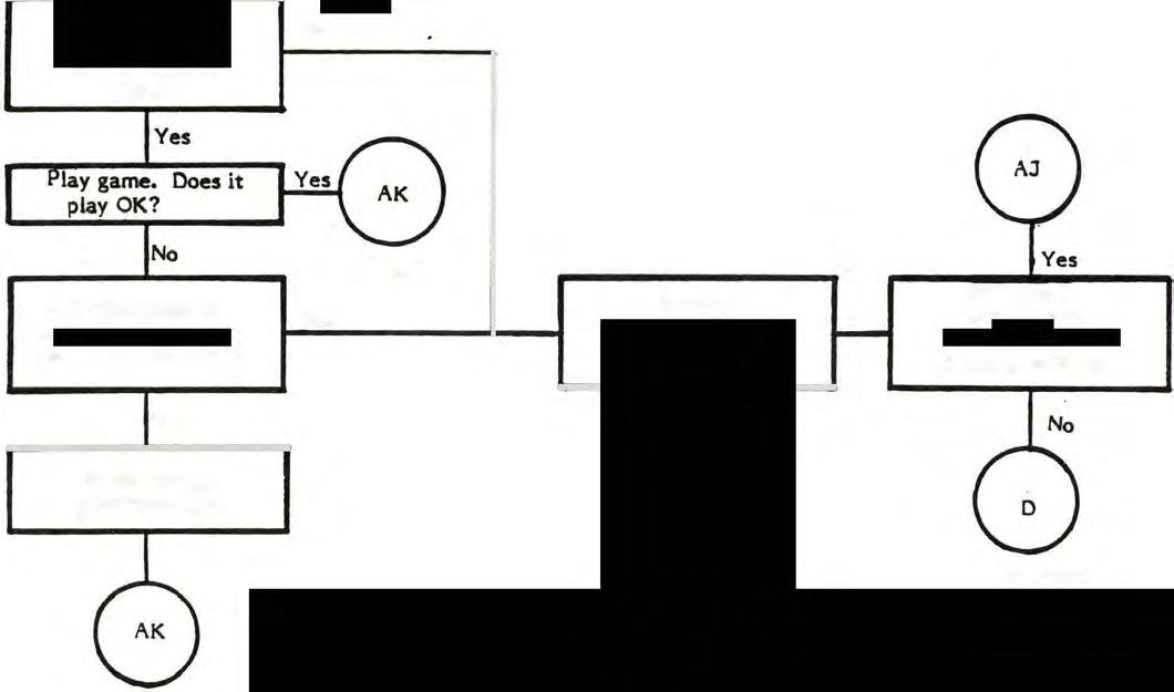
Check customer cartridge on known good game. Is it OK?
Replace with good cartridge.
Does game now operate properly with game cartridge?
No
No Yes
Pg.4-31
Not Available Pg. 4-31 Pg. 4-31 Swapout 1) A201 2) A200 3) A202 �-30
Pg. 4-45 2600/2600A Domestic YCS
Burn-In Procedure

Place customer cartridge in game, if available. Otherwise,use other game cartridge. Run game for 2 hours, minimum. Do not tum off during this period. Check game's operation.
Is game working properly?
Yes End of test sequence.
Pg. 4-2 4-31 2600/2600A Domestic yeS
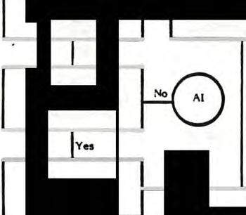
Defective Switch Troubleshooting Procedure
PutinoPerativeswitchin up(open) position.
Is+'vpresentatthe J201 pinforthatswitch (seeconnectionchart)? Yes
Istrace line shorted toground? No
Istherecontinuity aero. J201 connector?
Putswitenin down(closed) position.
Is.vnow presenton J201 pinfor thatswitch (seechart)? No
Isoneside01 switchtied,to groundushown inschematk? No
Repairopen between switchand ground.
Doespattern onscreen changewhen switchis flipped?
c AL
-
I No Yes P1
Yes A Pg.1J-2 Replaceswitch. 4-32 � Repair � INo Change jj;(jlCONNECTIONCHART Switch Color/SlackfI. White LeftDifficulty RightDifficulty Select Reset JIDI Pin No. 4 , 7 9 3 2600/2600A Domestic yeS
Snowy Screen Troubleshooting Procedure

i\M =>
Is there fV No on J201 pin 12?
Yes
ls there +5v
Is there Yes No an open line Repair. on pin 20 of I-- between pin � A201? 20 and +5v?

Yes I No
Swapout A201. Is there r modulation?
J No
Is there continuity No Replace no1 across J201 pin 12? I"Yes
Is J201 pin 12 Yes
Are C221 or Yes shorted to R223 shorted Replace - ground? (check -continuity) . to ground? No I No

Check for Swapout A201. solder bridges 10- Repairor trace shorts.
Is there � Swapout 1) A200 modulation? 2) A202 Yes . .. I
C
I
-
-
Pg. 4-2 4-33 2600/2600A Domestic ves
C Start
:::> T
Put shorting plugs in. Put ves into Diagnostic Matrix mode.
1r�
Paddle Lines Test
1 No
Repall' open Is ..aveform present on each of the A201 pins trace between - Dopaddle lines no.., Yes each of the pins shown shown in the chart? A201 and n02/ work OK? f.n03. in chart?
Check J202/J203 for RC waveform(see Fig. 4-10). � Doeswaveform appear at �
Yes No ,
S..,apout Il A201
2)A200
3)A202
Istherecontinuity between No Check tracelinesand the J202 or J203 � pin(seechartl resistors for opens. and the A20I?
Yes
Replace cap (C2l.5-c2lS) on the failed line.
DoetRC ..,ave1orm appear Yes on theappropriate J202 Of J203 line?(SeeOIart) INo
S..,apout I) A201
2)A200 ) A202 I
Does Paddle 1 Yes line now work? I INo
Paddle line isopen , Repair I or shorted. I
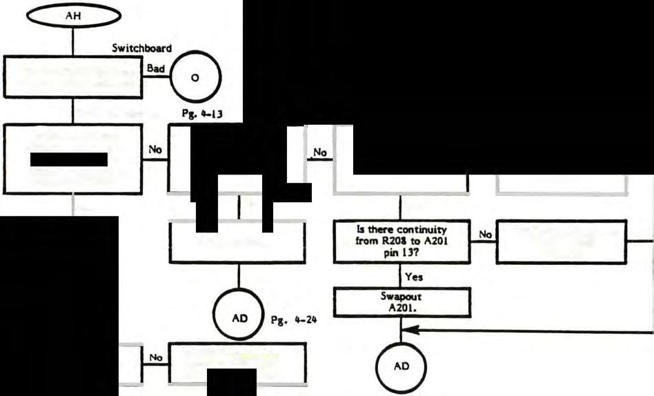
A ConnectionChart Pg. 4-2 Pin Pin Pin Cap Player A201 J202 m No. I 4l) -5 C215 2 39 9 C216 3 38 , C217 4 37 9 C2lS 4-34 2600/2600A Domestic yeS
NOTE: The following figures are referenced in the 2600/2600A Diagnostic Flowcharts, Sections 4 and 6, and are included here for your convenience. They can also be found in Section 3, where the tests are described in more detail.


Lt:FI CX2600
PONER TVTYPE CIFFICUcry
�/C:HT GAME G4ME OIFFICUI.If 'SELECT eESiET

initially to the left a CX2600A
�:
�:�:
�: �� ��
Figure 4-1. Switch Initialization Positions 4-35
2600/2600A Domestic yeS
NOTE: Set all switches to initialized position. A screen of horizontal color bars is displayed (see Figure 4-2). The screen should be steady and unchanging. A gray or blue horizontal reference line runs across the screen about three bars from its bottom. This reference line is thinner than the bars around it. R2ll (R2l3 on the 2600A board) should be adjusted so the bars immediately above and below the reference line are withinone shadeofeach other. Properoperationoftheunit isindicatedbybeingable to make this adjustment and by consistent color within the entire span of each bar on the screen. Minor glitches on the edges of the color bars are acceptable. Leave this test on for at least ten seconds in order to catch any intermittent problems, such as a bar momentarily changing colors or blanking out.
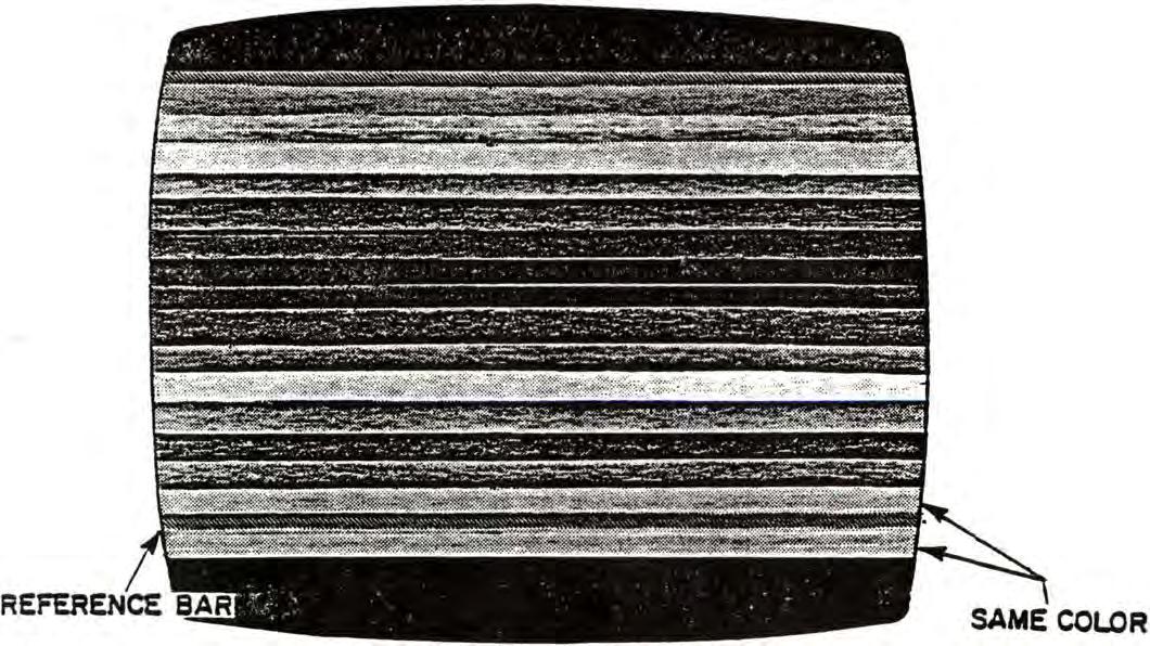
 Figure 4-2. Color Bars Screen
4-36 2600/2600A Domestic VC�
ANY DIAGONAL LINES ON THE SCREEN INDICATE A FAILURE IN THE RAM CHIP (AZ02).

/
Figure 4-3. Defective RAM Patterns
4-37
2600/2600A Domestic YCS
The gray bars screen has eight horizontal shaded bars. It is normal for the bars to have some uneven areas on their upper and lower edges. The bars must appear (in descending order> as going from black to white in even steps. The screen may not have any color in it. All eight bars must be consistent in their shade across the entire bar. The area of the screen outside the bars is irrelevant. The white line immediately above the top bar (black) is normal. This screen tests the operation of the chip set, especially the TIA (A202).
 Figure 4-4. Gray Bars Screen
4-38
2600/2600A Domestic yeS
This screen shows an example of a defective gray bars test screen. The appearance of a black rectangle in the middle of a light gray bar means that the data for that part of the screen has failed to be translated properly to the TV. Any disruption of the standard gray bars pattern (See Figure 4-4) or any color in the gray bars screen indicates a failure.
 Figure 4-5. Defective Gray Bars Screen
4-39 2600/2600A Domestic ves
The Diagnostic Matrix Screen appears as above, on a black background, when the shorting plugs are not inserted. The three left rectangles and the blue/black grid joinin them indicate the status of the I/o line connections to the 6532 RAM chip (A202


�! .s .s ... ... l � .. .. � ! .s .s ... ... 1 ID �! .s oS ... ... I Pink �!:: Il 2�3 .s oS .s .s .Ii ... ... ... ... ... 'H2 � � 'lI J � oS IDIDIDIDIDID Green 2 • :::: !::=� 0 .s .s .s .s .s .s ... ... ... ... ... ... 'H2 J 1 .! .. IDID c;,..., �!::=2� • 0 .s .s .s .s .s .s ... ... ... ... ... ... ";2 Pink • RICht j J � y'...... � :: II j j � � ! J l � Ii IDID J ID PHc...c;,..., Not\Joed J � � J � J ID J ID Gr..... Ga_ Ga_ Ga_ R_t Select R_t Swltd! Switch Swltd!
Green Not \Joed � J J IDIDID c;,..., Not \Joed J ! J IDOJID c;,..., Motu..!
Figure 4--6. Diagnostic Matrix Screen (Shorting Plugs OUT)
4--4-0 2600/2600A Domestic ves
I G(e� � ! :: � I� 2 .. .. 0 0 e .s .s .s .5 .5 c: a: Q. Q. Q. Q. Q. a: 612 .. 15 .. � .. 15 � � , .! .3 .3 .! Cii ., ., ., ., ., ., ... Green 2 .. � ! :: � = .. 0 0 .5 S e e .S .5 .5 .s Q. Q. a: a: .. Q. Q. .. �'J2 .. � .. .. .3 , , ... ... Cii Cii Green � ! :: � = 2 .. .. 0 0 e .S S .s .5 .s .s .5 a: Q. .. .. Q. .. a. a. �r Gr� II II Not Used :I R1sht ; Not Used ;E Trill'" ,!: w .:I .. .. ... ... ! .. !! .. � .. .3 , iii ... iii � Cii � � ... PinkorGr� NotUsed .. � � � .. .. !l , �� iii iii ... iii J G Green Game GAme GAme ReMt Select R""'t Switch Switch S..lt"h
4-41 Green Not Used .. � .. .3 .3 G ... ... Gr� Not Used � 1 J ... ... Gr� Not Used 2600/2600A Domestic yeS
Figure 4-7. Diagnostic \itatrix Screen (Shorting Plugs IN)
Any missing grid lines or disrupted rectangles indicate an I/O line failure (see page 4-26). Any missing or disrupted blue or black reference lines indicate that there has probably been a microprocessor failure (see page 4-23).
::: ! c: .5 ;;; Q. .3 ... ::: !. .5 S Q. ... � iii ::: ! .5 .S ... aI Pin" ::: � :: 2 .. .. 0 0 .S .S .5 .5 .5 .5 Q. Q. Q. a- Q. a'''1 J � J � .! .. .. .. .. Green 2 .. ::: � :: !: 0 .s .5 .s .s .s .s a... a- ... a- ... '''1 ! !I ! iii iii iii Green ::: � :: 2 .. .. 0 0 .s .s .s .s .s .s ... a- a- a- ... ... "t Pin" II Ii .. � RIs'lt .. .: TrlUef � :I .. .. .... .... J � .. ... J .. PI.. orGr..... Not Uted .. !I � J .. J � !iii ... � ... J .. Green e._ e._ e._ R....tSelectRetet S.ltcllSwltcllS.ltcII
Green NotUsed J 1 J .. ... ... Green Not Uted J J � ... ... Green HotUted
Figure 4-8. Diagnostic �atrix Screen with Defective Pattern
4-42 2600/2600A Domestic ves
Screens

The test displays two alternating patterns on the screen (as shown in Figure 4-9) while two alternating tones are heard. The tones change in sync with the screen. This test pattern continues for one full cycle after the Right Difficulty switch has been switched to stop the test.
@) -� e.� �/IA"( ........ "'''''''''3 d
Figure 4-9. Audio Tone Test
4-43 2600/2600A Domestic yeS


o .0o I r � � i·/ ! ,I , -'i i iI f I • s , I i I I I I I 1 I iI I I III II I I I I I IIr II I I , I ---- - -----c 2ms/div. lv/dive 00 Pin 37 and Pin 39 r """'I '0 I I I i I I 1 .0- j I I I Ii ' I I � IIIr...........,. I I 0 ,I- I 'YI i Ir I ,I- :/ I I ! I I I iV" I I i IIY' IIi I ! I I o Col I I I i I 1 I I <ill0 C 00 0 O � O J@.= OoO=0 --' �
2ms/div. lv/dive Pin 38 and Pin 40 2600/2600A
Figure 4-l0. RC Waveforms 4-44
Domestic VCS
SIGNAL TRACING CARTRIDGE (KLUGE) PROCEDURE

The Signal Tracing Cartridge (STC) is used to locate easily open or shorted traces in the address and data lines of the 2600/2600A. The STC causes the 6507 microprocessor (A200) to cycle through the entire memory space while executing "no operation" instructions. This is valuable because it puts a known signal on each address and data line. Then the signal can be traced through to the J200 connector, the TIA and RAM-I/O chips.
Since the STC procedure is not easily reduced to a flowchart, it is presented as a series of written instructions and illustrations on the following pages.
CAUTION: The STC procedure requires three known-good chips and a working clock circuit. The STC shouldonlybe used after allotherprocedures havebeen tried.
GETTING STARTED
Insert the STC into the 2600/2600A. Turn on the unit. The television screen should be gray or black. If it is "snowy" it indicates that you should return to the start of the Diagnostic Flowchart. Set the scope sweep to .5 microsec/division and set the vertical to 1 volt/division.
ADDRESS LINES AB0- AB12

Check the address lines at,the microprocessor (A200). Check address lines, starting with pin 5. A signal with a waveform similar to those shown in Figure 4-11 should be seen on the address lines, with each succeeding address line's waveform having a frequency half that of the line before it. For example, Al should be half the frequency of A0. If one or more of the address lines shows no signal, it is likely that the line is either open or shorted to ground or +5v. Check all traces and pins for shorts.


If you have a defective address line and it is not open or shorted, swapout the A200, A202 and A201, in that order.

If all address lines have signals, trace those signals to the J200 and the other chips. Table 4-1 illustrates which address lines connect to which pins on J200, 6532, and the TIA. The signal present on each address line of the microprocessor should also be present on each pin of J200, 6532, and the TIA connected to that line. If the same signal is not found, the trace line and/or solder joints between the microprocessor and the dead pin(s) is (are) broken. Check the trace lines carefully to locate the break.
DATA LINES DB0-7
Set the vertical on your scope to 2v/division. The data lines are tested very much like the address lines. The only difference is that the waveform seen on the data lines is different. The signals you should see are illustrated in Figure 4-12. If any data lines are completely inactive (simply remaining a constant voltage), it probably means that the line is either open or shorted to ground or +5v. Check the traces and pins for shorts. If none are found, one of the three chips or the STC itself orobably has an internal short. Try swapping out the 6532, TIA, and the microprocessor. Also carefully check noo for shorts between pins.

@
4-45 2600/2600A Domestic VCS
If all data lines have signals, trace those signals to noo and the other chips. Table 4-1 illustrates which lines connect to which pins of noo, 6532 and the TIA. The signal present on each data line of the microprocessor should also be present on each pin of J200, 6532 and the TIA connected to that line. If the same signal is not found, the trace line and/or solder joints between the microprocessor and the dead pin(s) is(are) broken. Check the trace lines carefully to locate the break.
Address lines (/), 7-12


Address Lines 1-6
Data Lines 0,2, and 4
Data Lines 1,3,5-7
I I I I ! I I I � L ! I I I I I 1 I I ! I I
1v/division I ; I I.. i i i I ! I : I I 1 I i I , I I I I 1 - I I : i� I I ; i I I ! I , I I i ! ! I 1 I I :II1 ..... i I fI I I J
1v/division
I I ; , i : I , � : , I i , I , 11IIm I II , I : 1I111ll11U
Figure 4-11. STC Address Line Waveforms
2v/division 2ms./division I i I I i I ii i i
2v/division 2ms./dlvision
4-46 2600/2600A Domestic yeS
Figure 4-12. STe Data Line Waveforms
-- Indicates no connection on that line
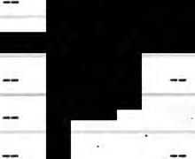
TABLE 4-1
ADDRESS A200 A201 A202 J200 LINES (MPU) (TIA) (RAM) Connector ABO 5 32 7 8 ABI 6 31 6 7 AB2 7 30 5 6 AB3 8 29 4 5 AB4 9 28 3 4 AB5 10 27 2 3 AB6 11 40 2 AB7 12 21 (CS3) 38 (CSt) AB8 13 22 AB9 14 36 (RS) 21 ABI0 15 19 ABll 16 20 AB12 17 24 (CSO) 37 (CSO) 18 DATA LINES: DBO 25 14 33 9 DBI 24 15 32 10 DB2 23 16 31 11 DB3 22 L7 30 13 DB4 21 18 29 14 DB5 20 19 28 15 DB6 19 33 27 16 DB7 18 34 26 17
Connected Pins on Motherboard
4-47 2600/2600A Domestic ves
SECTION 5
SYMPTOM CHECKLIST
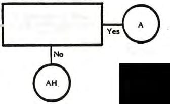
The Symptom Checklist is designed to assist the experienced technician arrive at a rapid diagnosis of VCS problems. The checklist is not intended to replace the Diagnostic Flowchart as the primary troubleshooting guide, but is designed to supple'ment the flowchart.
Symptoms have been divided into six general categories of failure:
• Logic
• Video
• Color
• Audio
• Controller
• Other
Each symptom is accompanied by some possible cuases and the best point to enter,the Diagnostic Flowchart to locate the problem.
5-1 2600/2600A Domestic VCS
SYMPTOM
Solid colored screen Vertical lines
2600 FAILURES
LOGIC FAILURES
POSSIBLE CAUSE (motherboard)
A200, A202, TIA
X200, Q200, Q20l, open or shorted Address or Data line
A200, A20I, A202, noo, open or shorted Address or Data line
DIAGNOSTIC POSSIBLE CAUSE FLOWCHART (switchboard) ENTRY POINT
AIOI, RF Module J, pg. 4-9 N/A J, pg. 4-9
VIDEO FAILURES
SYMPTOM
Snowy screen
Weak picture
Wrong Gray Bars
DIAGNOSTIC POSSIBLE CAUSE POSSIBLE CAUSE FLOWCHART (motherboard) (switchboard) ENTRY POINT
no power, A203
AlOI, LlOl, RF L, pg. 4-11 J20l, J204 Module, J101
LI0l, RF Module, X, pg. 4-1& RF Cable

A201, A203, N/A P, pg. 4-14 R21&-R220

N/A
5-2 2600/2600A Domestic VCS
SYMPTOM
No color
Only the reference bar appears
Color won't adjust
Weak color
2600 FAILURES (Continued)
COLOR FAILURES
POSSIBLE CAUSE (motherboard)
X200, A201
C208, R211
DIAGNOSTIC POSSIBLE CAUSE FLOWCHART (switchboard) ENTRY POINT
L101, RF Module AA, pg. It-21 RF Cable
SYMPTOM
010 audio
R21l, C208, C209
C212, C213, R215
N/A AA, pg. It-21 N/A - AA, pg. It-21
RF Module, L101 AA, pg. It-21 RF Cable
AUDIO FAILURES
DIAGNOSTIC POSSIBLE CAUSE POSSIBLE CAUSE FLOWCHART (motherboard) (switchboard) ENTRY POINT
Weak audio
DTC audio test fails
C206, C207, L201
RF module AH, pg. It-28 adjustment, Q202 adjustment
A201, C206, C207,
RF module AH, pg. It-28 L201 adjustment, adjustment C201
.'\201, A200, A202
N/A AD, pg. It-2lt
5-3 2600/2600A Domestic VCS
SYMPTOM
Fire button does not work
Joystick does not work
Driving Controllers
Paddle Controllers
2600 FAILURES (Continued)
CONTROLLER FAILURES
POSSIBLE CAUSE (motherboard)
A203, J202, J203, defective Controller
A202, J202, J203, defective Joystick
A202, J202, J203 defective Controller
A201, C215-C218, J202 - J203, defective controller
POSSIBLE ·CAUSE (switchboard)
DIAGNOSTIC FLOWCHART
SYMPTOM
Switches not working
OTHER FAILURES
POSSIBLE CAUSE (motherboard)
A202, C222-C227
DIAGNOSTIC POSSIBLE CAUSE FLOWCHART (switchboard) ENTRY POINT
5102-5106, JI01 AL, pg. 4-32
2600/2600A Domestic YCS
N/A N/A N/A N/A
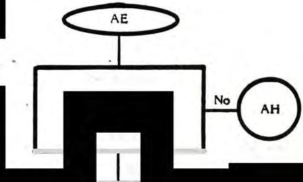
ENTRY POINT AG, pg. 4-27 AF, pg. 4-26 AF, pg. 4-26 pg. 4-34
5-4
SYMPTOM
Solid colored screen
Vertical lines
2600A FAILURES
LOGIC FAILURES (2600A)
DIAGNOSTIC
POSSIBLE CAUSE
A200, A202, A201, X200, Q200, RF Module
A200, A201, A202, J200, open or shorted Address or Data line
VIDEO FAILURES (2600A)
SYMPTOM
Snowy screen
Weak picture
. Wrong Gray Bars


Revisions 1-13
Wrong Gray Bars
Revision 14-
POSSIBLE CAUSE
A203, S201, RF Module, L205
RF Module, RF Cable
A201 , R218-221, R214--R217
A201 , R218-R221, R229, R230, CR202, CR203, R214--R217
Warped picture
Revisions 1-13
Warped picture
Revision 14-
A201, R221, R217
A201, R217, R221,R230, R203
5-5
FLOWCHART ENTRY POINT I, pg. 6-10 I, pg. 6-10 DIAGNOSTIC FLOWCHART ENTRY POINT K, pg. 6-12 K, pg. 6-12 M, pg. 6-14N, pg. 6-15 C, pg. 6-4Cl, pg. 6-5 .' 2600/2600A Domestic ves
SYMPTOM
No color
Only the reference bar appears
Color won't adjust
Weak color
2600A FAILURES (Continued)
COLOR FAILURES (2600A)
POSSIBLE CAUSES
X200, A20l, C2l0, C2l! RF Cable
R2l3, C205, A201P, pg. 6-16
R213, C205, CR200 CR201
RF Module, C210, C2l!, R210, RF Cable
AUDIO FAILURES (2600A)
DIAGNOSTIC FLOW CHART ENTRY POINT
P, pg. 6-16
P, pg. 6-16
P, pg. 6-16
SY�PTOM
�o audio
Weak audio
POSSIBLE CAUSES
C206, .C207, Q201, RF Module adjustment
A201, C208, R207, C206, C207, RF Module adjustment
DIAGNOSTIC FLOW CHART ENTRY POINT x, pg.
Diagnostic test cartridge audio test fails
A201, A200, A202
5-6
6-24
6-24
pg. 6-24 2600/2600A Domestic yeS
x, pg.
x,
2600A FAILURES (Continued)
CONTROLLER FAILURES (2600A)
SYMPTOM POSSIBLE CAUSES
Fire Button 1202, 1203 does not work Defective Controller
DIAGNOSTIC FLOW CHART ENTRY POINT
W, pg. 6-23
Joystick does
A202, ]202, 1203, not work Defective Joystick
Driving A202, ]202, ]203, Controllers Defective Controller
Paddle A201, C218-C221, Controllers J202, 1203, Defective Controller
OTHER FAILURES (2600A) .
SYMPTOM POSSIBLE CAUSES


Switches A202, C231-C235 not working 5202-5206
V, pg. 6-22
V, pg. 6-22 pg. 6-29
DIAGNOSTIC FLOW CHART ENTRY POINT
G, pg. 6-8
5-7
2600/2600A Domestic VCS-
SECTION 6
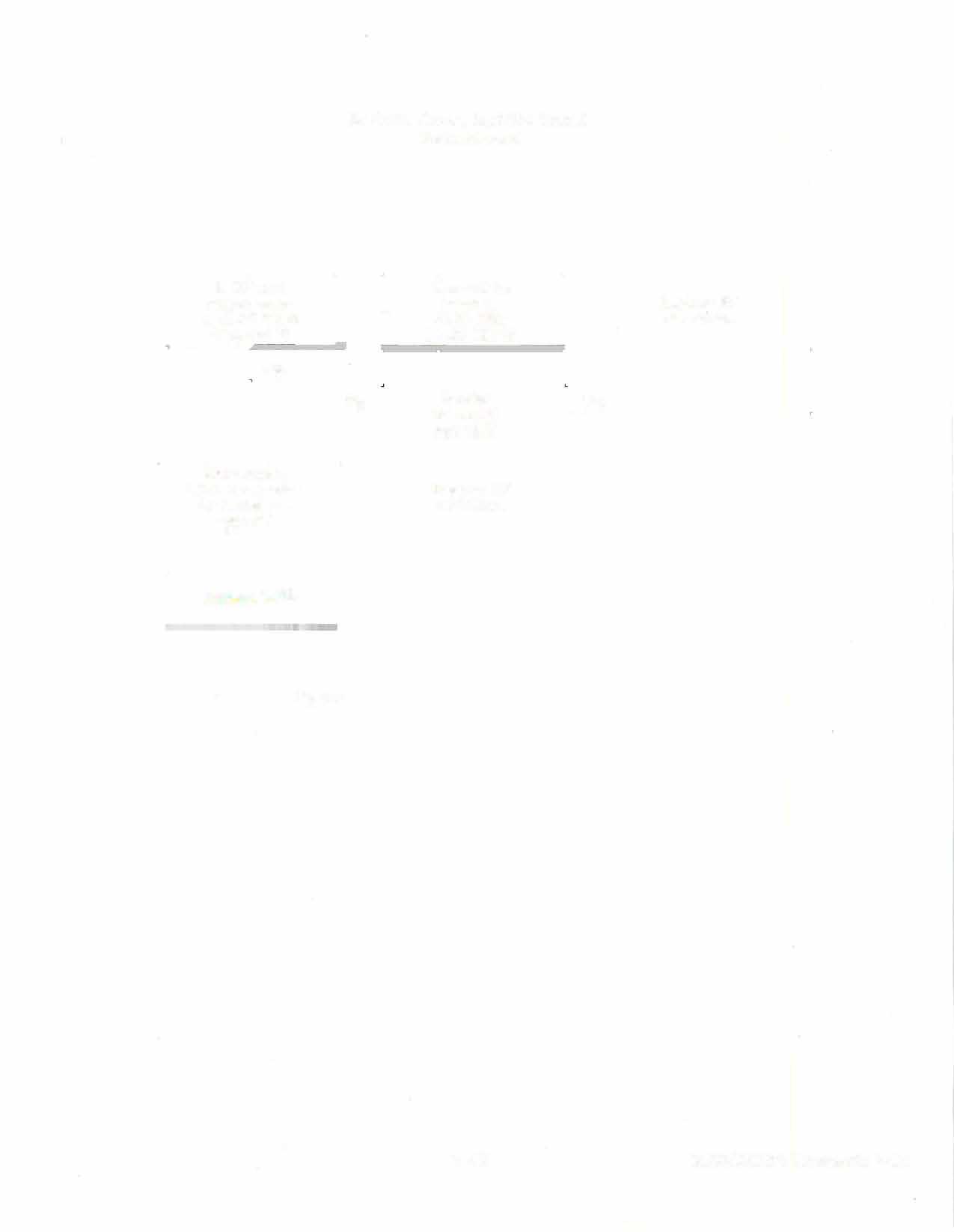
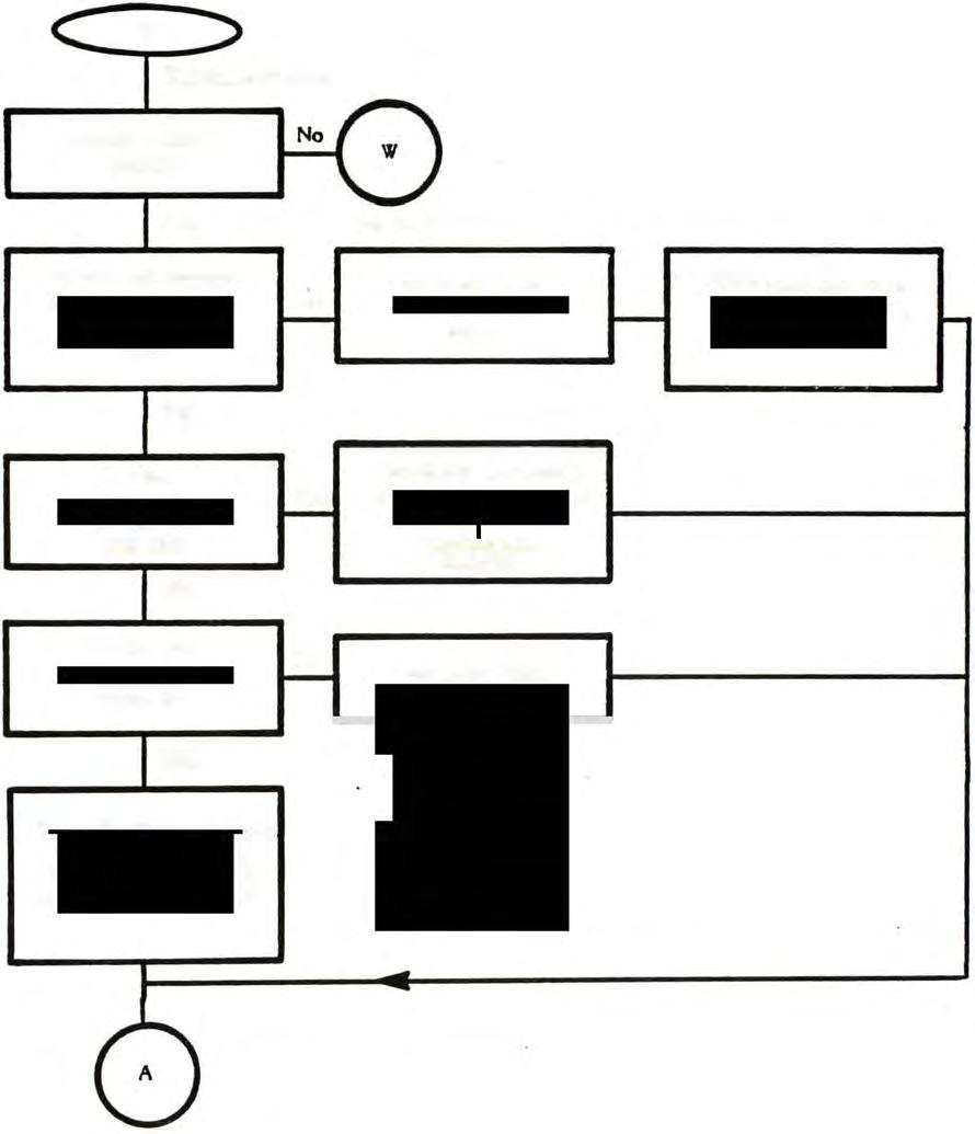
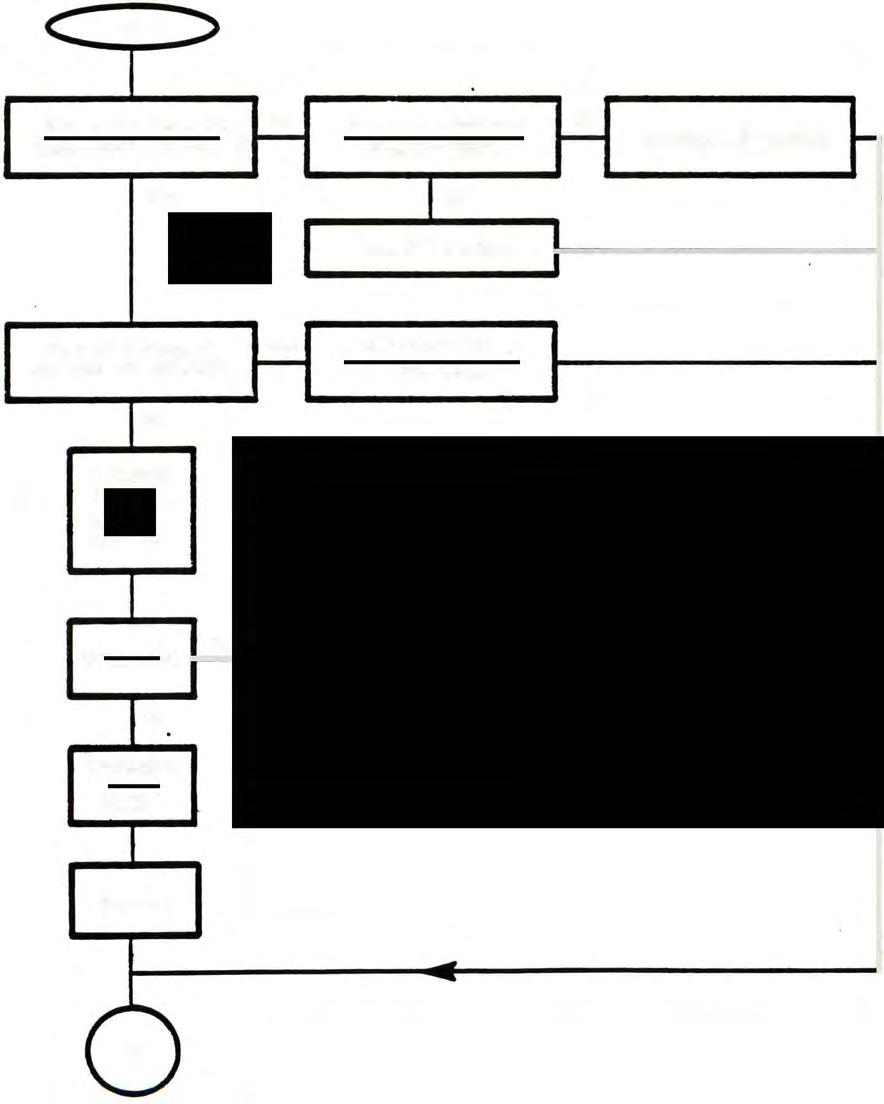
2600A DIAGNOSTIC FLOWCHART
The Diagnostic Flowchart is intended to be easy to use and the primary aid when troubleshooting the 2600A. Follow the prompts in the order presented. The figures referenced in the flowcharts are located at the end of Section 4, beginning on page 4-37. When a question is asked, follow the line from that box which best applies to the unit's situation. When a line terminates with a letter inside a circle, note that a page number (i.e., pg. 6-3) is near it. Turn to that page, locate the letter in another circle, and continue the diagnosis. The flowchart leaves nothing to chance, it tells you when to perform a specific test, and when to replace components, and even when and how long to "burn-in" the unit. "Burn-in" the unit for at least two hours after completing repairs.
When a problem is extremely difficult to diagnose, the flowchart sends you to the Signal Tracing Cartridge (STC) routine, "0", page 4-47. Due to the repetitive nature of the STC routine, no flowchart is used. Read and follow the instructions as directed. Should the STC procedure fail to isolate the problem, after carefully inspecting the motherboard assembly for shorted and/or open trace lines and solder bridges, swap all three chips (6507, 6532, and TIA). Should the problem still persist, call ATARI, Techline Specialist: Inside California at (800) 672-1466 and Outside California at (800) 538-1535. Be certain to always burn-in the unit for two hours after completing repairs. This helps to ensure that intermittent problems are found and also greatly increases your customer's satisfaction with your repair work.
SW APOUTPROCEDURES
�any places in the diagnostic flowchart; a box tells you to "swapout" a chip or a number of chips in a particular order. The "swapout" instruction means that you should replace the indicated components one at a time with a known good component of the same type. The YCS should then be tested with the new, known-good component in place to see whether the "swapout" solved the problem being checked. If the swapout did not fix the problem, the known-good component should be left in, and the"next component inserted. Once the problem is solved, you then place the suspected bad chips one by one into the system to determine whether or not those you pulled out are truly defective. In this way, you avoid needlessly replacing good components.
CAUTION:

Extreme care should be taken when handling the intergrated circuit chips (A200, A20I, A202, A203). They are aU � sensitive to static electricity and can easily be damaged by careless handling. Always keep the chips in their plastic carrier tubes or on conductive foam when not handling them. Make certain you are well grounded when handling the chips. Atari strongly recommends that you wear a conductive grounding band (which ties from your arm to ground) when handling the chips.
The chips are also susceptible to damage from stress when being removed from or inserted into the sockets. Always use a chip-puller when removing the chips. Do not pry chips out with a screwdriver or any other tool.
Failure to follow the above guidelines results in unusuaUy high chip failure rates and extra expense.

6-1 2600/2600A Domestic ves
Visually inspCt,witches, jacksandc:cnnectors. Makec:ertainno shorted oroptII'I tracesor solder bridSesareon the bovd(s).
Connect YCS to TV battery eliminator.Set TV to channel3.
2600A Diagnostic Flowchart
. INert OiaSnostic Cartridse(OTC). initialize (Fisure -.1) andtumon. .
DoesanydefectiveRAM pattern &ppeU' onscreen(see FiS· 4-3).
Ves
Doesunitnowshowthe colorbanpattern?
No lspicture warpedand raged onleftside ofJCreen?
C - 2600A Revs. 1-13
Cl- 2600A Revs. 14 andup
Pg. 6-3
Swapout
1)A200
2)...202
Doesunitnow !how thecolor bars pattern?
Pg. 4-4,
r---------------�------------------�yes
6-2 2600/2600A Domestic yeS
. Are color bars present?
(See Figure 4-2). No
Is any other test pattern on the screen?
(See Figure 4-4, 4-6,4-9). No
Is there "snow" on the screen? (no modulation)
Pg. 6-7
Are color bars properly adjusted?
(See Figure 4-2)
Ched< your No switch settings. Are they correct?
Is '''snow'' on Yes
screen gone? �------------------------------------1
Pg 6-12
2600A Diagnostic Flowchart (Continuec)
B
Yes
Yes
No
Check VCS connections to TV and channel setting. Test VCS with known - good battery eliminator.
Yes
Yes
6-8 No
Yes
Is ANY Pg.
modulation present on screen?
Pg. 6-10
6-2 6-3 2600/2600A Domestic ves
Pg. 6-6 Pg.
2600A Bad Video Troubleshooting (Loss of Sync.) (Revisions 1-l3)
R F module tuned to Can R F module be 61.25 MHz? (Channel 3) -- properly tuned? - Replace R F module '-
Tune R F module
3.5-5V P-P signal Yes Defective R217 or on A201 side of R217. � bad 1\20l.
1) A201
2) A200
3) A202
Domestic
c
C
:::> No
No
Yes I Yes
I
I
No
Swapout
Good
Yes No Defective R221 Replace_..... 1\Pg. 6-2 6-4 2600/2600A
ves
video
2600A Bad Video Troubleshooting (Loss of Sync.) (Revisions 14 and up)
R F module tuned to � Can R F module be No 61.25 MHz) Channel 3 ? properly tuned? I-- Replace R F module. � Yes
yes
Tune R F module. I
Defective R217 or on A201 side of R217. I--- defective CR203. or defective A201. No
3.5-5V P-P signal Yes
Swapout
1) A201
2) A20a
3) A202
Good video : Yes -
Defective R221 or R23C Replace.
Pg. 6-2
C
Cl
::>
I
I
I
I
No
6 -
I -
6-5
2600/2600A Domestic ves
2600A Gray Bars Test Procedure
Place color/ black de white switch in BdeW position. Did screen pattern change when switch was moved?
Is proper gray bar pattern present? (See Figure 4-4).
Is a partial segment missing or isany?color present . (See Figure 4-')
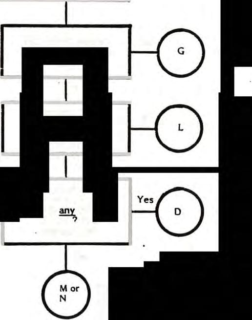
Yes
Yes
No No No Pg. 6-14 or 6-15 M .. 2600A Revs. 1-13 Pg. 6-8 Pg. 6-13 Pg. 4-45 N - 2600A Revs. 14 and up 6-6 2600/2600A Domestic yeS
2600A Color Bars Test Procedure
Reconnect ves and initialize. Are color bars present on screen?

Yes
Adjust R213so thatcolor is aligned properly (See figure 4-2). Is ves tunable to proper shades?
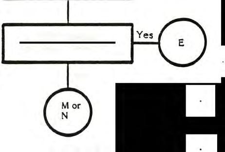
No
Pg. 6-14 or 6-15
M - 2600A Revs. 1-13
N - 2600A Revs. 14 and up
6-7 Pg. 6-2
2600/2600A Domestic YCS
Pg. 6-6
2600A Defective Switch Troubleshooting
With inoperative switch in open position, is there .'v present at the A202 side of it? Yes
Close the switch.
Is 0v now present at the RAM pin for that switch? (See chart)
Swapout
I) A202
2) A200
3) A201
Is there an open between No A201 and that switch?
I s switch connected to ground on other side?
Does switch now work? Yes Yes Replace switch.
Repair trace.
Pg. 6-2
2600/2600A Domestic yeS
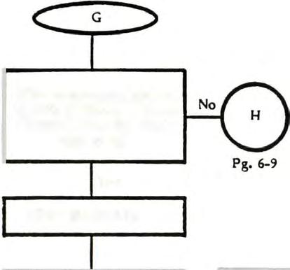
No
Yes
No ��----------------�
6-8
CHART Switch Color/Black and White Left Difficulty Right Difficulty Select Reset A202 Pin No. 21 17 16 23 24
CONNECTION
2600A Defective Switch Troubleshooting (Continued)
Is switch internally shorted?
Is cap on that line shorted to ground? (See chart)
Is there +5v on the RAM pin for that switch? (See chart)
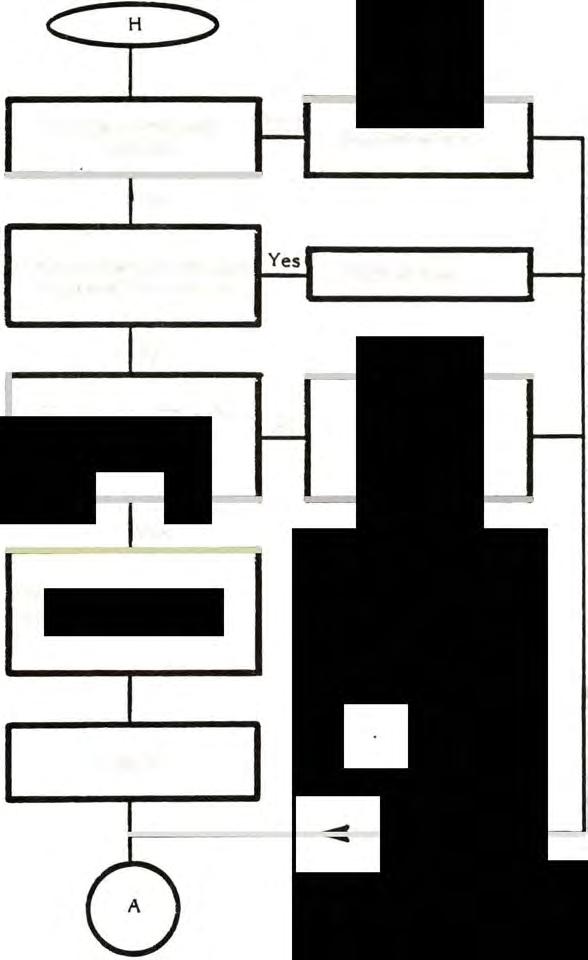
Open between RAM pin and inoperative swi.tch.

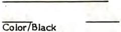
No
No
Yes
Repair Pg. 6-2 Yes No Replace switch. Replace cap. Swapout 1) A202 2) A200 3) A20I 6-9 CONNECTION CHART Switch Color/Slack and White Left Difficulty Right Difficulty Select Reset A202 Pin No. 21 17 16 23 24 2600/2600A Domestic VC
Is 4_'v p" 02 si�nal present on pin 23 ....200"? Yes
2600A Solid Colored Screen Troubleshooting
Chan�e
I) X200
2) Q200
3)Other clock cirClJit comoonents
Open between R204 and pin II :".201.
S,.,apout
I) ,0.200

2) ,0.202
P�. 6-2
Open between pili 27 ....200 _____________ and pin 4 ,0.201.
SwaOOlJt
1) A201
2) A20n
No Open betweenpin 26 ,0.20I and pin 23 ,0.200.
Does unit function?
Pin 4 A20I shorted. Repair
Yes
Pg. 6-2
Yes
6-10
2600/2600A Domestic VCS
2600A Solid Colored Screen Troubleshooting (Continued)
Is 4-5v p-p 02 signal present on A201 pin 26? Yes
Is there +5v and ground on all of A200, A201, A202, A203? Yes Reset ready lines good? Yes
Swapout
1) A200
2) A202
3) A20I Does unit operate properly?
No Open trace between pin 26 A201 and pin 39 A202. No Open on line to +5v or ground, or bad regulator. No Open or shorted line.
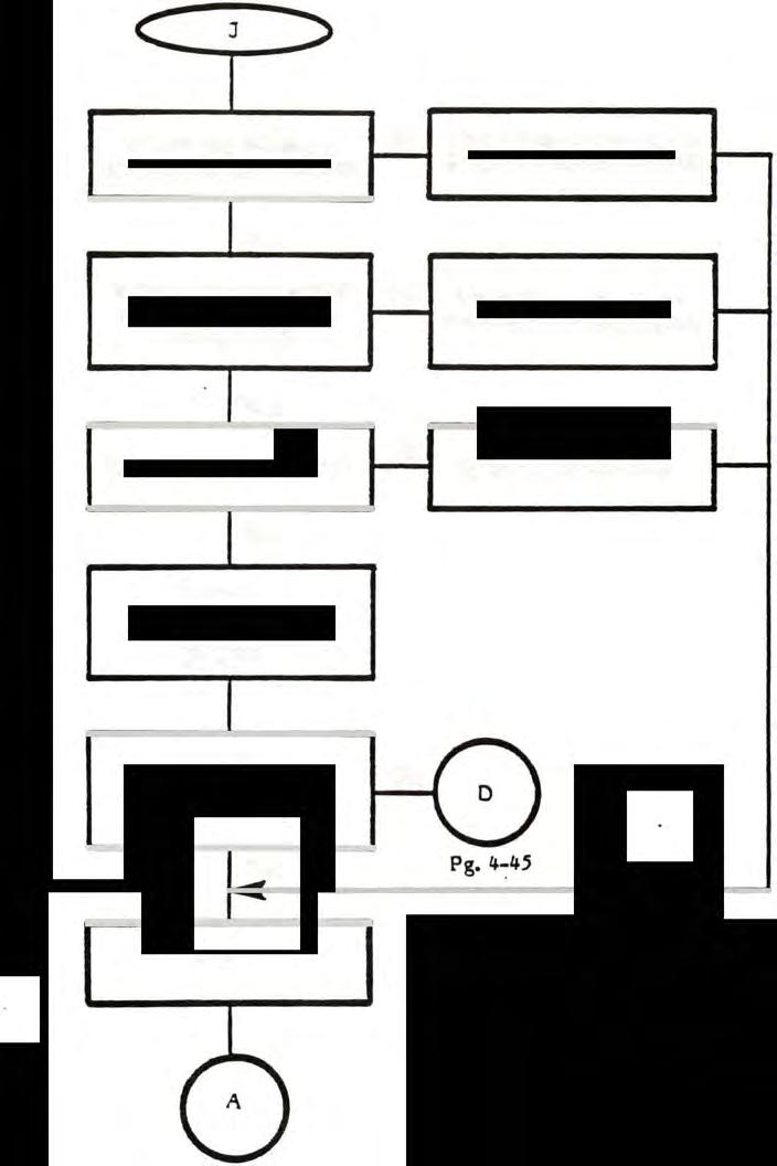
Yes Repair
Pg. 6-2 No 6-11 2600/2600A Domestic yeS
2600A Snowy Screen Troubleshooting Procedure
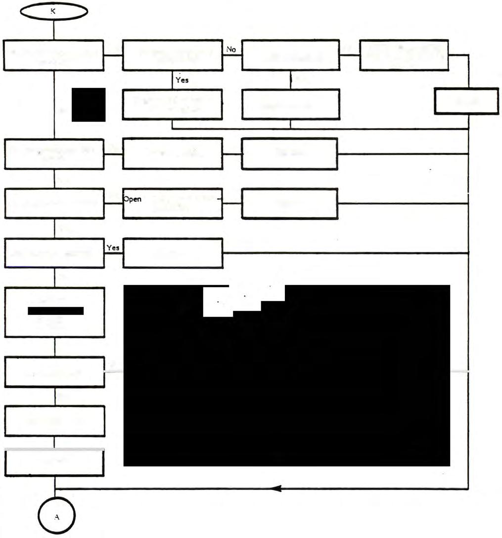
C '< :::> Yes � �o Open between A203 I-- Is·5v present on output � Is there +5v onfin 4 L205 defective? fo- output and RF module of �203? RF module. pin II. Ives t Yes Replace RF module or Replace L20'. I Repair I No bad RF cable? I 7.5 unregulated on :\203 Yes Defective A203. Replace input? I-- � No Yes pen between J201 and in 7.5 unregulated on 3101? put A203. I-- Repair :--10 +5v shorted to ground? IYes Repair No Swaoout L).�201 2)A200 J)A202 Yes Anv modulation? No Defective nOL. Replace I ?g.6-2 6-12 2600/2600A Domestic ves
2600A \'\atrix Test Procedure

initjalize switches, then push "left" dillic:u!ty switch down.
Does SCT'een No match Figure �6?
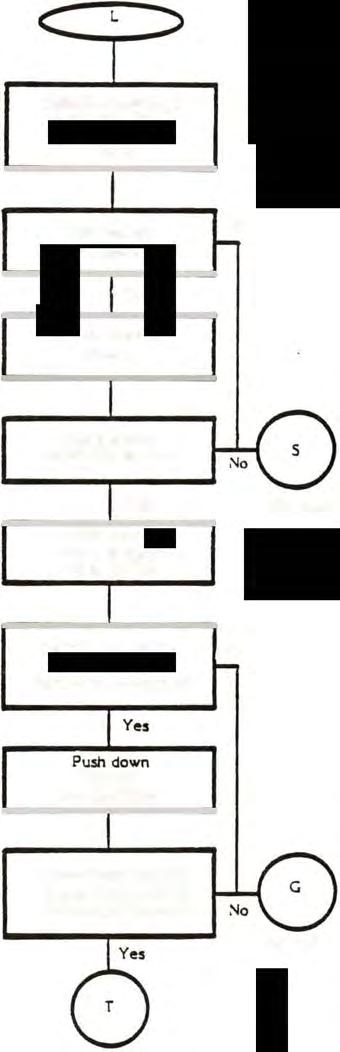
Yes
Put in shorting plu�s.
Does screen match F:gure �7?
Yes
Push down "Game Select" switch (5 106).
Did lower middle No block on screen tum black in center?
"Reset" switch (5 10')
Does lower middle block turn black on left and ri�ht ends?
6-13
Pg.6-17
Pg. 6-16
2600/2600A Domestic VCS
Pg. 6-8
2600A Gray Bar Troubleshooting Procedure (Revisions 1-13)
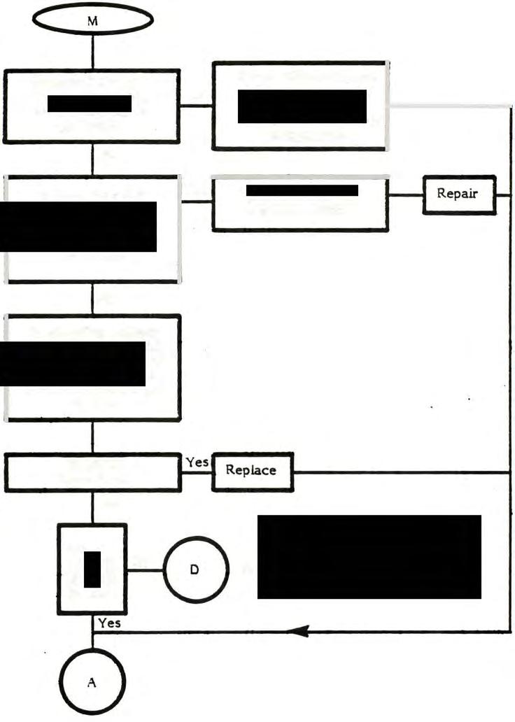

Is there 3-5v p-p signalon the A201 side of R214, R21.5, and R216? No
Is there 3-5v P-P signalon the A201 pin corresponding to the resistor that had no signal? No
Check pullup resistor R218, R219, or R220 on that line to insure resistor is good and one side is connected to +5v.
Resistor Defective? No Swap
1) A201 No
2) A200
3) A202
Check R214, R15, and R216 with meter for correct value. Replace any defective components.
Open between A20I and that resistor.
6-2 Yes Yes
Pg.
Pg. 4-45 6-1� 2600/2600A Domestic yeS
2600A Gray Bars Troubleshooting Procedures (Revisions 14 and up)

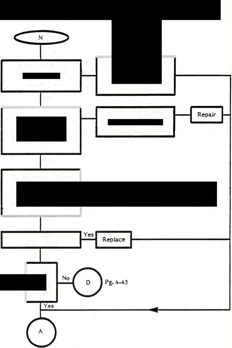
Is there 3-5v p-p signal on the A201 side of R214, R215, and R216? No
Is there 3-5v P-P signal on the A201 pin corresponding to the resistor that had no signal? No
Check pullup resistors R218, R219, or R229 on that line to insure resistor is good and one side is connected to +5V.
Resistor Defective? No Swap
1) A201
2) A200
3) A202
Pg. 6-2
Check R214, RU, and Yes R216 with meter for Yes
correct value. Replace any defective components.
Open between A201 and that resistor or defective CR202 if LM1 is bad.
6-15 2600/2600A Domestic y.
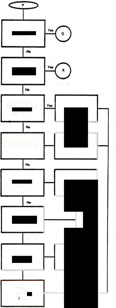
2600A Color Troubleshooting c p � I Ia.",color.,1aiIMe �re__ _I? I'" 'Io'-17 Is"-•z.z."",..,IiInU on.z.h.....__ IUlO..Cll? 1'" ,..'-II IsIMrWa2J.,.,,.., ..!::.. siena'....J-lll¥OIl Ile!tIaQCll � t.weI__ClO ..Cll? I'" b"-••,.,.",,..,� Yet __ClO..R22J? - Ile!t'-CIO I-1,.. Ia"-•.,.,.", y- ep..__T1APIn, ,..,aIpIUonpill, I-- ..ClG. ofTIA. 1,.. No IaR22Jpod? 1YNo RepairorIle!tlace IaRlIIpoet? t-l Yet SwapIUt 1)A201 2)A202 ) A200 A 6-16 2600/2600A Domestic VCS
2600A Color Troubleshooting (Continued)
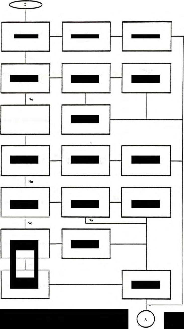
Co � 1
lscolOrconstantly :-10 Deiecuve roUin�(cycliny'? t-- I) C20' I-- Re?iace �
2) A201
Yes SwaDout
Does voltal\e vary between Yes Is Y200 !reauency Yes I) A201 ; .!c 6v on om 10 ot .�201 t-- ).'7'1' .\\Hz? � Z) A200 "hen R21J isrotatec'? ) A202
Tum R21J tully clockwise. �eoiace Y200.
!s tnet'ebVon anode 01 Yes I-- I)eiecnve R21J orooen I-- Repu or Rep�e CR200'? oetween R7 and A201. �
Yes Yes
,.jv on anode of CR201?I-- Is R212 �ood? I-- Detective CR200.
.) �n catnode ot CR20I. I-- Detective CR201.
Open between .,Jc CR20I Repair or Replace .
I
I� 1:-10
I
I�
I�
l.� Yes
I
�o
6 6-17 ?�.6·2 2600/2600A Domestic VC�
2600A Color Troubleshooting (Continued)
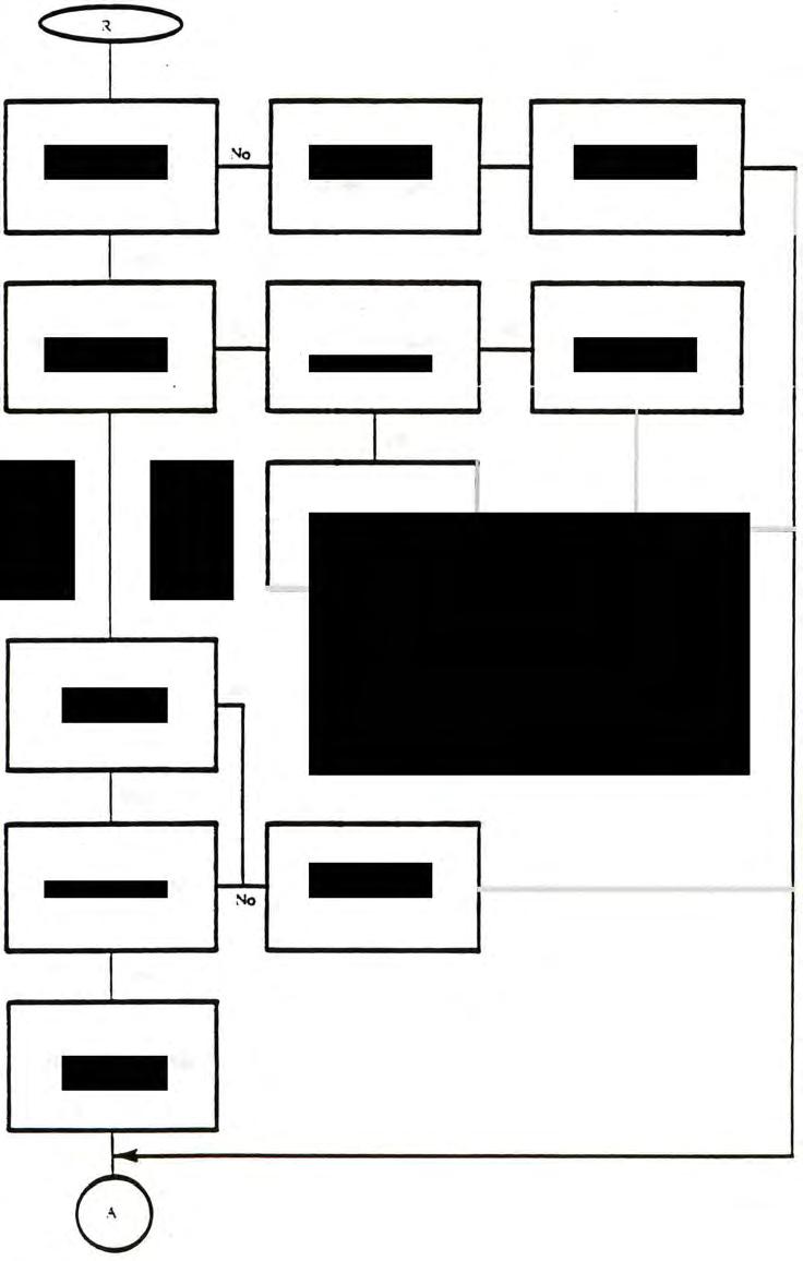
c � :::> Y2:JO frequency � Detective R�lace ).579':.;O�? 1) Y200 l- I-2) Q200 & Q20 Yes �o Can RF \1odule be � Is RF frequency l- I-- R�lace RF module. 01.2'\1Hz::.1'? tuned PfOIMrly? IYes Yes Tune RF module• . � R2U �ood? toYes Is RF callie good? �� R�laee Yes ReDlaee RF \1oduJe I P�.�-2 6-18 2600/2600A Domestic VC
are missingor some portion of the Matrix fails to appear on the TV screen.
2600A Defective \i\atr ix Troubleshooting Procedure

Is blue black rid pattern dis upted? (See Figure �8 for example bad pattern) No
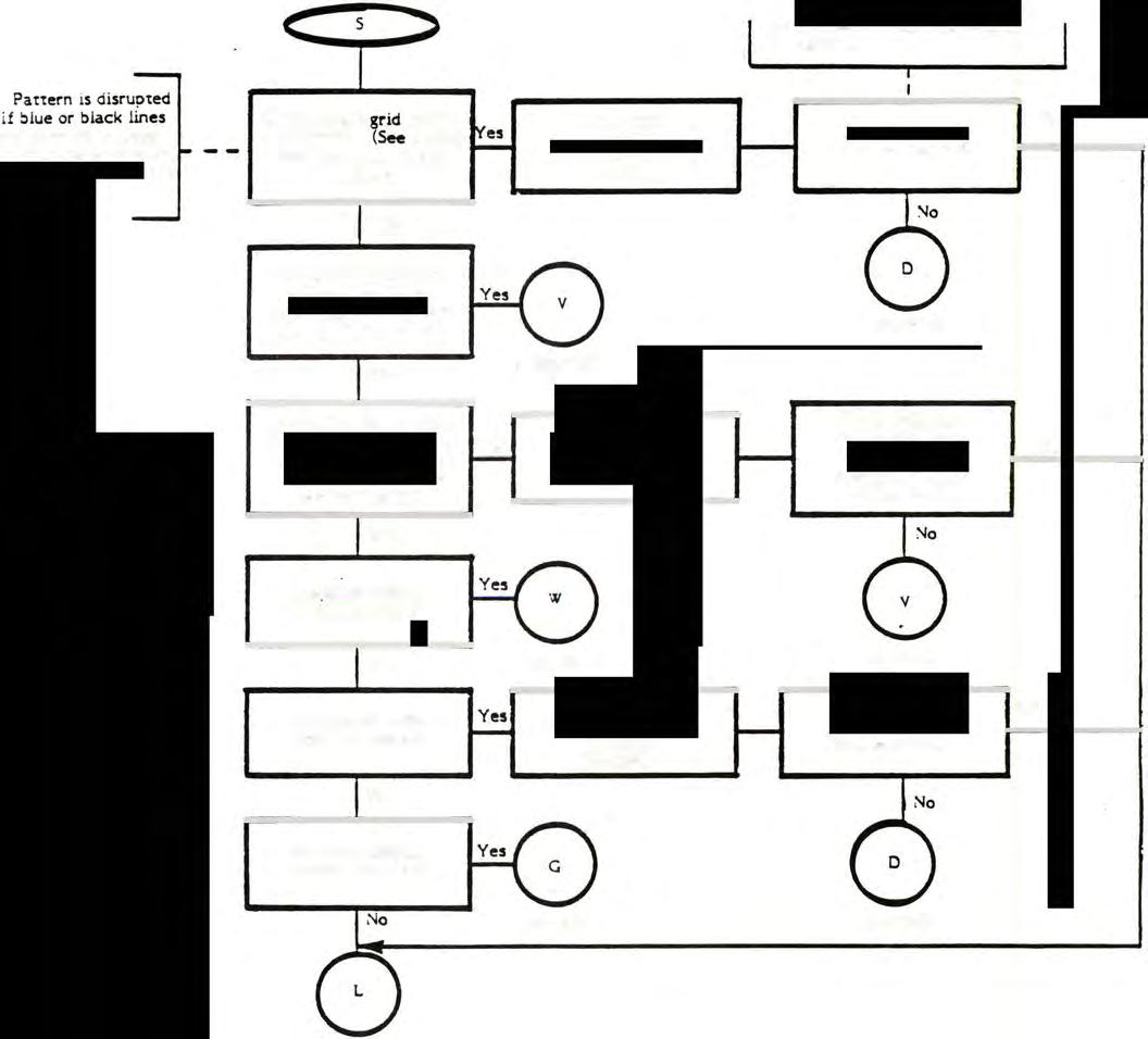
Is uppe left block on screen defective?
(See Figure �-6or�-7 for correct pattern)
Pg. &-22
Are either the middle lower or the left lower Yes block defective? (S-Figure �-6or4-7 for correct pattern)
tsuDper-middle block defective?
ts middle-middle block defective?
Pg. &-23
Swapout 1) A200
2) A202
3) A20 !
The pattern may have �r!'ors. but all nine blocks are present on screen.
Is entire matrix now on screen?
Yes
Pg. �4�
Swapout 1) A202

2) A200
3) A201
Are middle-left and lower-level blocks now correct (See Figure Yes 4-6or4-7)?
Swapout 1) A200
2) A202
3) A20 1
Is Iower-middle block defective?
Pg. &-8
Pg. &-1 3
Pg. &-22
Is middle-middle block now OK?
Yes
No
No
No
No
6-19
Pg. �' 2600/2600A Domestic yes
2600A Audio Test Procedure
T Reinitialize switches. Slide the right difficulty switch to the right. Is there a clear tone? No
Use scope or frequency counter to measure frequency at emitter of Q201.
Tone audio to 4.5 MHz by adjusting L201.
Adjust to ! .06 MHz. Look for stable frequency. Can unit be adjusted and is sound clear?
6-20
Pg.6-24
2600/2600A Domestic ves
Pg.
6-21
Are the two pattern� in Figure 4-9 alternating on the screen? Yes

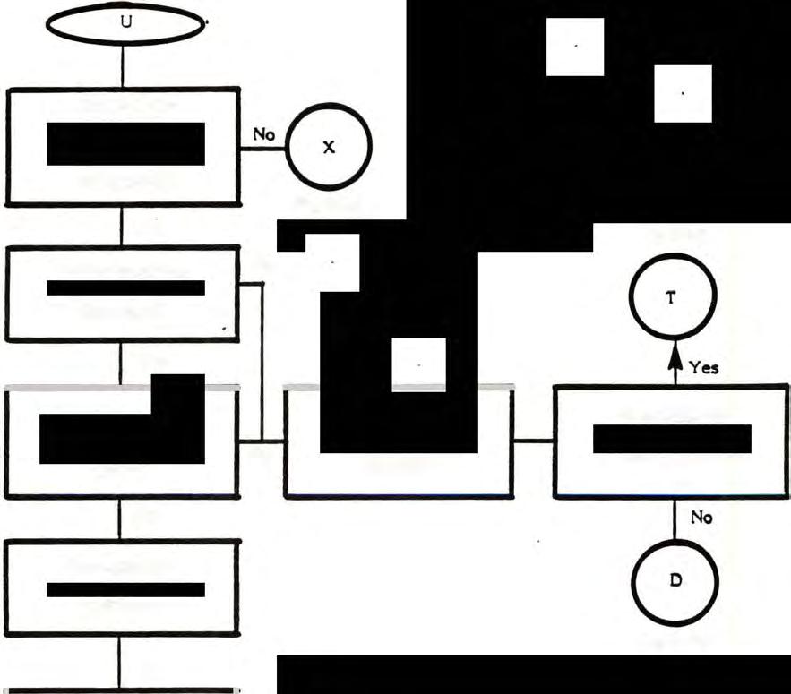
Do the patterns alternate with the tones? Yes
Are both colors and tones consistent each cycle? Yes
Put switches b&cI< to initialized positions.
2600A Audio Test Procedure (Continued)
Are patterns now COlTect? (As in Figure 4-9)
ves will go through one last cycle before changing to color bar test.
6-27 Pg. 6-24 No Swapout 1) A20I 2) A200 3) A202 No 6-21· Pg. 6-20
Pg.
4-45 2600/2600A
Changed per ECN 110021 1/29/83
Pg.
Domestic VCS
2600A Defective I/O Lines Troubleshooting Procedure
Defective ,.\202 Cap. Connector Determine (RAM) 1.ine No. No. Pin No. which lines are lj CEo J202-'Pin � defective by I� C22,) J202·Pln ) referring to lJ e22a J202·Pln 2 Figure�7. 12 C227 J202·Pln I
II C226 J203·Pln � 10 C22' J203.PIn ) ') C22. J203·Pln 2 Check the tines & C223 J203·Pln I indicated as defective for •�v at J202 or J20) (See chart).

Does Diagnostic Is.� present Yes Swapout Yes il A202 Matrix now look on the tine(s) I- 2) A200 t-- correct(Seejust checked? ) A201 Fi�re 11-6or�71?
Checkthe RAM Yes Rf!!)&ir open trace Repair tine (A202)pin. Is +.5v t- between A202 pin
shorted to +'v t-present there? and the J203/3203. (Check trace lines).
Na
Check trace tine(s) from defective pin(s) Yes Repair for shortS toground. Are there any shortS?
SIIIapout A202.
Is .'v now Yes presentat the A202 pin? INo
Replace the capacitor on that tine (seechart).
Does the Diagnostic :-10 Swapout .lIIatrix screen now t-- I) A200 ook correct (see Fig. 11-6) 2) A201 I I P�.6·2

c
T
v �
I
I
INo INo
�
I
INo
I
I
6-22
VC
2600/2600A Domestic
2600A Trigger Line Troubleshooting Procedure C
l) A201 Does trigger line work No R223 or R226 is shorted H Replace I Is there +�v at pin 6 of �
Swapout Yes
2) A200 I-- proper1y now? - to +�v. 3102 (Left Trigger) or

3) A202 J203 (Right Trigger)?
Yes
Are R226 (Left Trigger) No Replace I-- defective resistor. R223 (Right Trigger) good and connect to .�v?
Yes
Check continuitybetween 9-Pins (J202 c!c 3103) and resistors (R22� and R224). I
Continuity good? .�o Repair Trace I-IYes
Open R224, R22� or shorted C216, C217.
Replace I
Pg. 6-2
'11 ::> 1
INa
I
t
-r
6-23 2600/2600A Domestic Vc.
Is RF moduletuned to 61.2' MHz?
(Channel3)
Yes
Is only one audio tone present? No
Is there a 2v p-psquare wave thatalternates between two trequencies on pin 13 ot A20l? Yes
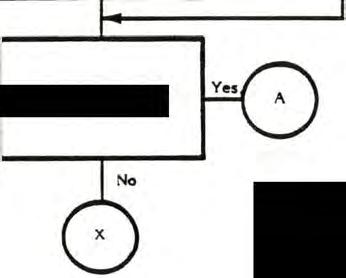
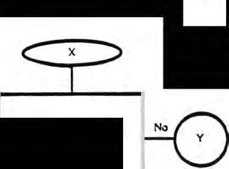
Does square wave signal appear at C20ll? No
Fix open trace line between C20ll and Pin 12/13 ot A201.
2600A Audio Troubleshooting
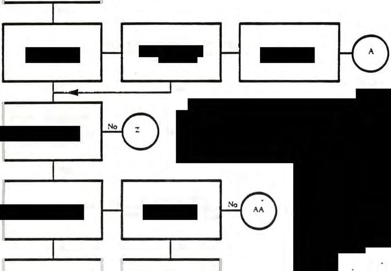
Ps- 6-2'
Yes Is there adetective A201 Yes Repair or open A201 pin 12 and A201 pin 13?
No
Pg. 6-2'
Yes Is there a 4.' MHz, modulated, 1-2v p-paudio
Pg. 6-26 signalat C211 (either side)
Yes Replace
1) C211
2) R207
Is there nowan alternatingaudiotone trom the TV?
Pg. 6-2
Pg. 6-2
6-24 2600/2600A Domestic ves
2600A Audio Troubleshooting (Continued)
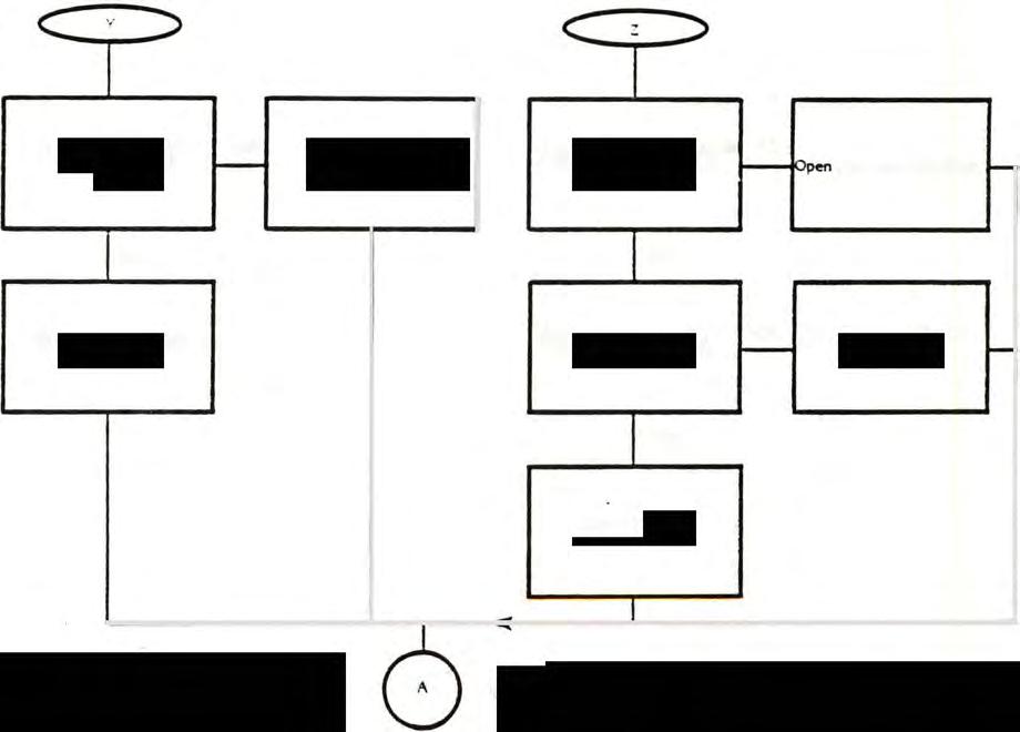
Can RF module be Yes
Is., present at the side of No pt'operly tuned? - Tune RF module. R206 closest to L20I? f---Open between .,de R206 "No
Yes
Is there continuity from No Repair open betw""n Replace RF module. R206 to A201 pin 13? f- R206 and A20I � pin 13.
Yes
Swapout A201.
" . ..,
c::::
c::::
v ::>
::: :::> 1
I
1
T 6
6-25 2600/2600A Domestic VCS
2600A Audio Troubleshooting (Continued)
Fix open trace tine between aoa and Pin 12113ot IUO!.
Is tllere •�v at one �d ot1.20I?
�e!l&ir trace fr-om ·5". :0 1.201.
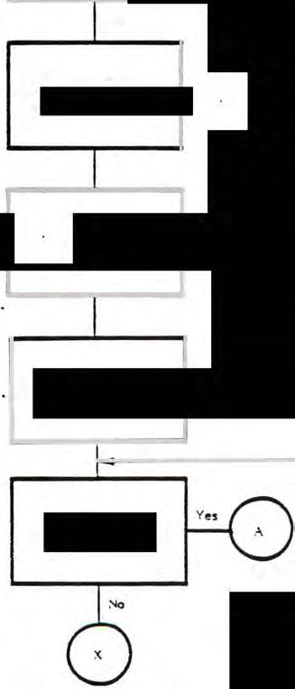
Yes
Check tI\at 1.20IisI\ood. (Hu COfttlnuitv and IS nOt sllorted or Cracked.l

ChecklReolace II C200,C207
2)1.201 ) 1.202
If audio is still dead. ChecK tile trace lines around C21i !or opens and sIIons.
Is tllere no", an alternatin� audio tone from tile TV?
P�.6·2
Pg.6·24
6-26
2600/2600A Domestic VC
DTC works, but YCS unit is still suspect.
2600A Cartridge Test Procedure
Plug in C-lstomer cartridge, if available.
Available
Connect, initialize, and tum yeS on with customer's game cartridge.
Does correct video pattern for that game appear? Yes
Play game. Does it play OK?
Check customer cartridge on known good game. Is it OK?
Replace with good cartridge.
Does game now operate properly with game cartridge?
No
No
Pg. 6-28
Pg. 6-28 No Pg. 6-28 Swapout
1) A201 2) A200 3) A202 6-27
Not Available
Yes
Pg. 4-45 2600/2600A Domestic VCS
2600A Burn-� Procedure
Place customer cartridge in game, if available. Otherwise, use other game cartridge. Run came for 2 hours, minimum. Do "ot tum off duringthis period.
Checl< game's operation.
15 game working properly?
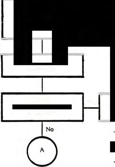
Pg. 6-2 Yes 6-28 End of .test sequence. 2600/2600A Domestic yeS
2600A Paddle Lines Test C Start :::>
Put shorting plugs in. Put YCS into Diagnostic Matrix mode. I I
Check 3202/3203 for RC
Does waveform appear at Repair open waveform (see Fig. �-IO). Yes No trace between Is waveform present on t-- each ot the A201 pins � A20I and 1202/ each of the pins shown shown in the chart? J203. in chart? No Yes
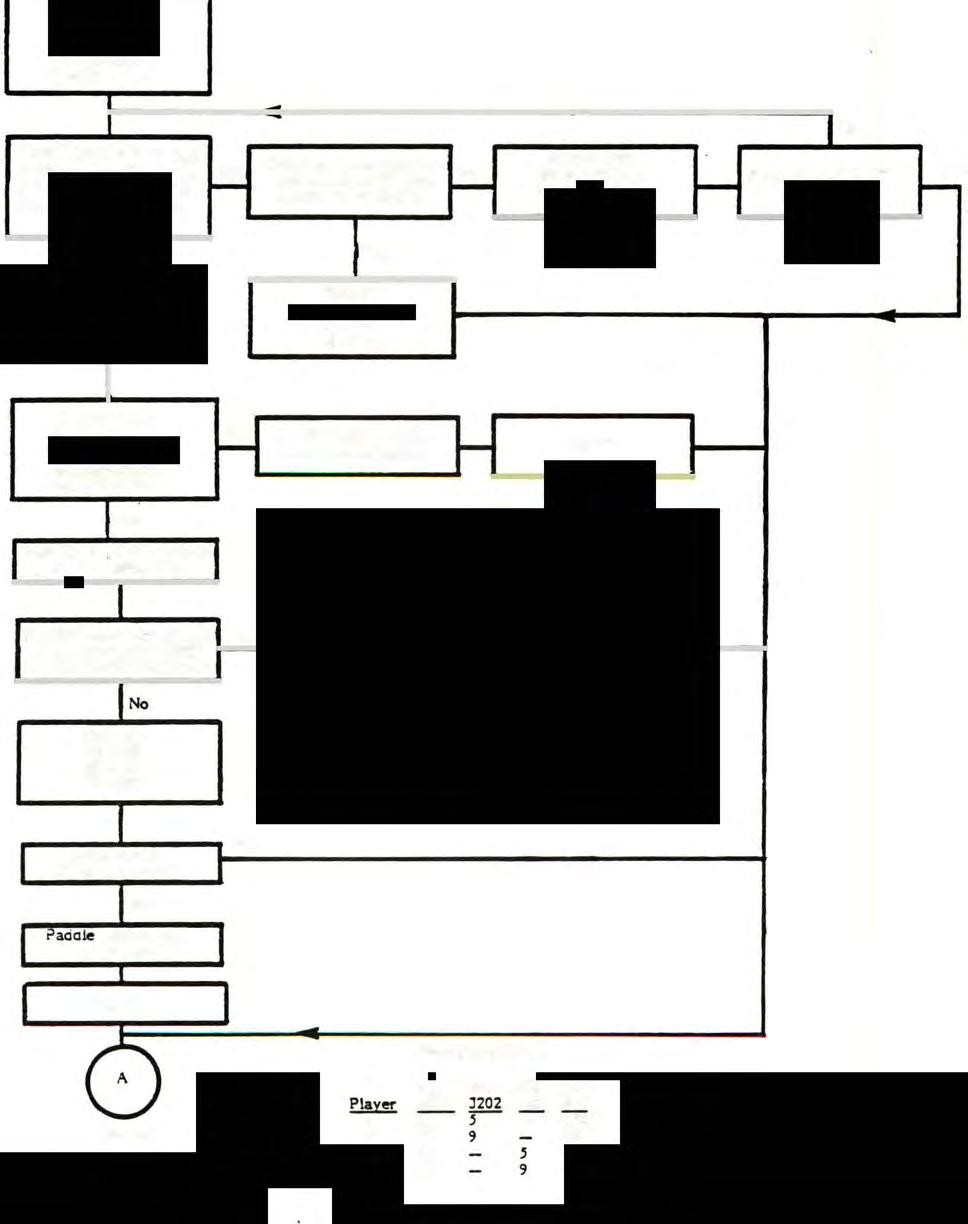
Swapout
1) A201
2) A200
3) A202
Is there continuity between No Check trace lines and Repair the 1202 or 1203 � resistors for opens. 100pin (seechart) and the A20 I? Yes
Replace cap (C21.5-C218) on the failed line. I
DQes RC waveform appear Yes on the appropriate J202 or 1203 line? (SeeOlart) I No
Swapout
I) A201
2) A200
3) A202 I
Does Paddle Line now work? I No
?aciale line isopen or shorted. I r R"pair 0

Yes J I
I No
Do paddle lines now Yes � work OK? "'--
Pg. 6-2
Player 1 2 3 � Connection Chart Pin A20 1 40 39 38 37 Pin lill 6-29 Pin 203Cap No. C21.5 C216 C217 C218
2600/2600A Domestic ves
SECTION 7 GAME CONTROLLERS
OVERVIEW
The following pages contain descriptions, schematics, and test procedures for the four game controllers used with the Video Computer System.
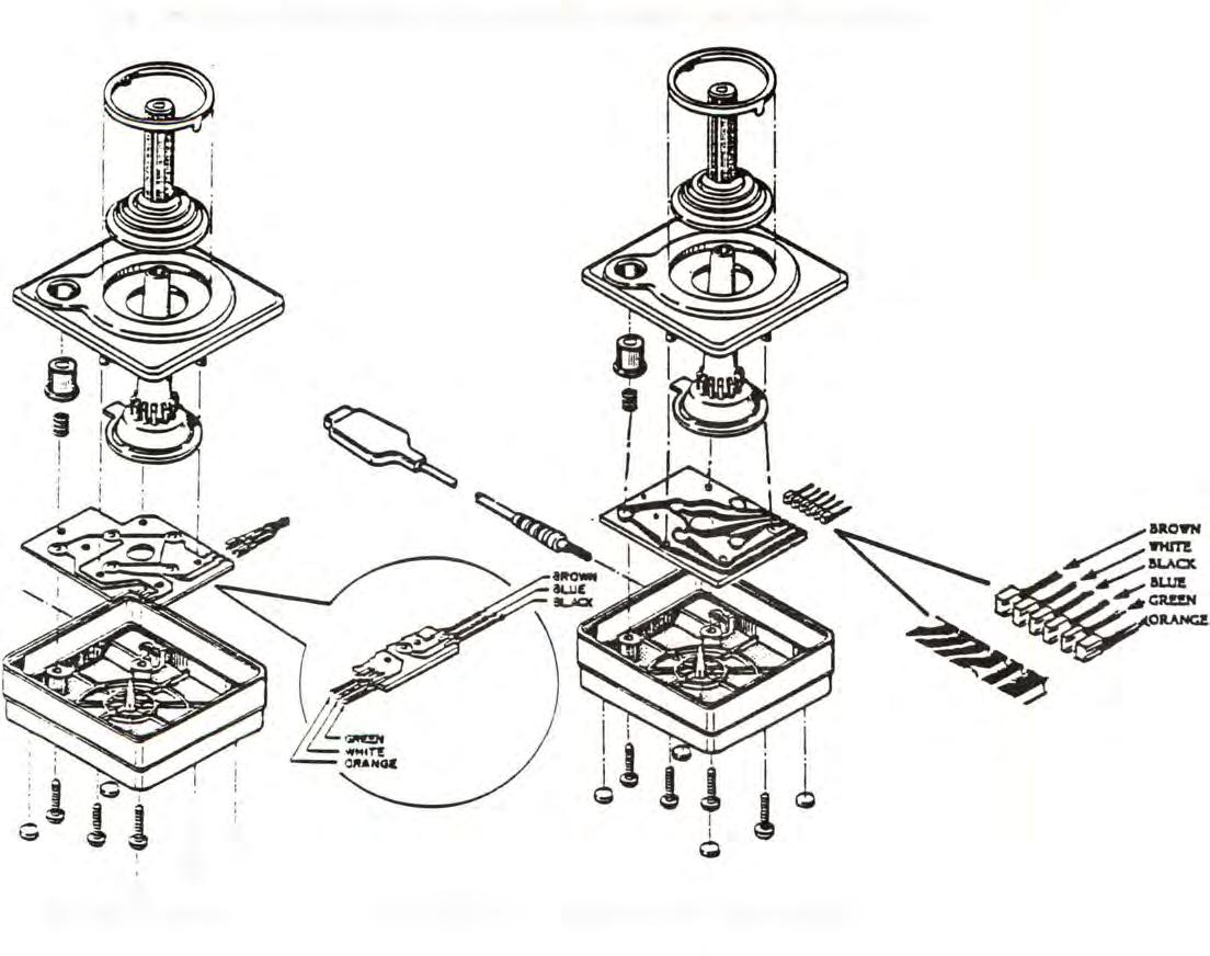
JOYSTICK <X-Y) CONTROLLER

Inside each joystick is a small PC board that has five calculator-type keypads mounted on it. Two versions of the PC board exist in current joystick models; see Figure 7-1. Four of the keypads are positioned beneath the stick in a square shaped pattern, and the fifth is located beneath the pushbutton. When the stick is pushed forward, the bottom surface of the stick presses against the forward keypad, causing it to make contact, and co ' mplete the circuit that is connected to it. In the same way, pushing the stick back, left and right causes the respective keypad underneath that position to close and complete the circuit.
NOTE: The earliest models of the joystick had five spring-loaded buttons instead of �e present configurations. These earlier models cannot be repaired.
I ! Q o Earlier Version Figure 7-1.
Contr?llers 7-1 2600/2600A Domestic ves
Joystick (X-Y)
If the stick is pushed forward and to the right at the same time (that is, in a northeastern direction), both the forward and right keypad close simultaneously, which causes the 6532 to see two switch closures happening at once. The result is that the object being controlled on the screen moves diagonally. With the four keypads, 8 different directions can be attained. The pushbutton determines whether the keypad beneath it is either open or closed. See Figure 7-2 for Joystick Schematics. @inII

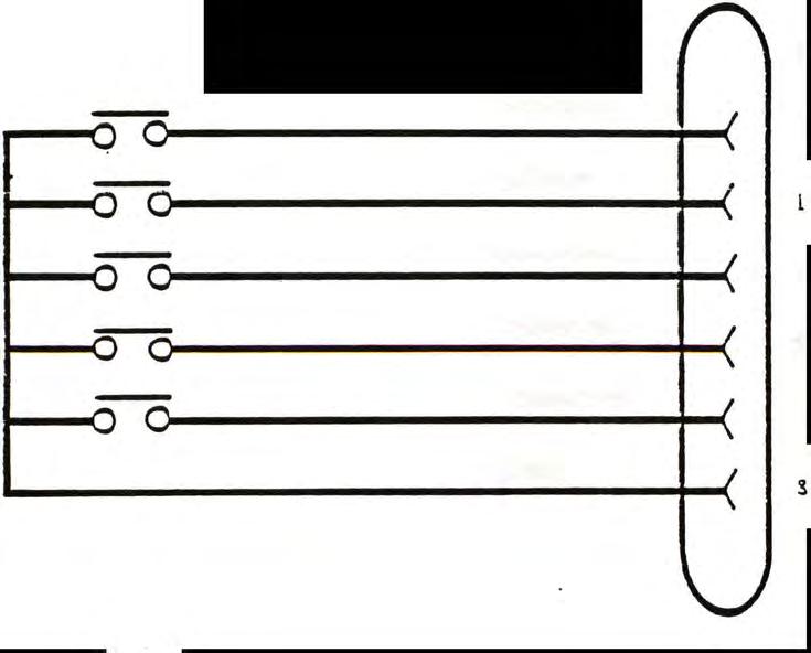

Fire/Oran�e G Up/White Down/Blue 2 Left/Green 3 Right/Brown 4Blad<
7-2
Figure 7-2. Joystick Schematic
2600/2600A Domestic yeS
JOYSTICK (X-Y CONTROLLER) CHECK
Equioment 0ieeded
• T.V. set
• Known good VCS unit
• Combat cartridge
Procedure
1. Check for cosmetic damage.
2. Plug in cartridge and plug controller to bete'5ted into the left Dlayer port.
3. Turn on unit and press GAME SELECT until game 1113 appears.
4. Press GA\t\E RESET.
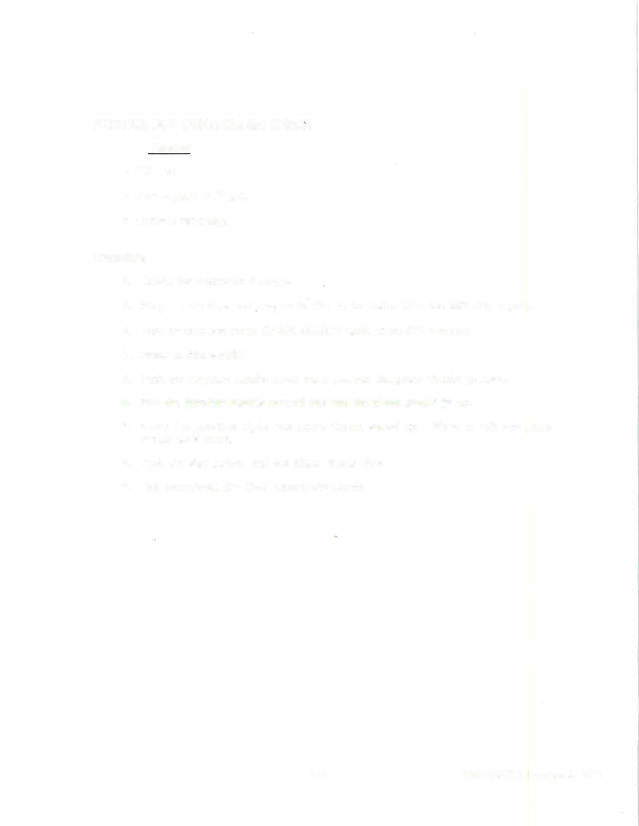
5. Push the joystick handle away from you and the plane should go down.
6. P ullthejoystickhandletowardyou and the plane should go up.
7. \'love the joystick right and plane should soeed up. �'\ove it left and plane should slow down.
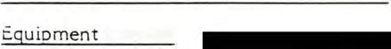
3. Push the Red button and the plane should fire.
9. This completes the (X-Y controller) check.
7-3 2600/2600.'\ Domestic ves
P,'\DDLE CONTROLLER

Each game paddle consists of a 1 Megohm potentiometer that, when varied, causes different values to be seen and acted upon by the TlA. Also contained in the paddle is a' simple spring loaded push-to-make pushbutton switch. There are two game paddles connected to each I/O plug. Figure 7-3 illustrates the paddle controller assembly and Figure 7-4 the paddle controller schematic.
, I , I !
Figure 7-3. Paddle Controller 7-4
2600/2600A Domestic YCS
..J::L BUTTON CONTROL I 0 POT I
V� 5 VOLTS GND "
.n... BUTTON CONTROL 2 (' 0 POT2
'A:c5 VOLTS GND
P:\DDLE CONTROLLER CHECK
Eauioment Needed
• T.V. Set
• Known good VCS unit
Ny" CABLE DUAL 4 CONDUCTOR
GREEN VIOLET
yaLOW BLACK 'I" ;, BROWN RED y
COlOSI � / , "'
o PIN 3
PIN 9 PIN 7 PINS
PIN 4
PIN 5
C T\1 'd
• aSlnO cartn ge
Procedure
1. Check for cosmetic damage.
2. Plug in cartridge and plug controllers to be tested into the left player port.
3. Press game reset.
4. Press the button on one of the controllers. ,-\ oair of numbers should appear.
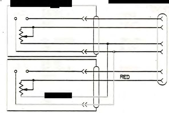
5. When you turn the knob, one set of numbers should �o between 20 and 200 by steps of 20. The numbers should not advance greater than a step of 20.
6. Repeat steps 3, 4, .x 5 for the other controller.
(/ 1
�
�
Fi�ure 7-4. Paddle Controller Schemat:c
7-5 2600/2600A Domestic VCS
DRIYI�G CONTROLLER

The heart of the driving controller is a switching device that generates a full two-bit gray code for each quarter turn of the controller knob. The output of both the gray code generator and the pushbutton switch is detected by the 6532, causing the program to respond accordingly. Unlike the non-linear resistive game paddles, the driving controller gives the user precise linear positional control over the complete turning range of the knob. As with the game paddles, there is a simple push-to-make pushbutton switch located on the side of the controller. The driving controller assembly is illustrated in Figure 7-5; the sc'·-:: ,�C11:ic in Figure 7-6.
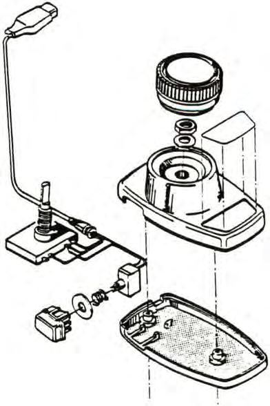
I I , I i �
7-6 2600/2600A Domestic YCS
Figure 7-5. Driving Controller
DRIVING CONTROLLER CHECK
Eguioment Needed
• T.V. set
• Known good VCS unit

• Indy 500 cartridge
Procedure
1. Plug in Indy 500 cartridge and plug in driving controller to be tested in left hand port.
2. Press game reset switch.
3. Turn controller knob and insure that car turns in the same direction as the knob. Insure that car doesn't skip position or wobble between positions. There should be 16 different positions for the car.
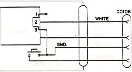
4. Press down on the knob and lightly wiggle it back and forth. The car should not move at all.
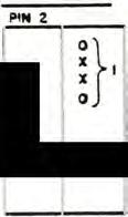
5. Press down on the red button. The car should move forward.
6. Ifthecontrollerfailsanyoftheabovetestsitisdefective.
TRUTHTABLE A Pi"2 1'1"4 CO�24 o o lC lC 2lilTGlu:rCOOE C1.OCXWISI
lC.NO
OGNO COI0802 4 GHO. ?o�U ACC£URATOR NOn: WHiT£ BLUE BL.ACX ORANGE Y .... PINI ""N2 PINS PlN6 I.
ReTAnO"
CONN(CTlCN
0CClJfIS
.4 Tll11U PO REV. I.1'1" I_3-'REl"nllNALL.TCONNlrTm ONCOIoe02
Figure 7-6. Drivin� Controller Schematic
7-7 2600/2600A Domestic VCS
KEYBOARD CONTROLLER
The keyboard controller (Figure 7-7) is a 12 button calculator-type switch array that functions like a small computer keyboard. When one of the pushbuttons is pressed, the corresponding set of sense lines is closed, completing the circuit. The closure is detected by the 6532 and appropriate action is taken by the program. Figure 7-8 illustrates the keyboard wiring and Figure 7-9 the keyboard schematic.
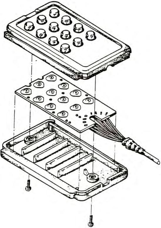 Figure 7-7. Keyboard Controller 7-8
2600/2600A Domestic VCS
Figure 7-7. Keyboard Controller 7-8
2600/2600A Domestic VCS

SI 54 S7 SlO
r-f'"?Y"?R302 ••71( R30I .-:7X52Y----53Y - 5!5 -v--56Y --58Y-v--S9! ...-?�5111 ---sI21-CONm:lU..ER t VIOLET G� WHIT[ GRAY BROWN RED ORANGE YELLOW SLUE CAa.£
Figure 7-8. Keyl)oard Wiring Diagram
7-9 r-'-PIN7 PINS PlN9 PlN8 PINI PIN2 PlN3 PlN4 PIN6 ��� 51 •I' 52 •Z" S3 •3" S<4 '." S5 '5· 51 '," ST '7" SI ·s· D ',. SIO '.' 511 '0" SIZ '.. 2600/2600A Domestic yeS
Figure 7-9. Keyboard Schematic
KEYBOARD CONTROLLER CHECK
Equipment Needed
• T.Y. set
• Known good YCS unit

• Brain Games cartridge
• One good keyboard controller
Procedure
1. Check for cosmetic damage.
2. Plug in Brain Games cartride;e and plug; the known good keyboard into the right-hand plug.
3. Plug the controller to be tested into the left-hand plug.
4. Press game select until game 1119 appears and press game reset.
5. If an audio tone sounds, the controller is defective.
6. Starting with the "1" key, press the keys in the following order: 1, 2, 3, 4, 5, 6, 7, 8, 9, *, 0, II. Each key should generate a tone lower than the key before it.
7. Test completed.
7-10 2600/2600A Domestic yeS
SECTION 8

CX2600 DOMESTIC (MIN) ves PARTS LIST
� Part No. Description Locator Bezel CA010873 Bezel Assy Console 88-1004 RubberFeet Console C010307-01 Console Top Console C011925 Console Base Console CAOI0869 Console Base Assy Final C016353 AC Power Adaptor Not Packaged Final CA010112 TV Switch Box Not Packaged Final CA010800 CX2600 VCS Not packaged Final CA012758-01 Keyboard Controller Packaged Final CA012759-03 Driving Controller Packaged Final CA012760-06 Paddle Controller Packaged Final CAO12994-03 X-Y Controller Packaged Final CA014034 AC Power Adaptor Packaged (Alternate listed) Final CA018200-01 AC Power Adaptor Packaged (Alternate for PIN CA014034) Final CA018201-01 TV Switch Box Packaged (CX262 Pack) Mother 14-5101 Resistor 1/4W100 Ohm R202,205 Mother 14-5102 Resistor 1/4W1K R208,212,214 Mother 14-5103 Resistor 1/4W10K R225,226,234 Mother 14-5123 Resistor 1/4W12K R222 Mother 14-5182 Resistor 1/4W1800 Ohm R203,216,227-321 Mother 14-5183 Resistor 1/4W18K R209,233 Mother 14-5221 Resistor 1/4W220 Ohm R204 Mother 14-5243 Resistor 1/4W24K R206,217,223 Mother 14-5270 Resistor 1/4W27 Ohm R200 Mother 14-5332 Resistor 1/4W3300 Ohm R218-221 Mother 14-5471 Resistor 1/4W470 Ohm R201 Mother 14-5472 Resistor 1/4W4700 Ohm R207,232 Mother 14-5473 Resistor 1/4W47K R224 Mother 14-5681 Resistor 1/4W680 Ohm R213 Mother 14-5682 Resistor 1/4W6800 Ohm R215 Mother 14-5912 Resistor 1/4W9100 Ohm R210 Mother 19-411504 ResistorVariable 500K R211 Mother 21-101104M Cap. Mylar Dipped .luF (lOOV) C204 Mother 2A-008 Cap. CeramicDisc47pF (50V) C211,212 Mother 2A-018 Cap. CeramicDisc22pF (50V) C213 Mother 2B-004 Cap. CeramicDisc 220pF (50V) C236,237 (Alternate for PIN C014180-05) Mother 2B-007 Cap. Ceramic Disc. 01uF (50V) C200,202,205,208, 214,223-227,239,240 8-1 2600/2600A DomesticVCS
CX2600 DOMESTIC (MIN) VCS
PARTS LIST (Continued)
� Part No. Description Locator
Mother 2B-008 Cap. Ceramic Disc .001uF (50V) C203,209,222,228235,238
Mother 2B-009 Cap. Ceramic Disc l50pF (50V) C22l
Mother 2C-001 Cap. Ceramic Disc. 1uF (50V) C2l0,2l9,220
Mother 3l-lN9l4 Diode lN9l4 CR200,201
Mother 33-2N3906 Transistor2N3906 Q200,20l
Mother 34-2N3563 Transistor2N3563 Q202 (Alternate Listed)
Mother 34-MPS3563 Transistor MPS3563 Q202 (Alternate for PIN 34-2N3563)
Mother 79-5918 Jack J204
Mother CAOl0434 CX2600 PC Board
Mother CAOl0808 Cartridge Socket Assy J200
Mother CA018263 Zener Diode/Axial Wrap Assy
Mother COlOln Crystal 3.579575 Mhz X200 (Alternate Listed)
Mother COl03l4 Socket Cartridge
Mother COl0336 Cap. Electrolytic 4.7uF (35V) C20l
Mother COI0444 IC TIA A201
Mother COl0448 Socket Controller(9 Pin) J202,203 (Alternate Listed)
Mother COI0727 Socket Controller(9 Pin) J202,203(Alternate for PIN COI0448)
Mother COI0745 IC CPU (6507) A200
Mother COI0750 IC RAM (6532) A202
Mother COlOn6 Dust CoverSocket
Mother COI0806 Connector(12/24) J200
Mother COI08"12 Pad Cartridge Socket
Mother COl08l6 IC Hex Buffer(4050B) A203
Mother COI0821 Cap. Polystyrene 820pF (50V) C206,207
Mother COI0822 Inductor2uF L202
Mother COI0823 Inductor 12 1/2 Turn L201
Mother COI0887 Socket Assy (AID)
Mother C012776 Cable Ribbon (12 conductor)
Mother C014180-05 Cap. Axial 200pF (50V) C236,237 (Alternate listed)
Mother C014353 Cap. Epoxy Dipped .068uF (100V) C215-218
Mother C014384 Ferrite Bead L200,203
Mother C014386-08 Socket IC (28 Pin) A200
Mother C014386-09 Socket IC (40 Pin) A201 ,202
Mother C015510 Crystal 3.57957.5 Mhz X200 (Alternate for PIN COIOl77)
Mother C016035 Rivet
Mother C017654 Diode Zener 1N4736 (6.2V)
CR202,203
Mother C018991 Transistor2N3906 Q200,201
Mother CAOI0434 CX2600 PC Board (MOTHER)
2600/2600A Domestic VCS
8-2
.
Assy Part No.
Mother CAOI0798
Mother CAOI0808
Mother CA018263
Paddle 81-4004
Paddle C010416
Paddle C010417
Paddle C010457
Paddle C010464
Paddle C010737
Paddle C010738
Paddle C010739
Paddle C010810
Paddle COI0970
Paddle C012766
Paddle CA010837
Paddle CA010933
Paddle CAOI0953-03
Paddle CAO11620-01
Switch 13-5680
Switch 21-101224M
Switch 2B-007
Switch 78-06019
Switch 79-5903
Switch C010301-05
Switch C010373
Switch C010388

Switch C010813
Switch C010820
Switch C01l695
Switch C012241
Switch C012242
Switch C014348
Switch C014372
Switch C014373
Switch C014778-03
Switch C017294
Switch COl7297
Switch C019025
CX2600 DOMESTIC (MIN) ves
PARTS LIST (Continued)
Description
Electronic Module Assy
Cartridge Socket Assy
Zener Diode/Axial Wrap Assy
Speed Clip Fastener
Nut
Lockwasher
Knob
Resistor Variable I Meg
Top Cover
Bottom Cover
Fire Button
Cable Y Control
Sleeve
Paddle Label
Control Knob Assy
Control Cable Assy
Paddle Control Assy
Switch
Resistor 2\v 680 Ohm
Cap. Poly Film .22uF (100V)
Cap. Ceramic Disc .01uF (50V)
Heat Sink
Socket Phono
Jumper (llAWG)
Switch Slide
Switch DPST - Spring Return
Switch Dust Cover
Inductor 15uH
Heat Sink
Switch SPOT
Switch SPOT
Regulator 78M05 (TO-220)
Cap. Electrolytic 4.7uF (35V)
Cap. Elect Axial 2200uF (16V)
Socket (12 Pin in-line)
3 Switch Static Strip
2 Switch Static Strip
Switch Slide
Locator

J200
CR202, 203
R101 (Ch 3 version) C103,104 CIOl,102 (Ch 3 version) J102
5101-104 (Alternate listed)
5105,106 (Alternate listed)
L101,102 (Ch 2-3 version) 5107 (Alternate listed)

5107 (Alternate for PIN C012241) listed) AlOl C105 C106 J101
5101-104 (Alternate for PIN COI0373)
2600/2600A Domestic VCS
8-3
Changed per ECN 110021 1/?Q/'J.?'
•
Assy Part No.
CX2600 DOMESTIC (MIN) ves
PARTS LIST (Continued)
Description Locator

Switch C019026 Switch DPST S105,106 (Alternate for PIN C010388)
Switch CAOl2174 RF Module Assy 5 Pin (Ch 2-3 version)
Switch CA012175 RF Module Assy 3 Pin (Ch 3 version)
Switch CA012233 PC Board Assy (Switch)
x-Y Cntl C010726 Cable
X-V Cntl C012107-02 Top Cover

X-V Cntl C012108-02 Bottom Case
X-Y Cntl C012109 Boot
X-V Cntl C012110 Retainer Ring
X-V Cntl C012114 Fire Button
X-V Cntl C012116 Handle
X-V Cntl C012951 Spring
X-V Cntl CA015396 PC Board (Two-Edged Connection)
X-V Cntl CA016741 PC Board (Single-Edge Connection)
•
8-4 2600/2600A Domestic VCS
CX2600A DOMESTIC (MIN) VCS
PARTS LIST


� Part No. Description Locator
C015572 Bezel
C015901 Bezel Label
CAO15908-01 Bezel Assy Console 88-1004 Rubber Feet Console C015570 Console Top Console C016398 Console Base (Alternate listed) Console C016398-01 Console Base (Alternate for PIN C016398)
CAO15909-01 Console Base Assy
C016353 AC Power Adaptor (Not Packaged)
CAOI0112 TV Switch Box (Not Packaged) Final CA012758-01 Keyboard Controller (Packaged) Final CA012759-03 Driving Controller (Packaged) Final CA012760-06 Paddle Controller (Packaged) Final CAO12994-03 X-Y Controller (Packaged) Final CA014034 AC Power Adaptor Packaged (Alternate listed)
CA015799 CX2600A VCS (Packaged)
CA015907 CX2600A ves (Not packaged) Final CA018200-01 AC Power Adaptor Packaged (Alternate for PIN CA014034) Final CA018201-01 TV Switch Box Packaged (CX262 Pack) Mother 14-5102 Resistor 1/4W lK R202,206,211,228 Mother 14-5103 Resistor 1/4W 10K R223,226,229,230 Mother 14-5114 Resistor 1/4W 110K R216 Mother 14-5153 Resistor 1/4W 15K R222 Mother 14-5182 Resistor 1/4W 1.8K R209 Mother 14-5183 Resistor 1/4W 18K R207 Mother 14-5221 Resistor 14W 220 Ohm R204,224,225,232 Mother 14-5222 Resistor 1/4W 2.2K R203 Mother 14-5241 Resistor 1/4W 240 Ohm R205 Mother 14-5243 Resistor 1/4W 24K R217,227 Mother 14-5273 Resistor 1/4W 27K R214 Mother 14-5332 Resistor 1/4W 3300 Ohm R218,220 Mother 14-5472 Resistor 1/4W 4.7K R201,212,219,221 Mother 14-5473 Resistor 1/4W 47 Ohm R215 Mother 14-5474 Resistor 1/4W 470K R233 Mother 14-5682 Resistor 1/4W 6800 Ohm R210 Mother 14-5821 Resistor 1/4W 820 Ohm R234 Mother 14-5910 Resistor 1/4W 91 Ohm R231 Mother 14-5912 Resistor 1/4W 9100 Ohm R208 Mother 19-411504 Resistor Variable 500K R2 13 Mother 21-101104 Cap. Poly Film .luF (lOOV) C241 Mother 21-101224M Cap. Poly Film .22uF (lOOV) C204 Mother 2A-003 Cap. Ceramic Disc 10pF (50V) C202 (Alternate listed) 8-5 2600/2600A Domestic VCS
Bezel
Bezel
Bezel
Console
FinaJ
Final
Final
Final
Assy Part No.


CX2600A DOMESTIC (MIN) VCS
PARTS LIST (Continued)
Description Locator
Mother 2A-008 Cap. Ceramic Disc 47pF (50V) C209,2l0
Mother 2A-018 Cap. Ceramic Axial 22pF (50V) C2l! (Alternate listed)
Mother 2B-003 Cap. Ceramic Disc 470pF (50V) C2l6,2l7 (Alternate listed)
Mother 2B-007 Cap. Ceramic Disc .OluF (50V) C203,205,2l2,236, 237,240,244 (Alternate listed)
Mother 2B-008 Cap. Ceramic Disc .001uF (50V) C213,223-235 (Alternate listed)
Mother 2B-009 Cap. Ceramic Disc l50pF (50V) C215 (AIternate listed)
Mother 2C-001 Cap. Ceramic Disc .1uF (50V) C200,208,222,238, 239,245 (Alternate listed)
Mother 31-lN914 Diode lN9l4 CR200-203
Mother 34-2N3563 Transistor 2N3563 Q202
Mother 79-5903 Connector Phono Jack J204
Mother 79-5918 Connector Jack (3.5mm) J20l
Mother A003647 RF Cable Assy
Mother COlOl77 Crystal 3.579575 Mhz X200 (Alternate for PIN C0155l0)
Mother COl0373 Switch Slide (DPDT) S20l,204
Mother COl0388 Switch Slide (DP Spring Return) S202,203
Mother COl0444 IC TIA A20l
Mother COI0448 Socket Controller (9 Pin) J202,203 (Alternate listed)
Mother COl0727 Socket Controller (9 Pin) J202,203 (Alternate for PIN COl0448)
Mother COl0745 IC MPU (6507) A200
Mother COI0750 IC (6532) A202
Mother COl0776 Dust Cover Socket J200 (Part of)
Mother COl08l2 Pad Cartridge Socket J200 (Part of)
Mother COl08l3 Dust Cover Used on Switches
Mother COl082l Cap. Polystyrene 820pF (50V) C206,207
Mother COI0823 Inductor Variable 0.85-1.•2uH L20l
Mother C01224l Switch Slide (PCB) S200,205,206
Mother C014l79-0l Cap. Ceramic Axial 22pF (50V) C2l! (Alternate for PIN 2A-018)
Mother C014179-03 Cap. Ceramic Axlal lOpF (50Y) C202 (Alternate for PIN 2A-003)
Mother C014179-05 Cap� Ceramic Axial 47pF (50V) C209,2l0 (Alternate for PIN 2A-008)
Mother C014l80-04 Cap. Ceramic Axial l50pF (50V) C2l5 (Alternate for PIN 28-009)
8-6 2600/2600A Domestic YCS
CX2600A DOMESTIC (MIN) VCS
PARTS LIST (Continued)
Assy Part No.
Mother C014180-07 Cap. Ceramic Axial 470pF (50V) C216,217 (Alternate for PIN 2B-003)
Mother C014181-01 Cap. Ceramic Axial .001uF (25V) C213,223-235 (Alternate for PIN 2B-008)
Mother C014181-02 Cap. Ceramic Axia1 .01uF (25V) C203,205,212,236, 237,240,244 (Alternate for PIN 2B-007)
Mother C014181-03 Cap. Ceramic Axial .1uf (25V) C200,208,222,238, 239,242,245 (Alternate for PIN 2C-00l)
Mother C014348 Voltage Regulator 78M05 (5V) A203
Mother C014353 Cap. Epoxy Dipped .068uF (lOOV) C218-221
Mother C014369 Cap. Elec 4.7uF (35V) C214
Mother C014373 Cap. Elec 2200uF (l6V) C243
Mother C014384 Inductor Ferrite Bead L200,203-205
Mother C014386-08 Socket IC(28Pin) XA200
Mother C014386-09 Socket IC (40 Pin) XA201,202
Mother C015510 Crystal 3.579575 Mhz X200 (Alternate listed)

Mother C015519 PC Board (Use Rev 16 or above)
Mother C015573 Socket Cartridge J200 (Part of)
Mother C015574 Shield Top
Mother C015575 Shield Bottom
Mother C015752 Inductor 1.8uH
Mother C015902 Connector 12/14
Mother C017297 2 Switch Static Strip
(Part of)
Mother C017549 Switch Slide (PCB) S200,205,206, (Alternate for PIN C012241)
Mother C018991 Transistor 2N3906 Q200,201

Mother C019748 IC Timer (555) A205
Mother CA011824 Dust Cover Assy
Mother CA012174 RF Module 5 Pin Version
Mother CA015796 Socket Assy (Cartridge) J200
Mother CA015911 CX2600A PC Board Assy
Mother CA015913-01 PCB/Shield Assy
Mother CA018263 Zener Diode/Axial Wrap Assy
Paddle 81-4004 Speed Clip Fastener
Paddle C010416 Nut
Paddle COI0417 Lockwasher
Paddle C010457 Knob
Paddle C010464 Resistor Variable 1 Meg
Description Locator
L202
J200
8-7 2600/2600A Domestic
Changed per ECN 110021 1/?Q/'!.1
VCS
CX2600A DOMESTIC (MIN) ves
PARTS LIST (Continued)
� Part No. Description Locator

Paddle COI0737 Cover Top
Paddle COI0738 Cover Bottom
Paddle COI0739 Fire Button
Paddle COI0810 Cable Y Control
Paddle COI0970 Sleeve
Paddle COl2766 Label Paddle

Paddle CAOI0837 Control Knob Assy
Paddle CAOI0933 Control Cable Assy
Paddle CAOI0953-03 Paddle Control Assy
Paddle CA011620-01 Switch
X-V Cntl COI0726 Cable
X-V Cntl C012107-02 Cover Top
X-V Cntl C012108-02 Case Bottom
X-V Cnt! COl2109 Boot
X-V Cnt! C012110 Retainer Ring
X-V Cntl C012114 Fire Button
X-V Cntl C012116 Handle
X-V Cntl C012951 Spring
X-V Cntl CAOl5396 PC Board (Two-Edged Connection)
X-V Cnt! CA016741 PC Board (Single-Edge Connection)
8-8 2600/2600A Domestic VCS
•
•
AUDIO TONES
BATTERY ELIMINATOR
BLOCK DIAGRAM

COLOR BAR TEST
CONSOLE
DEFECTIVE RAM PROCEDURES
DIAGNOSTIC FLOWCHART
DIAGNOSTIC MATRIX
DIAGNOSTIC MATRIX TEST
DISPLAY, NO
DRIVING CONTROLLER
GAME PADDLE
GRAY BAR TEST
JOYSTICK
KEYBOARD CONTROLLER
MOTHER BOARD
MPU
OPTION SWITCHES
PADDLE CONTROL LINES
PADDLE CONTROLLER
PADDLE LINES TEST
PARTS LIST
POWER SUPPLY
RAM , DEFECTIVE PROCEDURES
RAM, I/O
RFCABLE RF MODULE
RIBBON CABLE
MODIFICATIONS
SECTION 6 INDEX
STATIC
6-11 3-12, 3A-9, 3C-9 1-2 1-4 3-10, 3A-4, 3C-4 1-1 3A-l, 3C-l 3-3, A-I 3-12 3A-7, 3C-7 3A-3 4-8 4-5 3-11, 3A-5, 3C-5 4-2 4-11 1-2, 2-4, 2-5 1-2 1-2 3-5 4-5 3A-25, 3C-20 5-1 1-2, 2-4, 2-5 3A-1, 3C-l 1-2 1-2 1-2 1-2 3-3 NTSC
SECTION 7
TECHNICAL TIPS
TECH TIP ill
Green J200
On early production 2600's the J200 is green. We found that it is a very unreliable connector after many insertions. This appears to you as a game that sometimes does not work with a cartridge. Replace the connector.
TECH TIP il2
Audio Failures

On Audio Failures the primary suspects are the two polystyrene caps C206/C207. By putting pressure on the sound caps the audio may come on again. Always replace both caps when you replace one.
TECH TIP #3
Kludge

In some of the early production games you notice a inductor and cap over C201 & R206. This was to cure a problem on a cartridge then, but is now no longer needed. Cut the inductor and cap out being careful not to cut the R206 lead.
TECH TIP f/4
Molex Sockets
Chip sockets made by Molex have a low retention value in some cases. This may cause an intermittent color or graphics problem. All sockets with insertion aids should have the insertion aid removed and the chip reinserted.
7-1 NTSC
TECH TIP #5
Floating Ground on 2600
If the ground signal has a lot of noise on it (approx. 1 v.) check continuity on pins 3, 6, and 10 on the JI01.
TECH TIP #6
Left Paddle Failure
Early production 2600 mother boards (Rev 8 and lower) had an artwork error which was corrected by placing a dot over the trace. This insulates the trace from the casting and should always be on the board. The dot is located under the J200 upper left corner, and the trace should be completely covered.

TECH TIP #7
Indy 500
If a unit works on everything except Indy 500 then pin 23 of the A202 is probably shorted to a data line.

TECH TIP #8

Power Jacks
All power jacks should be tested for a snug fit. When the game is on, lightly move power plug in a small circle, if the picture goes off, replace the jack with a new one.
TECH TIP #9
9-Pins
Check all 9-Pin connectors (J202, J203) for pushed or broken pins. Replace all showing problems. 7-2
NTSC
TECH TIP #10
R-220
Check that R220 is properly soldered. If they aren't, they will cause intermittent gray bar problems.
TECH TIP #11
Solder Check
Check solder on the following components: C210, C211, C203, C220, C212, C208, and C209. Long miscues on these caps prevented them from being soldered properly, causing intermittent problems on the board.
TECH TIP #12
Hex Buffers
The 4050 (A203) on the 2600 should be one of the first things checked for any of the following problems: any trigger problem, no Sync., lose of lum lines. This is the reason for a high percentage of returns.

TECH TIP #13
J201 and J101 on the 2600
Both of these connectors should be checked for a good, secure fit.
TECH TIP #14
Crooked Switches
Inspect switches on 2600 switchboard to insure that they set flat and perpendicular to the board. Reset all switches which are not.
7-3 NTSC
TECH TIP fl15


L200 and Chicklets on 2600/2600A
Be sure when assembling the mother board into the casting that the' L200 and chicklets are back under the shroud of the casting.
1".
TECH TIP #16
L201
Make sure the . L201 core has a snug fit or else when 4.5 MHz is set, the core can slip in handling. Also, some 1201 cores be frozen or cracked in the jacket. Replacement is necessary only if the audio carrier frequency cannot be adjusted to 4.5 MHz .
TECH TIP fjl7
Reassembly
When assembling the 2600 mother board into casting make sure C220 and C239 are pushed away from J200 shroud.
TECH TIP /118
Excess Lead Length

Check lead length on model 2600 Taiwan games. Trim excessive lead length on the bottom of the mother board to avoid shorting on casting.
TECH TIP #19
Regulator
On earlyproduction 2600 units with standup regulator and heatsink assemblies, inspect for hairline fractures between the regulator and the switchboard. Also insure that on early domestically produced units the regulator is firmly secured to the heatsink by a tinnerman clip.

7-4 NTSC
Consumer Product Service
Manager of TehnicaJ Support
ATARI� FJELD CHAN;,GE ORDER number__
MODEL: 2600A ATARI Video Computer System
I DATE:
PRIORITY LEVEL:
Mandatory on all 2600As received for service that have 12 volt capacitors in either C241 or C242. Replace all 12V capacitors at C24l and C242 even if no symptoms of failure are apparent.
DIFFICULTY REPORTING:
If yO\,J have any problems or questions concerning the implementation of this Field Change Order, contact the ATARI Tech Line Specialist.
Inside California (800) 672-1466
Outside California (800) 538-1535
)�
\ o--....c_. �
lC192 (3/82)
Consumer Product Service
Manager of TehnicaJ Support
FJELD CHANGE ORDER number 1 A
MODEL.:2600AATARI Video Computer System
DATE: July 19,1982
S
UBJECT:
Changing 12V radial lead capacitors at C24-1 and C24-2.
DESCRIPTION:
Some capacitors for these locations are not rated at an acceptable voltag.e. The incorrect capacitors ·are 12 volt radial lead type (see Figure 1). An easy way to identify a problem at C2l.f.1 or C2l.f.2 is to look at the screen with the diagnostic cartridge running COLOR BAR. The color is very grainy with faint vertical bars. (COLOR BARS look like COLOR SQUARES.)
PARTS:
INSTALLATIONPROCEDURES:
Desolder and remove 2C-001 from C2l.f.l. Insert and solder 21-10110l.f. into C2l.f.1.
Desolder and remove 2C-OOl from C2l.f.2. Insert and solder C014181-03 into C2l.f.2•
Use standard testing procedures as outlined in the 2600/2600A Field Service Manual(COl80l.f.O) •
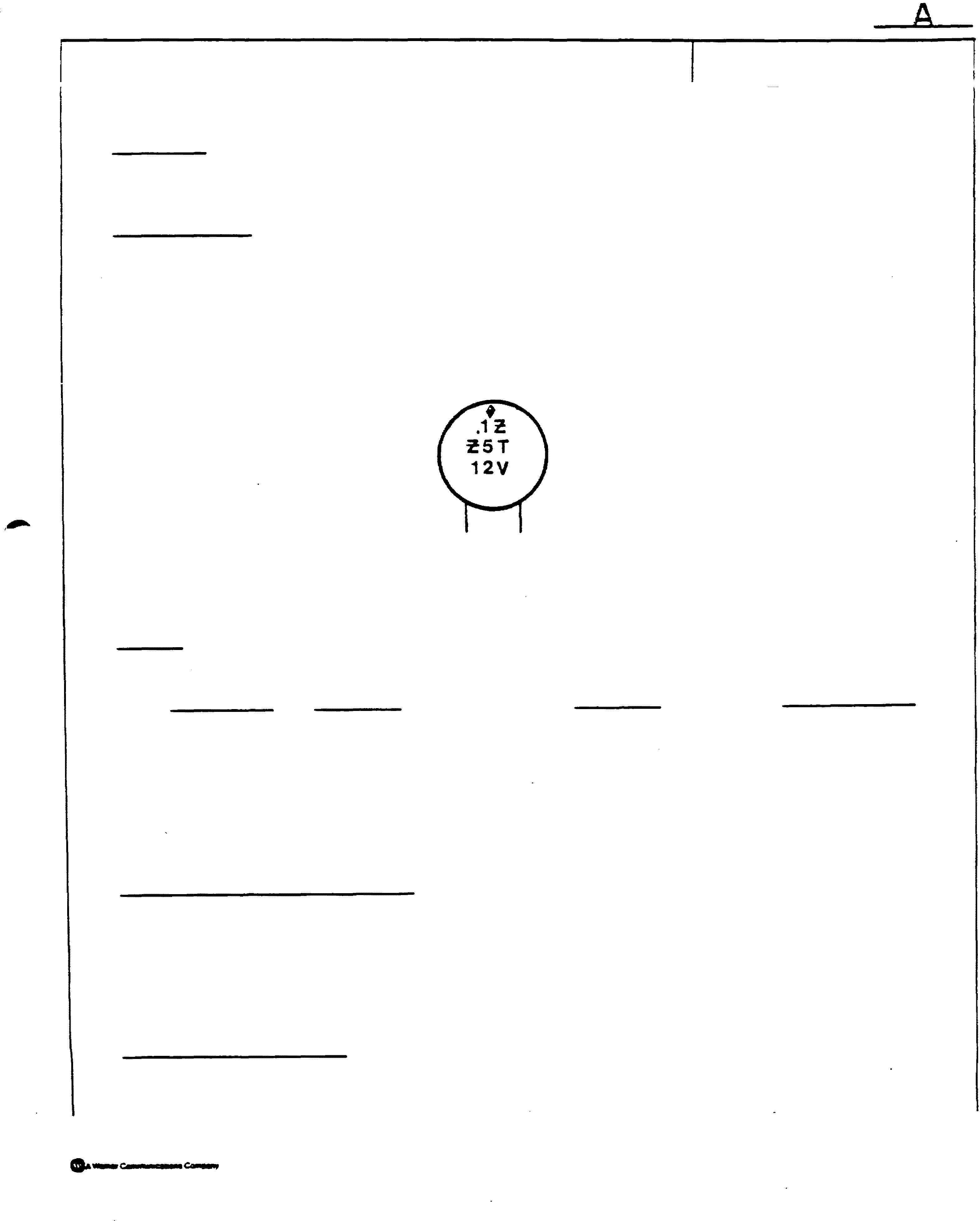
)k ,. ATARI-t
Figure 1. Incorrect C:apacitor
OLD REPLACE PART WITH PART LOCATION NUMBER NUMBER DESCRIPTION C2l.f.l 2C-001 21-101104- .1uf AxialLead Polycap -100v C2l.f.2 2C-001 C01l.f.181-03 .1uf Axial Lead Ceramic - 2.5v
""""TESTINGPROCEDURES:
• lC192 (3/82'
MODEL: CX2800
SUBJECT:
Blanking Resistor
DESCRIPTION:
Consumer Product Service Manager of- Tehnical Support TECH TIP number I


DATE: 11/17/82
The Rev. 4 CX2800 PCB has an 820 Ohm resistor soldered across pins 6 and 9 of U2 (TIA) on the soldered side (bottom). This resistor improves the game color and must not be removed. Rev. 5 and above CX2800 PCB have this resistor incorporated in their design.
DIFFICULTV REPORTING:
If you need further clarification concerning this Tech Tip, call the ATARI Tech-Line Specialist.
Inside California
(800) 672-1466
Outside California
(800) 538-1535
ATARr
lC1tl(3/U)
Consumer Prod uct Service Manager of'
Tehnical Support
MODEL: DATE:
SUBJECT:
5witchcaps
DESCRIPTION:
If at power-up two switches are activated at the same time (indicated by both the Joystick and Paddle, or Novice and Expert LEDls 1I0nll at the same time), you must shorten the switchcap hand ends with sand paper, to eliminate binding.
If the switchcaps seem to be binding when 'activated on Rev. 4 PCBs, tilt the momentary switches (52-59) toward the player port side of the board so that there is a .030 inch gap between the board and the leading edge of the switch bottom (a manual approximation is usually successful). Some Rev. 4 PCBls have a shim glued to the PCB to correct this problem.
DIFFICULTYREPORTING:
If you need further clarification concerning this Tech Tip, call the ATARI Tech-Line Specialist:

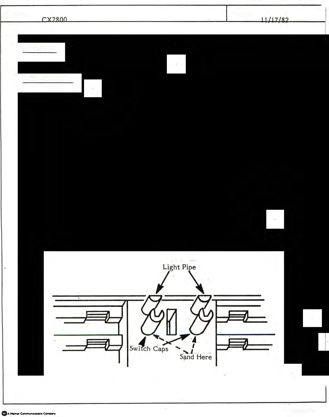
Inside California (800) 672-1466
Outside California (800) 538-1535
ATARI� TECH TIP number -----.,;:3:.:.......-_
le191(3/82)
ATARI�
MODEL: 2600A
SUBJECT:
Blanking Resistor
DESCRIPTION:
Consumer Product Service Manager of' Tehnical Support
TECH TIP number _4-=---_
I DATE: 11/17/9..?
Some 2600A PCBs have an 820 1/4 W 5% resistor (P/N 14-5820 installed on the solder side (bottom). The resistor is located between pins 6 and 9 of A201 (TIA) and improves the color reproduction of the unit.
The resistor may be added to existing 2600A units at your discretion and the customer's expense. The addition wil1 result in improved color saturation.
Rev. 16 PCBs and above will have the resistor incorporated into their design.
DIFFICULTY REPORTING:
If you need further clarification concerning this Tech Tip, call the ATARI Tech-Line Specialist:

Inside California (800) 672-1466
Outside California (800) 538-1535
lClll(3112)
MODEL: CX2800
Cons umer Product Service
Manager of' TehnicaJ Support
TECH TIP number _5=---_
DATE: 11/17/82
SUBJECT: Switch Shortir)g
DESCRIPTION:
The Rev. 4 CX2800 PCB switch S1 (On/Off) has a metal standoff that may short to the trace beneath the switch. To prevent shorting, place a small piece of insulating tape on the board beneath the switch. PCB to Rev. 4 and above have the traces rerouted.
DIFFICULTY REPORTING;
If you need further clarification concerning this Tech Tip, call the ATARI Tech-Line Specialist:


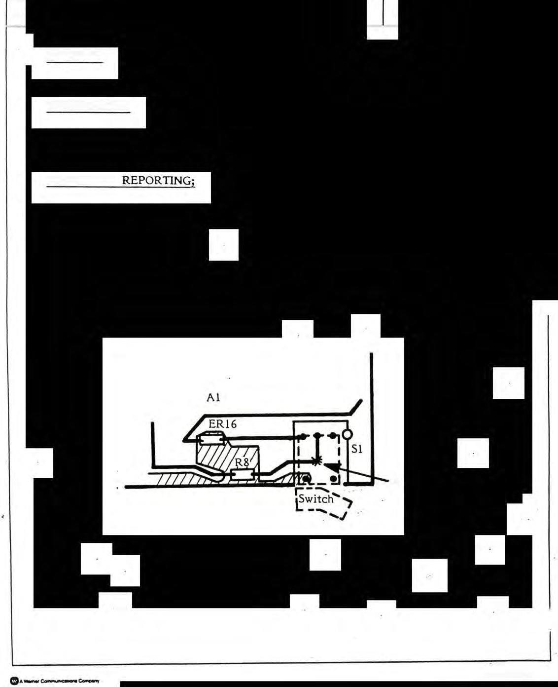
Inside California
(800) 672-1466
Outside California
(800) 538-1535
Metal Standoff
ATA
". ,.
lC191(3/12)
)I� ATARr
ConsumerProductService
ManagerofTechnicalSupport SERVICE BULLETIN
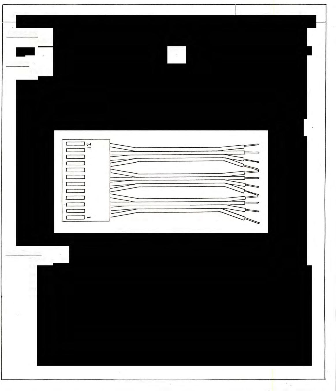
VCS
MODEL: 2600 Video Computer System
PROBLEM
DATE:DEC 9, 1981
Compatability problems between" the cable and connectors linking 2600 Mother Board to the switch board.
CAUSE
Two types of 12-conductor cable assemblies have been used on Model 2600 units:
o
A flat-wire type cable, with female connector (see Figure 8-1) which plugs into a male 12-pin in-line connector on the switch board.
A ribbon cable with a male connector which plugs into a female, 12-pin in-line socket on the switch board.
SOLUTION
When a defect is found in the flat-wire type cable assembly or its male connector on the switch board, the flat-wire cable -assembly should be replaced with the ribbon cable assembly (part number C012776) and the 12-pin male switch board connector should be replaced with�e 12-pin female switch board socket (part number COI4778-03).
o
Figure 8-1. Flat-wire �ype Cable
8-1 1C174(12/81)
Consumer Product Service
VCS Manager of Technical Support
MODEL: 2600A Video Computer System
PROBLEM
DATE: February U,1982
-- RF Interference that does not clear up using normal adjustment methods.
-- A series of lines and bright grid distortions on the screen accompanied by a loud hum on the audio carrier even when the audio and video are properly adjusted.


The above problems may temporarily disappear when the unit is turned off for a few minutes and then turned on again.
CAUSE
These 2600A problems have been diagnosed by Atari as being caused by a leaking or defective C24l (.1 microfarad) and/or C242 (.1 microfarad) located between the power jack and voltage regulator.
SOLUTION
Replace the defective components with ones from your kit. Make certain the replacement components are rated at a value 50Y or greater.
8-3 lC174(12/81)
Consumer Product Service
ves .
Manager of Technical Support

SERVICE BULLETIN
MODEL: 2600 Video Computer System
PROBLEM
Damage to Hex Buffer, and other components
CAUSE
Static discharge SOLUTION
DATE: February 18, 1982
To provide protection from static discharge a Zener diode must be placed between the trigger lines and ground. Also, static strips must be placed on the switches of the switchboard. (Refer to pages 3-3 thru 3-5 of your ATARI VIDEO COMPUTER FIELD SERVICE MANUAL DOMESTIC MODEL 2600/2600A.)
The part number for the Zener Diode/Axial Cap. Assembly is CA018263 and can be ordered (at no charge to you) from Sales Order Processing, Sunnyvale, after March 8, 1982.
You should have the static strips (Part Numbers C017294 and COl7297) in current parts inventory. If you do not, please order them when you order the Zener/Axial Assembly.
8-5 1C174(12181)

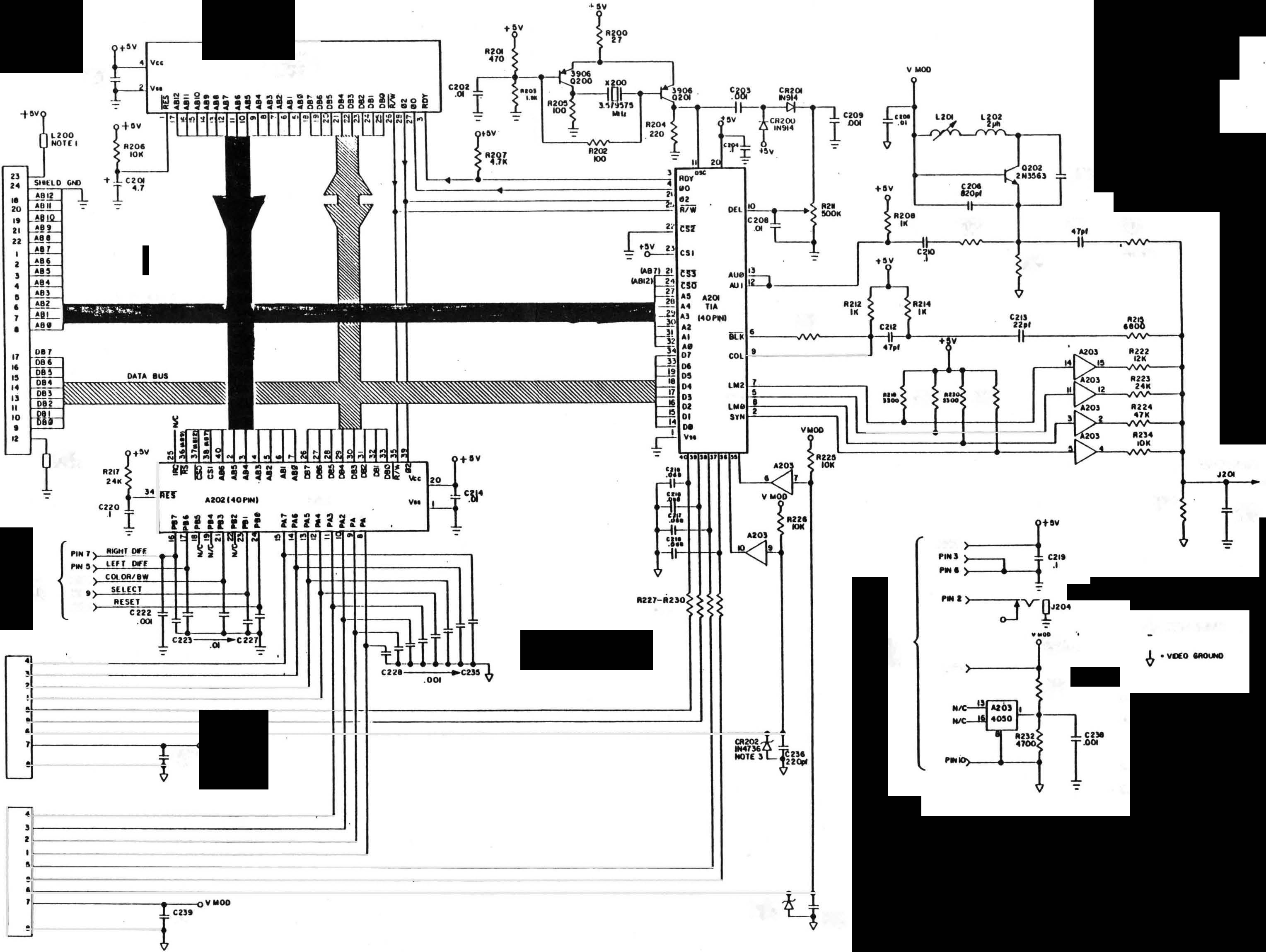
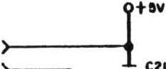
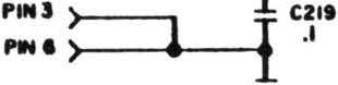
.1101 .110) ':" J201 ,fIIOW SWIfCH 10ARD LZOl HOT(t C200 .01 {""" ..... 'OI4 ,.. ,..I .tDOR£SS IUS ---------.... yMOO C240 .01 1�---------�-C�2S�.-oyWOO .01 ..00 "PU421PINI 0501 6'12 -. :.t. I.IK Rail 110 LW21�--------------_, LWI Cft20S 1H47)6 HOTES enl 220p1 JIOO ,AO.. 'wIlCH lOAIIO YMOO ... .... "ZOI II. .... .... IIIZIO .000 PI"I > ::� IC�I• CZO' ...". 021 "'II)->----r J204 .... '111•)---------i ,.,.... +$.,0"," 02)1 IlOO 0..1 ..1M IIOT[I ... .........., t---..,..--""12 02n 11K l(GlND' !.LOGICGllCUG MOTU CIII IIOff I. ,..,.1.......Of,...... .,..... UDP"'0'ha".1�"�tCN.,...... .....'...bud UOl ..,...".S"'"8ftdwcIOfM..... ......... ...... J. Me..,....."" "a.'....,aiM ........ ......... II( l IftCOfPCWM...,1,... soo,............._ ,.."1 ...... ).• 2600MotherboardSchematic
,,�5ii!:iS�'!8§§88�8��g�


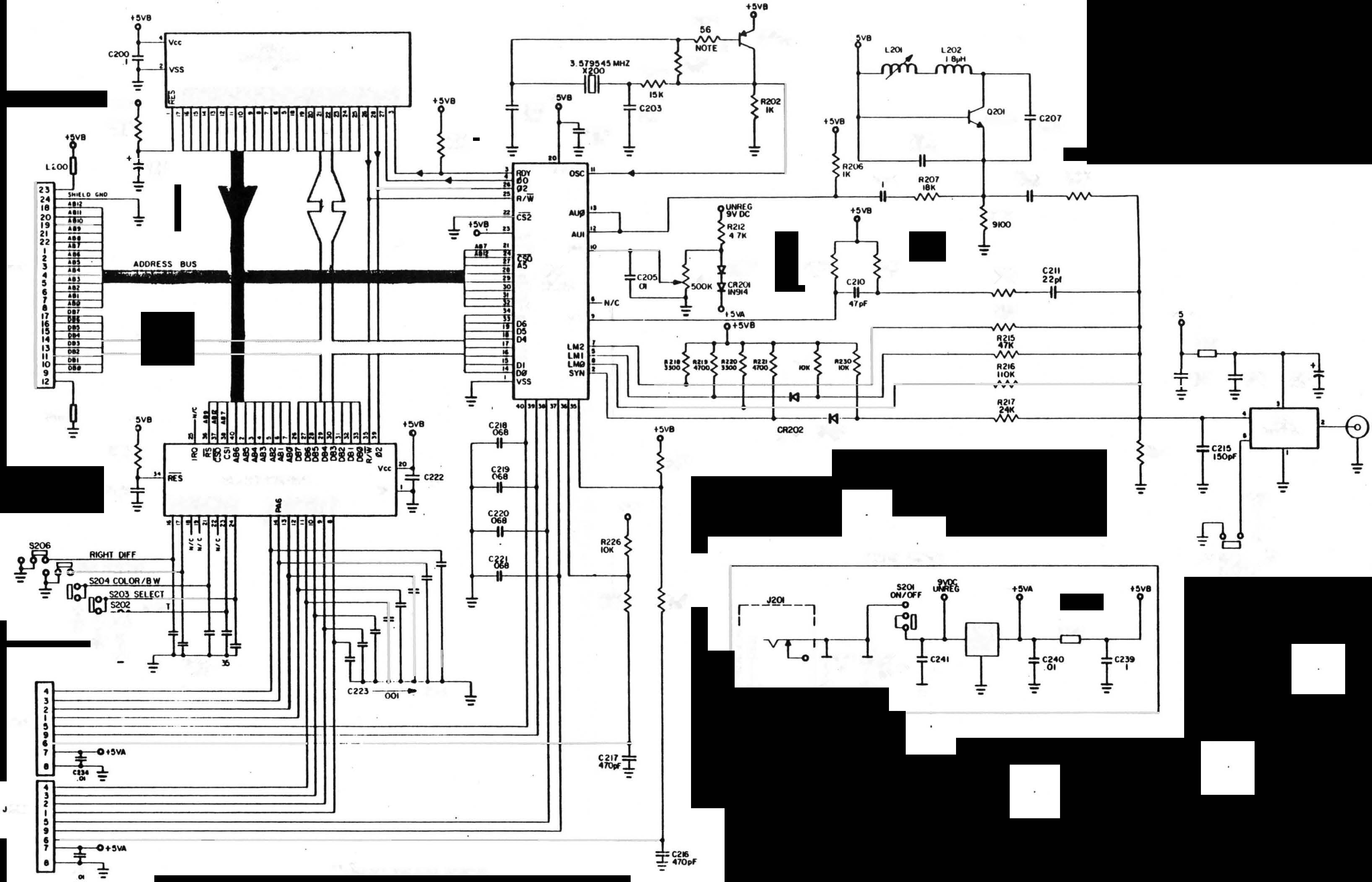

v" 4Z00 c MPUt2.PtH� 6�0' R2O!I 10k R20' �6 f..�906 • a NOTEZ AZ04 '!lOK +W8 t�
+�VB rC203 +�v8 rC202 lJIliJl RZOO III tl�8 20. L�OOI + C20t 0' NO � � �aus 0 OATA BUS JlO r-1r-ior-.�: J J L20l •�V8 = RZ21 �I Ii II!! 20. iC .202140 PIN. ''''2 -�,� \ISS '• C23e .I Hrffilff i ii'nii • • I�I' .� RIGH1'iliff S2O!I LEFT iliff '1= II: 03SELECT : J2 1 S¥o! AESE : -=lUO-l: t--: -=1 I- � * cz�-;cz .... r;- C223 e230 foz .. lO' �1� rI 20p1 C204 R20I 22 47K - ...!! Yee ...:-. �ffi�.� C$I en on ijIl t�2O!I1 A20I '0 T'A '3 '00.,," Al ., fLHIC AI 01 COL 06 � � �lnl t-- 03 02 t--I�� f, "I" C 4 .. t�v' C � .. �6: � m� 4 � 4r .-------. CH200 R21) _0 ��tOM)· � .�'" l"va t�� 2N3�1 C206 B20p1 .. .. I=C201B20p1 ;�,f' C208 _:,r-: C209 47p' ,', �L .. R208 9100 � � ftZH A22. Ul8 ,. ,. .. ���o ;�. "::: J1 .," ���. ... J�, CR202 CA2m - 1H9I� A22l 101< POWEft SUPPL' Rl2" Z20 R209 I•• r-��i o 1 1 020' L204 11 I 1'Z42 iC24' fczo, I '22oo.f , 1 1 '6V 1- 1-= -= -= L:..____.J �VIlLT IlEG cg -= R222 ,�. � j8 iczr +l..... L2O!I -tC2'2 C215 � 0' .001 �I C214 �1 t�� Rf ..OOUlE H'" J fl:: I. .:l ���NEL3 SELECT:f��pf 26001\(Revs.14and15)MotherboardSchemati � NOT[en' ± c I UNLESSOTfil.wISE SP£CIf"tEt.w �.':!.S��'Ml:�T\\Il"'�INWI 2 112m....ALSOHAVE Of390... "f OUT J200
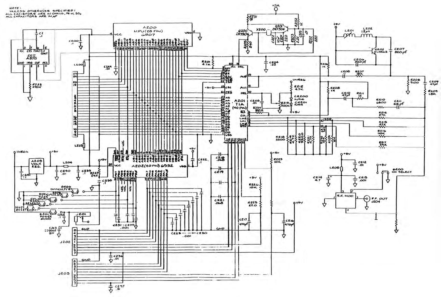
.lez.... .. J200 ,. �9 21 u , I 4 � .. 1 17 � :1 II 10 �t;;."". --11--czzo .0... I(Cz.. CtO CZli&T I�/,-f ! IU.ac I�o<.
2600A(Revs.16andup)MotherboardSchematic
