
OPTICAL BEHAVIOUR OF SYNTHESIZED ZNO
NANOTABLETS AND ITS TRANSFORMED
NANORODS WITH THE ASSISTANCE OF A
CATIONIC SURFACTANT CTAB
ABSTRACT
We are reporting the preparation of ZnOnanotabletsat relatively low temperature (1500C) using zinc acetate [Zn(Ac)2], NaOH, cetyltrimethylammonium bromide (CTAB) by solvothermal method. By adjusting the molar ratio of the reactants we obtained nanorods and we also obtained the variation of the dimension of the nanorodsusing hydrazine hydrate as capping reagent. The prepared samples were morphologically recognized as well crystallized.Theaverage diameter of the ZnOnanotabletswere ranging from 500 to 600 nm and the average thickness of the nanotabletswere ranging from 85 to 90 nm. Thelength of ZnOnanorods were ranging from 300 to several micrometersand breadth of theZnOnanorodswere ranging from 80 to 160 nm. The optical properties of the prepared materials have also been studied with the exhibition of its interesting behavior.
Keywords
Nanostructures; Thin films; Sol-gel growth; X-ray diffraction; Optical properties
1. INTRODUCTION
In recent years one dimensional (1D) semiconductor nanostructuressuch as nanorods, nanowires, nanobelts and nanotubes have been attracted great attention due to their many unique properties. The possibility of such unique properties can be exploited for obtaining as building materials of the construction of future electronics and photonics devices [1-3]. 1D semiconductor nanostructures also has their applications in life sciences[4]. They also have potential uses as interconnectors,nanoscale electronics, optoelectronics and sensing devices [5]. It is generally accepted that 1D nanostructure are useful materials for investigating the dependence of electrical and thermal transport or mechanical properties based on dimensionality and size reduction or quantum confinement effects[6].Zinc oxide having a wide direct band-gap (3.37 eV) with a large excitonic binding energy of 60 meV at room temperature, has been recently attracted due to their potential uses in ultra-violet (UV) luminescence devices, light emitting diodes (LEDs), gas sensors, solar cells and transparent thin film transistors [7]. ZnO is also a material that is biocompatible and biosafe. ZnO may be used as implantable biosensors and it also has biomedical applications.
Advanced
In the past few years, much effort has been devoted to develop various 1D semiconductor nanostructures [8-10]. Several researchers have developed various kinds of ZnO nanostructures such asnanodots, nanorods, nanowires, nanobelts, nanotubes, nanobridges and nanonails, nanowalls, nanohelixes, seamless nanorings, mesoporous single-crystal nanowires, and polyhedral cages [11-13]. Till date various synthetic methods have been reported such as vapour–liquid-solid ( VLS ) [14-16], vapour–solid (VS) [17] mechanism, laser ablation–catalytic growth [18-19], oxide–assisted growth [20], template–induced growth [21-22], solution–liquid–solid growth in organic solvents [23-24], metal–organic chemical vapour deposition (MOCVD) [25], hydrothermal synthesis, the micro–emulsion hydrothermal process, chemical vapour deposition (CVD) and a catalyst–free CVD method [26-29].They have been largely reported on the synthesis of pure ZnOnanorods/ nanowires by solvothermal/ hydrothermal methods [30-34]. Among the 1D nanostructures ZnOnanorods and nanowires have been widely studied because of their easy nanomaterials formation and device applications.
In this paper, we have preparedZnOnanotablets by the assistance of the cationic surfactant cetyltrimethylammonium bromide (CTAB). We extensively studied the variation of dimensions of ZnOnanorodsby changing the reactant’s molar ratio. We also studied that the diameter and length of the nanorods can be easily tuned by the introduction of the capping reagent hydrazine hydrate.The optical properties of the as prepared materials have been studied extensively for elaborating their comparable band gaps and photoluminescence behavior.
2. EXPERIMENTAL SECTION
All the reactants,purchased from E-Merck Germany, were of analytical grade and were used without any further purification.
a) Preparation of ZnO nanostructures
In a typical procedure to synthesize ZnO nanostructure,6.00gm of Zinc acetate (Zn(Ac)2)was put into a glass beaker filled with 15ml of double distilled water.The mixture was stirred for 10 minutes at room temperature to form a solution. Following the same procedure we make another solution putting 0.3 gm of CTAB into 10 ml of double distilled water. Then the solution of CTAB was added into the glass beaker containing the Zn(AC)2 solution and left for 15 minutes under vigorous stirring for proper mixing of the two solutions.Then we addeddropwise the as prepared 15 ml of 4M NaOH solution into the glass beaker during vigorous stirring and left for another 15 minutes under that vigorous stirring. The colour of the solution was white .Then the solution was put into a Teflon lined stainless steel autoclave.The autoclave was maintained at average 1200C for 24 hours,and then allowed to naturally cool to room temperature.The resulting white precipitate was filtered,subsequently washed with double distilled water and absolute ethanol and dried in air at 650C for 3 hours. We get nanotablets. This is the first experiment (i.e.,ZnO 1) to obtain ZnOnanotablets. To change the shape of the nanostructure we repeated the same experiment with different molar ratio of the reactants and CTAB also and we gotnanorods. Now to change the dimension of the nanorods we used hydrazine hydrateas a capping reagent in the same experiment keeping theother reactant’s molar ratio constant and at the same reaction conditions.The detailed information about other experiments is given in Table no. 1.
b) Characterization
Crystalline structureof the obtained products were characterised by X-ray diffraction studies (XRD) using a diffractometer(Bruker D8 Advance) with CuKα line.The morphology of these products was obtained by field emission scanning electron microscopy (FE-SEM) and the FESEM photos were taken with a S4800-JU at 5.0 kV.The FE-SEM measurements were done on the glass substrate coated with requisite samples using a programmable Spin Coater,Apex Instruments Co. with model No.SCU-2008C.UV-vis spectrophotometer (Model: TCC-240A,UV2401 PC,Shimadzu,Japan)was used to record the electronic absorption spectra of the obtained products at room temperature.Photoluminescence spectra were carried out on a LS55,Fluorescence spectrometer,PerkinElmer using excitation source of the 300 nm and 500 nm line of a He-Cd laser.
3. RESULTS AND DISCUSSION
a) Crystalline structure and Morphology
The structure and size of the ZnO nanostructures can easily be seen by the low and high magnification of FESEM images shown in Fig. 1 (a – h). The average thickness of the nanotablets is about 90 nm and the thickness is ranging on average from 85 to 95 nm. The average diameter of the nanotablets is ranging from 500 to 600 nm. The nanotablets are almost uniform in shape and size. The shape of the nanorods is straight.The length of the nanorods is ranging from 300 nm to several micrometers and the diameter of the nanorods is ranging from 80 to 160 nm.
different types of ZnO nanostructures. a nanotablets (ZnO 1) with 100 nm resolution, b nanotablets (ZnO 1) with 1 µm resolution, c nanorods (ZnO 2) with 100 nm resolution, d nanorods (ZnO 2) with 1 µm resolution, e nanorods (ZnO 3) with 100 nm resolution, f nanorods (ZnO 3) with 1 µm resolution, g nanorods (ZnO 4) with 100 nm resolution and h nanorods (ZnO 4) with 1 µm resolution.


The crystal structure and crystallinity of the as prepared products were investigated by XRD. Fig 2(a - d) shows a typical XRD pattern of ZnO precursors, in which all the diffraction peaks can be well indexed to the hexagonal wurtziteZnO crystal with lattice constant a =3.249 Å and c = 5.208 Å, in good agreement with the standard PDF data (JCPDS file 36–1451). No additional reflections are observed which indicates that there are no additional crystalline structures present in the samples. The strong and sharp diffraction peaks demonstrate that the products are well crystalline. The XRD patterns of ZnO samples show the characteristic hexagonal wurtziteplanes at(100), (101), (002), (102), (110), (103), (200), (112), (201), and (202)and those are located at 31.730, 34.350, 36.220, 47.520, 56.610, 62.860, 66.350, 67.890, 69.090, and 76.870 in the 2 theta range graph from 200 to 800 (Fig. 2(a-d)).In addition, the intense and sharp diffraction peaks are observed at (100), (002), (101) etc (hkl) planes. Fig 2(a – c) suggest that the obtained products are well crystallized.By using the XRD analysis, the d-spacing of the ZnOannotablets and nanorods have been calculated for the hexagonal wurtzite structures and compared with the standard JCPDS data(Table 2). In our exprriment for XRD analysis,CuKα (λ=1.5418 A) radiation is used whereas in case of JCPDS (36 – 1451), CuKα 1 (λ=1.5405981 A) radiation was used.Moreover, the Debye-Scherrer Equationis given below as:
d=0.9*λ/β cosθ .......................(1)
where ‘d’ is the breadth of the nanorods, λ= wavelength of the CuKα radiation (i.e. λ=1.5418 A), β=FWHM (Full Width Half Maxima) of the XRD peaks, θ= the angle at which the corresponding peaks occur.By using Debye- Scherrer equation (Eqn(1)) we calculated the average thickness of the nanotablets and average breadth of the nanorods. The average thickness of the ZnOnanotablets (ZnO1) is 92 nm and we get the following values of breadths of the as prepared ZnOnanorod products, those are90nm for ZnO2, 93 nm for ZnO3,and110 nm for ZnO 4.


b) Optical Properties

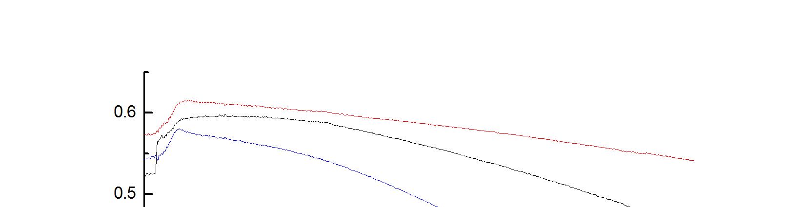
The optical properties of semiconductor nanomaterials depend on the size and shape of the particles.The UV-Vis spectra,recorded at room temperatureof the as prepared ZnO products are shown in Fig. 3. The absorption edge of ZnO products is about 500 nm and the corresponding energy is approximately 2.48 eV. The weak absorption peak is observed at 400nm and the corresponding energy is approximately 3.1eV. The excitonic absorption features are not very sharp. The optical bandgap (Eg) for semiconductors can be evaluated with the following relation as given below [35-36].

αhν =A(hν -Eg)n/hν (2)
Where, A is a constant related to the effective masses associated with the bands, n is a constant and n = ½ for a direct band gap material, 2 for an indirect band gap material and 3/2 for a forbidden direct energy gap, the estimated Eg values are in the range from 1.70 to 2.30 eV as reported earlier [19]. α is calculated with the following relation as given below [20]:
α =1/tln(1/(1-A))
(3)
We obtained the bandgap of all ZnO products by extrapolating the linear portion of the plot (αhν)2 versus (hν) as shown in Fig.4. Bandgap is changing from2.2 to 2.85 eV depending on different geometric configurations of ZnO products. The ZnOnanomaterials band gap value differs from bulk (3.37eV) material due to quantum confinement effect.
The photoluminescence spectra of the as prepared ZnOnanotablets and nanorods, recorded at room temperature for the excitation wavelength 325 nm, is shown in fig. 5. In the present work the emission property of the as preparedZnO products was studied from photoluminescence spectrum in the spectral region from 300 to 800 nm. We observed a broad peak at around 425nm and a very strong peak at around 650nm. Their corresponding energies are 2.92 and 1.91eV, respectively. Therefore the energy loss for the first peak is 0.90eV, and for the second weak peak is 1.91eV.It is clearly indicative that the difference between band gap energy and energy loss corresponding to second photoluminescence peak is ranging from 0.29 to 0.94. So that the previous difference of energy may be associated with non radiative transition. That implies that different types of excitonic energy level are formed for different types of ZnO nanostructures which is definitely associated with quantum confinement effect.


4. CONCLUSIONS
In summary, we are reporting the synthesis of ZnOnanotablets by the assistance of CTAB, a cationic surfactant. The shape of the nanotablets can be changed to nanorods by simply changing the reactant’s molar ratio. Again we have shown that the dimension of the nanorods can be changed by varying the capping reagent’s (Hydrazine hydrate) amount. The particle size and morphology was verified by powder XRD and FESEM. The optical properties are changed with the change of the size, shape and dimension of the ZnOnanoproducts. We can tune the band gap energy by simply changing the shape and size of the as prepared ZnOnanoproducts.


5. ACKNOWLEDGEMENTS
The work was supported by the funding agency DST, Government of India for providing the financial assistance with the completed project number SR/S2/CMP-0020/2009 and greatly thankful to IACS, Jadavpur for XRD and FE-SEM measurement.
REFERENCES
[1] D. Appell, Nature 419 (2002) 553.
[2] L. Samuelson, Materials Today 6 (2003) 22.
[3] X. F. Duan, Y. Huang, Y. Cui, J. F. Wang, C. M. Lieber, Nature 409 (2001) 66.
[4] Y. Cui, Q. Wei, H. Park, C. M. Lieber, Science 293 (2001) 1289.
[5] Y. N. Xia, P. D. Yang, Y. Sun, Y. Wu, B. Mayers, B. Gates, Y. Yin, F. Kim, H. Yan, Advance Materials 15 (2003) 353.
[6] K. Pal, T. Pal Majumder, S. Ghosh, S. K. Roy, Journal of Molecular Structure 1041 (2013) 16.

Advanced Nanoscience and Technology: An International Journal (ANTJ), Vol. 1, No. 1, 2015
[7] Ü Özgür, Y. I. Alivov, C. Liu, A. Teke, M. A. Reshchikov, S. DÕgan, V. Avrutin, S. J. Cho, H. Morkoc, Journal of Applied Physics 98 (2005) 041301
[8] P. D. Yang, C. M. Lieber, Science 273 (1996) 1836.
[9] A. M. Morales, C. M. Lieber, Science 279 (1998) 208.
[10] X. G. Peng, J. Wickham, A. P. Alivisatos, Journal of American Chemical Society 120 (1998) 5343.
[11] Z. L. Wang, Materials Today 7 (2004) 26.
[12] J. H. Park, H. J. Choi, Y. J. Choi, S. H. Sohn, J. G. Park, Journal of Materials Chemistry 14 (2004) 35.
[13] J. H. Park, H. J. Choi, J. G. Park, Journal of Crystal Growth 263 (2004) 237.
[14] R. S. Wagner, W. C. Ellis, Applied Physics Letters 4 (1964) 89.
[15] A. I. Klimovskaya, I. P. Ostrovskii, A. S. Ostrovskaya, Physica Status Solidi A 153 (1996) 465.
[16] O. Toshio, N. Masayuki, Journal of Crystal Growth 46 (1979) 504.
[17] Y. Iwao, S. J. Hajime, Journal of Crystal Growth 45 (1978) 511.
[18] D. P. Yu, X. S. Sun, C. S. Lee, I. Bello, S. T. Lee, H. D. Gu, K. M. Leung, G. W. Zhou, Z. F. Dong, Z. Zhang, Applied Physics Letters 72 (1998) 1966.
[19] X. F. Duan, C. M. Lieber, Journal of American Chemical Society 122 (2000) 188.
[20] R. Q. Zhang, Y. Lifshitz, S. T. Lee, Advance Materials 15 (2003) 635.
[21] W. Q. Han, S. S. Fan, Q. Q. Li, Y. D. Hu, Science 277 (1997) 1287.
[22] C. R. Wang, K. B. Tang, Q. Yang, B. Hai, G. Z. Shen, C. H. An, W. C. Yu, Y. T. Qian, Inorganic Chemical Communication 4 (2001) 339.
[23] Y. Jiang, Y. Wu, X. Mo, W. C. Yu, Y. Xie, Y. T. Qian, Inorganic Chemistry 39 (2000) 2964.
[24] C. R. Wang, K. B. Tang, Q. Yang, Y. T. Qian, Journal of Electrochemical Society 150 (2003) G163.
[25] M. Yazawa, M. Koguchi, A. Muto, M. Ozawa, K. Hiruma, Applied Physics Letters 61 (1992) 2051.
[26] C. L. Jiang, W. Q. Zhang, G. F. Zou, W. C. Yu, Y. T. Qian, Journal of Physical Chemistry B 109 (2005) 1361.
[27] X. M. Sun, X. Chen, Z. X. Deng, Y. D. Li, Materials Chemistry and Physics A 78 (2003) 99.
[28] J. J. Wu, S. C. Liu, Advance Materials 14 (2002) 215.
[29] J. J. Wu, S. C. Liu, Journal of Physical Chemistry B 106 (2002) 9546.
[30] J. Q. Xu, Y. P. Chen, J. N. Shen, Journal of Nanoscience Nanotechnology 6 (2006) 248.
[31] Y. Zhang, J. Q. Xu, Q. Xiang, H. Li, Q. Y. Pan, P. C. Xu, Journal of Physical Chemistry C 113 (2009) 3430.
[32] L. Vayssieres, Advance Materials 15 (2003) 464
[33] J. X. Wang, X. W. Sun, Y. Yang, H. Huang, Y. C. Lee, O. K. Tan, L. Vayssieres, Nanotechnology 17 (2006) 4995.
[34] L. E. Greene, M. Law, J. Goldberger, F. Kim, J. C. Johnson, Y. F. Zhang, R. J. Saykally, P. D. Yang, Angew Chemistry International 115 (2003) 3031.
[35] R. B. Kale, C. D. Lokhande, Semiconductor Science and Technology 20 (2005) 1.
[36] K. Pal, U. N. Maiti, T. Pal Majumder, P. Dash, N. C. Mishra, N. Bennis, J. M. Otón, Journal of Molecular Liquids 164 (2011) 233.