power & energy efficiency handbook


A SUPPLEMENT TO DESIGN WORLDOCTOBER 2022 Ultra-long-life lithium batteries power the IIoT Page 6 Where depletion-mode power MOSFETs excel Page 16 Calculations reveal the value of efficiency Page 19


goodbye to

used ev sales ?
there were some interesting developments at the recent and aptly named Battery Show near Detroit for those who follow battery technology. One in particular came from the Michigan-based Our Next Energy (ONE). The firm released details about a 240Ah prismatic cell battery it has designed and which is said to be the highest energy density large-format cell yet produced. Perhaps the most noteworthy fact about the new battery is that its design eliminates the need for graphite and anode manufacturing equipment—it is anode free. That lets ONE cells be produced using about half the current manufacturing equipment needed to make equivalent capacity cells today.
ONE figures it will be able to turn out the new batteries at a cost of $50/kWh. For comparison, the average new EV battery goes for around $128/ kWh, a price likely to rise because of inflation and the scarcity of rare earth minerals.
But if you buy an EV and its battery dies after the warranty expires, you’re probably going to end up paying a lot more than $128/kWh. Greencars, a website specializing in EV learning and shopping, reported in 2020 that 16 kWh Chevy Volt battery packs cost about $4,000 to replace, putting them at about $240/kWh. Keep in mind that a brand new Volt costs about $26,600 when it comes off the showroom floor. A 2011-2015 Chevy Volt remanufactured battery pack is priced at $6,000 at Greentec Auto, a company specializing in hybrid battery replacement. These batteries have 17.1 kWh of capacity, putting their price at
$350/kWh in 2021 dollars.
covers pre-owned EV transactions, points out that the cost of an out-of-warranty 100 kWh battery (as found on long-range Tesla vehicles) replaced in 2025 might range from $5,600 to $13,500, depending on whose predictions you want to believe.
These estimates assume that industry continues making advances in battery technology similar to that just announced by ONE. Today battery replacements even in budget-priced vehicles are pricey. The Nissan Leaf, which starts at about $27,800, can come with batteries ranging in size from 30 to 62 kWh. Replacement costs for these batteries range from about $3,500 to $9,500. Even hybrid EVs with their relatively smaller batteries have eye-popping battery replacement costs. Consider the 2022 Hyundai Ioniq Plug-In Hybrid which starts at $26,800. A replacement battery for a 2018 or 2019 model had an MSRP of $2,853.53 last year. The battery in the Ioniq HEV is 1.56 kWh, equating to about $1,829/kWh.
New-car warranties mean that buyers of new EVs probably don’t worry much about replacing their batteries. But EV battery cost is a top-of-mind for those of us who typically buy used cars. I myself am in this group. It was more than 30 years ago that I bought my last new car off a dealer lot. I don’t see myself buying a used EV knowing I may have to shell out 15% of what I paid for the car in a year or two when the battery gives out.


I suspect I am not the only potential used-EV buyer who thinks this way. Baring drastic improvements in EV battery pricing, the automotive industry may be faced with a new paradigm as EVs age: It may end up being impossible to sell a used EV without first replacing the battery. Alternatively, buyers like me will be unwilling to buy used EVs without a drastic price drop that far exceeds typical Blue Book depreciation for ordinary ICE vehicles today.
Whatever happens, it will be interesting to watch.
battery problems on


Most EV owners can be thankful that car makers typically warranty the battery in these vehicles for between eight and ten years and 100,000 miles. But it’s clear that out-of-warranty battery problems on EVs or hybrids can get expensive. Recurrent, an organization that

POWER & ENERGY EFFICIENCY HANDBOOK
2 DESIGN WORLD — EE NETWORK 10 • 2022 eeworldonline.com | designworldonline.com


Automotive (EVs) IT Infrastructure Wearables/HH DevicesEnterprise & Client SSD Renewables/e-Storage Power/Garden Tools AI/Video/IoT Circuit ProtectionRadar White GoodsBattery Chargers
DESIGN
FOLLOW THE WHOLE TEAM ON TWITTER @DESIGNWORLD
EDITORIAL
VP, Editorial Director Paul J. Heney pheney@wtwhmedia.com @wtwh_paulheney
Senior Contributing Editor Leslie Langnau llangnau@wtwhmedia.com @dw_3Dprinting
Executive Editor
Leland Teschler lteschler@wtwhmedia.com @dw_LeeTeschler

Senior Editor
Aimee Kalnoskas akalnoskas@wtwhmedia.com @eeworld_aimee
Editor Martin Rowe mrowe@wtwhmedia.com @measurementblue
Executive Editor Lisa Eitel leitel@wtwhmedia.com @dw_LisaEitel
Senior Editor Miles Budimir mbudimir@wtwhmedia.com @dw_Motion
Senior Editor Mary Gannon mgannon@wtwhmedia.com @dw_MaryGannon
Managing Editor Mike Santora msantora@wtwhmedia.com @dw_MikeSantora
CREATIVE SERVICES & PRINT PRODUCTION


VP, Creative Services Mark Rook mrook@wtwhmedia.com @wtwh_graphics
Senior Art Director Matthew Claney mclaney@wtwhmedia.com @wtwh_designer
Senior Graphic Designer Allison Washko awashko@wtwhmedia.com @wtwh_allison
Graphic Designer Mariel Evans mevans@wtwhmedia.com @wtwh_mariel
Director, Audience Development Bruce Sprague bsprague@wtwhmedia.com
IN-PERSON EVENTS
Events Manager Jen Osborne jkolasky@wtwhmedia.com @wtwh_Jen
Event Marketing Specialist Olivia Zemanek ozemanek@wtwhmedia.com
Event Coordinator Alexis Ferenczy aferenczy@wtwhmedia.com
MARKETING
VP, Digital Marketing Virginia Goulding vgoulding@wtwhmedia.com @wtwh_virginia
Digital Marketing Coordinator Francesca Barrett fbarrett@wtwhmedia.com @Francesca_WTWH
Digital Design Manager Samantha King sking@wtwhmedia.com
Marketing Graphic Designer Hannah Bragg hbragg@wtwhmedia.com
Webinar Manager Matt Boblett mboblett@wtwhmedia.com
Webinar Coordinator Halle Kirsh hkirsh@wtwhmedia.com
Webinar Coordinator Kim Dorsey kdorsey@wtwhmedia.com
FINANCE
Controller Brian Korsberg bkorsberg@wtwhmedia.com
Accounts Receivable Specialist Jamila Milton jmilton@wtwhmedia.com
ONLINE DEVELOPMENT & PRODUCTION

Web Development Manager B. David Miyares dmiyares@wtwhmedia.com @wtwh_WebDave
Senior Digital Media Manager Patrick Curran pcurran@wtwhmedia.com @wtwhseopatrick
Front End Developer Melissa Annand mannand@wtwhmedia.com

Software Engineer David Bozentka dbozentka@wtwhmedia.com
Digital Production Manager Reggie Hall rhall@wtwhmedia.com
Digital Production Specialist Nicole Lender nlender@wtwhmedia.com
Digital Production Specialist Elise Ondak eondak@wtwhmedia.com
Digital Production Specialist Nicole Johnson njohnson@wtwhmedia.com
VP, Strategic Initiatives Jay Hopper jhopper@wtwhmedia.com


VIDEOGRAPHY SERVICES
Video Manager Bradley Voyten bvoyten@wtwhmedia.com @bv10wtwh

Videographer Garrett McCafferty gmccafferty@wtwhmedia.com
Videographer Kara Singleton ksingleton@wtwhmedia.com
PRODUCTION SERVICES
Customer Service Manager Stephanie Hulett shulett@wtwhmedia.com
Customer Service Representative Tracy Powers tpowers@wtwhmedia.com
Customer Service Representative JoAnn Martin jmartin@wtwhmedia.com
Customer Service Representative Renee Massey-Linston renee@wtwhmedia.com
Customer Service Representative Trinidy Longgood tlonggood@wtwhmedia.com
DESIGN WORLD does
SUBSCRIPTION RATES:
SUBSCRIBER

POSTMASTER:

4 DESIGN WORLD — EE NETWORK 10 • 2022 eeworldonline.com | designworldonline.com
WORLD
2011 - 2020 2014 Winner 2014 - 2016 DESIGN WORLD does not pass judgment on subjects of controversy nor enter into dispute with or between any individuals or organizations. DESIGN WORLD is also an independent forum for the expression of opinions relevant to industry issues. Letters to the editor and by-lined articles express the views of the author and not necessarily of the publisher or the publication. Every effort is made to provide accurate information; however, publisher assumes no responsibility for accuracy of submitted advertising and editorial information. Non-commissioned articles and news releases cannot be acknowledged. Unsolicited materials cannot be returned nor will this organization assume responsibility for their care.
not endorse any products, programs or services of advertisers or editorial contributors. Copyright© 2022 by WTWH Media, LLC. No part of this publication may be reproduced in any form or by any means, electronic or mechanical, or by recording, or by any information storage or retrieval system, without written permission from the publisher.
Free and controlled circulation to qualified subscribers. Non-qualified persons may subscribe at the following rates: U.S. and possessions: 1 year: $125; 2 years: $200; 3 years: $275; Canadian and foreign, 1 year: $195; only US funds are accepted. Single copies $15 each. Subscriptions are prepaid, and check or money orders only.
SERVICES: To order a subscription or change your address, please email: designworld@omeda.com, or visit our web site at www.designworldonline.com
Send address changes to: Design World, 1111 Superior Ave., Suite 2600, Cleveland, OH 44114 WTWH Media, LLC 1111 Superior Ave., Suite 2600 Cleveland, OH 44114 Ph: 888.543.2447 FAX: 888.543.2447 2013- 2017
02 goodbye to used ev sales ?
06 ultra-long-life lithium batteries power the ii o t industrial grade lithium batteries reduce the operating costs of remote wireless sensors.

10 current sensing for energy efficient power delivery it pays to know the limitations and strengths of widely used methods of measuring current.

14 selecting a gate driver for asil-certified systems several safety features now found in gate driver integrated circuits make it easier for automotive system designs to get asil certification.

16 where depletion-mode power mosfet s excel depletion-mode mosfets have qualities that let them work well in several kinds of power-handling circuits.

19 calculations reveal the value of efficiency a few back-of-the-envelope estimates show why it pays to maximize power supply efficiency.
20 advanced capacitors enable high-efficiency energy scavenging

26 how input high-z technology keeps down adc power and size muxed sar adcs equipped with high impedance technology can substantially reduce circuit footprint and energy use without compromising performance and accuracy.
30 selecting and applying programmable power supplies a system-level view of testing is helpful when specifying power requirements.

33 interconnections for ev powertrain systems space constraints that characterize electric vehicle systems put special demands on connectors that must handle high power and rising data rates.


36 improving battery power efficiency for iot devices nanopower ship mode and sleep mode can be optimized to reduce power consumption.
40 vertical power delivery enables cutting-edge processing new architectures deliver more efficient power for today’s unprecedented high-performance

CONTENTS POWER & ENERGY EFFICIENCY HANDBOOK • OCTOBER 2022 CHECK US OUT on ISSUU.COM! CONNECT WITH US!
ultra-long-life lithium batteries power the iiot
industrial grade lithium batteries reduce the operating costs of remote wireless sensors.

at the
heart of the IIoT are lithium battery-operated remote wireless devices that bring digital connectivity to emerging and evolving technologies such as SCADA, process control, industrial robotics, asset tracking, safety systems, environmental monitoring, M2M, AI, and wireless mesh networks, to name a few.
Battery-powered remote wireless devices serve to economically capture, exchange, store, analyze, and apply data intelligently. These devices form the backbone for Industry 4.0 by eliminating the cost and complexity of hard-wiring. With numerous battery chemistries to choose from, the specifying process often revolves around five main criteria:
• Determining the energy demand
• Identifying the best battery chemistry
• Understanding the importance low self-discharge
• Adapting for high pulse requirements

• Comparing seemingly similar batteries
A remote wireless device is only as reliable as its battery, so design engineers must choose wisely based on a number of criteria, including: the amount of energy consumed in ‘active’ mode (including the size, duration, and frequency of pulses); the amount of energy consumed while in ‘standby’ mode (the base current); storage time (as normal selfdischarge during storage diminishes capacity); thermal environments (including storage and in-field operation); equipment cut-off voltage (As battery capacity is exhausted, or in extreme temperatures, voltage can drop to a point too low for the sensor to operate.), and, most critically, the annual self-discharge rate (which often exceeds the amount of energy consumed while the device operates).
Sometimes wireless devices are easily accessible for battery replacement and operate within relatively mild temperatures. Here, the approach taken could involve an inexpensive consumer-grade alkaline or lithium battery. However, an industrial grade lithium battery is typically required if the application involves a long-term deployment in a hard-toaccess location or extreme environment.
To conserve energy and extend battery life, low-power remote
6 DESIGN WORLD — EE NETWORK 10 • 2022 eeworldonline.com | designworldonline.com
POWER & ENERGY EFFICIENCY HANDBOOK
Energy Density
Power
Passivation
Elevated
at Low
Low
comparing lithium battery chemistries
for
Lithium Iron Disulfate (AA-size)
Manganese Oxide
Operating Temp.
to 85°C, can be
105°C
a short
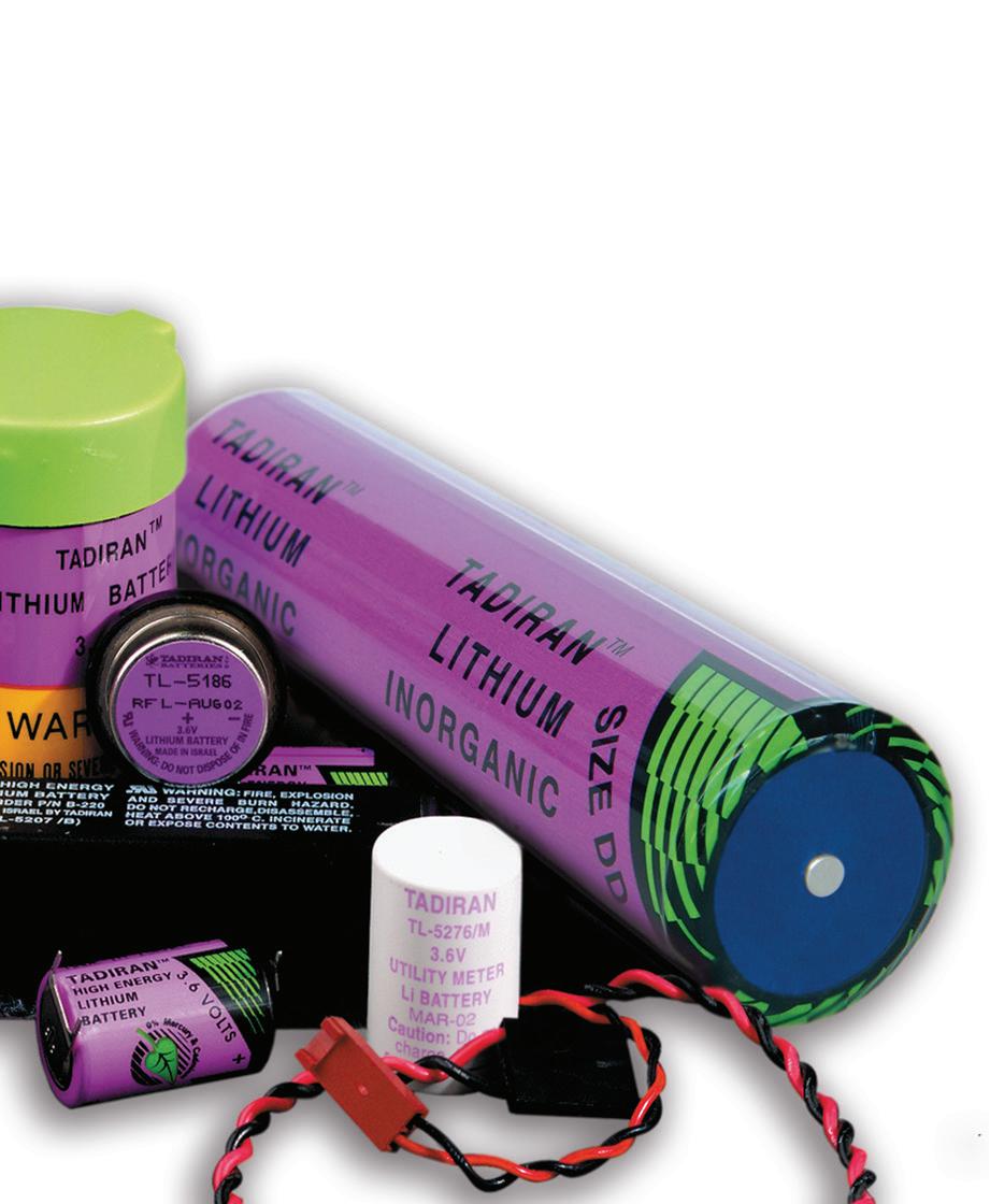
wireless devices must operate mainly in a standby state, drawing micro-amps of average current with high pulses in the multiple-ampere range. These low-power applications are predominantly candidates for bobbin-type lithium thionyl chloride (LiSOCl2) batteries, which feature a high capacity and energy density, an extended temperature range, and an exceptionally low annual self-discharge rate.
There are also certain applications that draw higher average currents measurable in milliamps with pulses that can be in the multiampere range. This kind of power dissipation can sap enough average energy to prematurely exhaust a primary (non-rechargeable) battery. As a result, these niche applications are often better suited for some form of energy harvesting device working in conjunction with
Very High Moderate
Moderate
Moderate
Moderate Poor
Excellent Excellent Moderate Fair
Very Low Very Low Moderate High
85°C -45°C
an industrial grade Lithium-ion (Li-ion) battery that stores the harvested energy.
Numerous primary (non-rechargeable) lithium battery chemistries are available, each offering their own advantages and disadvantages. At one end of the spectrum are inexpensive alkaline batteries. These cells deliver high continuous energy but suffer from a high self-discharge rate (which limits battery life), low capacity and energy density (which adds size and bulk), and an inability to operate in extreme temperatures due to water-based constituents. At the other end of the spectrum are industrial grade lithium batteries.
As the lightest non-gaseous metal, lithium features an intrinsic negative potential that exceeds all other metals, delivering the highest specific energy (energy per unit weight), highest
85°C -20°C
60°C
energy density (energy per unit volume), and higher voltage (open circuit voltage, OCV) ranging from 2.7 to 3.6 V. Lithium battery chemistries are also non-aqueous and are thus less likely to freeze in extreme cold.
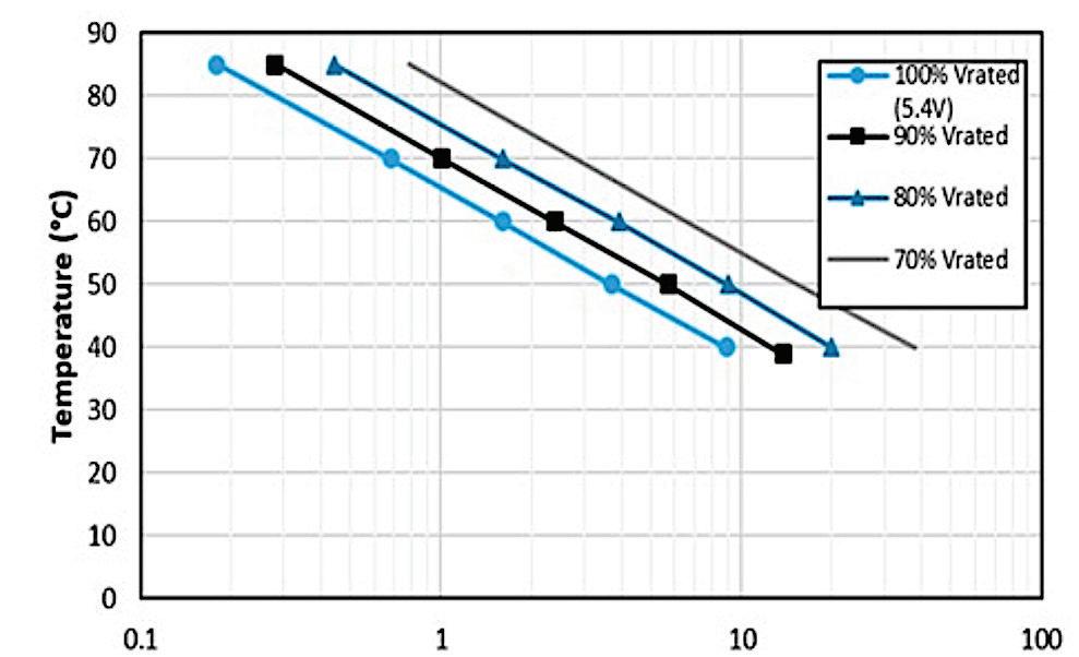
Bobbin-type LiSOCl2 chemistry is overwhelmingly preferred for long-term deployments, delivering the highest capacity and highest energy density, enduring the most extreme temperatures (-80 to +125°C), and featuring an annual self-discharge rate as low as 0.7% per year for certain cells. A self-discharge rate this low enables up to 40-year battery life. Bobbin-type LiSOCl2 batteries were specifically designed for use with low-power communication protocols such as WirelessHART, ZigBee, and LoRA. This chemistry offers the following benefits:
cattlewatch
AI-enabled electronics collars allow ranchers to remotely track their cattle herds by providing behavioral information and alerts using an ultra-low-power LoRaWAN network. Selective members of the herd carry solar-powered communicators that form a wireless mesh network covering the entire herd. Here Tadiran TLI Series rechargeable Li-ion batteries can withstand extreme temperatures, offer up to 20-year operating lives and 5,000 full recharge cycles, and can generate the high pulses required to power wireless communications.

Primary Cell LiSOCL2 Bobbin-type with Hybrid Layer Capacitor LiSOCL2 Bobbin-type Li Metal Oxide Modified for high capacity Li Metal Oxide Modified
high power LiFeS2
LiMnO2 Lithium
(Wh/Kg) 700 730 370 185 335 330
Very High Low Very High Very High High Moderate Voltage 3.6 to 3.9 V 3.6 V 4.1 V 4.1 V 1.5 V 3.0 V Pulse Amplitude Excellent Small High
Moderate
None High Very Low None Fair
Performance at
Temp. Excellent Fair Excellent Excellent
Fair Performance
Temp. Excellent Fair Moderate Excellent
Operating life Excellent Excellent
Self-Discharge Rate Very
Very Low
-55°C
extended to
for
time -80°C to 125°C -45°C to
to
to
0°C to 60°C
7DESIGN WORLD — EE NETWORK10 • 2022eeworldonline.com | designworldonline.com INDUSTRIAL LITHIUM BATTERIES
• Higher reliability – useful for remote locations where battery replacement is difficult or impossible and there’s a need for highly reliable connectivity.

• Long operating life – because the battery’s self-discharge rate often exceeds actual energy use, high initial capacity and a low annual selfdischarge rate are critical.

• The widest temperature range –bobbin-type LiSOCl2 cells can be modified to work reliably in extreme temperatures (-80 to 125°C).
• Smaller size – their higher energy density can permit the use of batteries that take up less space.
• Higher voltage – delivering 3.6 V, they could allow for the use of fewer cells.
• Lower lifetime cost – often a critical consideration because the labor and logistical expenses for replacing a battery will far exceed its cost.
low battery self-discharge
All batteries experience some amount of self-discharge as chemical reactions draw current even while the cell is not in use or is disconnected. Self-discharge can be minimized by controlling the passivation effect, where a thin film of lithium chloride (LiCl) forms on the surface of the lithium anode to separate it from the electrode. This film reduces the chemical reactions that lead to higher self-discharge. Whenever a current load is drawn from the cell, the battery experiences initial high resistance and a temporary drop in voltage until the discharge reaction begins to dissipate the passivation layer. This process repeats continually each time a load is applied.
The level of passivation can vary based on numerous variables, including the cell current discharge capacity, the length of storage, storage temperature, discharge temperature, and prior discharge conditions, as partially discharging a cell and then removing the load increases the level of passivation over time. Passivation may be helpful for reducing self-discharge, but too much of it can be problematic if it overly restricts energy flow.
Bobbin-type LiSOCl2 cells range considerably in terms of their ability to harness the passivation effect. For example, the highest quality LiSOCl2 cells can exhibit a self-discharge rate as low as 0.7% per year, thus retaining nearly 70% of their original capacity after 40 years. Conversely, lower-quality LiSOCl2 cells can have a self-discharge rate as high as 3% per year, exhausting nearly 30% of their
available capacity every 10 years.
To support two-way wireless communications, numerous low-power devices require periodic high pulses of up to 15 A. Standard bobbin-type LiSOCl2 cells can’t deliver high pulses because of their low-rate design. The solution is the addition of a patented hybrid layer capacitor (HLC). With this hybrid approach the standard bobbin-type LiSOCl2 cell delivers nominal background current during ‘standby’ mode while the HLC delivers high pulses to power data communications. The HLC also experiences a unique end-of-life voltage plateau that can be interpreted to generate ‘low battery’ status alerts.
Supercapacitors sometimes serve as power sources for consumer products, but they are poorly adapted to industrial applications. They have serious limitations that include short-duration power; linear discharge qualities that do not allow for the use of all available energy; low capacity; low energy density; and self-discharge rates up to 60% per year.
Supercapacitors linked in series also require the use of expensive cell-balancing circuits that add bulk and drain additional current that can further shorten their operating life.
With any long-term deployment it can be useful to have the battery last for the entire lifetime of the device, thus eliminating the need for battery change-outs. Unfortunately, it can be extremely difficult to distinguish a higher-quality cell from a poorer quality competitor because cell capacity losses caused by self-discharge may not reveal themselves for years. Additionally, the theoretical models and algorithms used to calculate battery life expectancy tend to be highly unreliable; they often underestimate the passivation effect as well as long-term exposure to extreme temperatures.
These uncertainties force designers to perform careful due diligence when evaluating batteries for any long-term deployment. As part of the specifying process, competing battery suppliers should be required to provide fully documented and verifiable test results as well as actual in-field performance data under similar loads and environmental conditions.
Learning to recognize the subtle differences between seemingly identical batteries with thorough due diligence will pay long-term dividends by increasing product longevity to achieve a lower cost of ownership.
references tadiran batteries, www.tadiranbat.com
POWER & ENERGY EFFICIENCY HANDBOOK
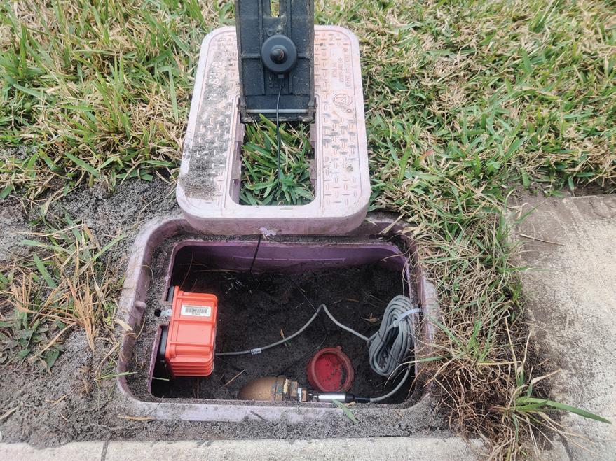
ayyeka
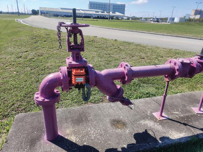
AI-enabled smart sensors are used to monitor and better maintain hard infrastructure used in solid waste and wastewater management, public utilities, transportation, energy exploration and distribution, smart cities, environmental monitoring, and more. Powered by Tadiran bobbin-type LiSOCl2 batteries, these remote wireless devices permit two-way communications to maximize operational efficiency, detect unusual events, enable predictive maintenance and repairs, and help counter cyber security threats.
8 DESIGN WORLD — EE NETWORK 10 • 2022 eeworldonline.com | designworldonline.com


 KYOCERA AVX is a leading global manufacturer of advanced electronic components engineered to accelerate technological innovation and build a better future.
current sensing for energy efficient power delivery
recent technological developments such as fast dc charging for electric vehicles or high-power processing in data centers drive the quest for delivering more power in smaller spaces. Congruent with that quest is the need for high efficiency to minimize wasted power.
AC/DC power supplies, switching dc/ dc converters, and dc/ac inverters that implement power factor correction are all power conversion systems that use current feedback to regulate properly and efficiently. Thus designers of such systems must understand current sensing and how it plays into overall system design and performance. There are various current
sensing methods in power delivery, all with their own advantages.
Some power conversion controllers have integrated current sensing, usually via an on-board amplifier connected to an external shunt. While this approach is relatively simple, many integrated solutions are optimized for a specific application and don’t adapt well to others. Consequently, many topologies instead use a generic microcontroller and external current sensing to send information back to the controller. Besides the traditional current sense amplifier and shunt, approaches to current sensing typically seen in power conversion systems include the use of an isolated amplifier and shunt, and Hall-effect current sensors.
Traditional shunt approaches can be
10 DESIGN WORLD — EE NETWORK 10 • 2022 eeworldonline.com | designworldonline.com POWER & ENERGY EFFICIENCY HANDBOOK
it pays to know the limitations and strengths of widely used methods of measuring current.
sam
locke • allegro microsystems
economical, but demands for high accuracy can boost the cost of the shunt. Shunts also offer superior accuracy at low currents (<2 A) compared to magnetic sensing.
Current-sense amplifiers are often limited by their commonmode voltage range. Commonmode voltage is the average voltage between the inputs of the current-sense amplifier and usually ranges from -10 V up to +100 V. Traditional amplifiers cannot handle the negative voltage of an ac source. The +100 V maximum also limits the use of traditional amplifiers in high-voltage dc applications unless the sensor
is close to ground. But a sensor with one terminal close to ground eliminates the ability to detect a short and creates a voltage drop from system ground and actual ground. Use of isolated amplifiers removes the limitation of sensing negative and high positive voltages but at the expense of reduced bandwidth, the need for an isolated supply, more PCB space, and higher cost.
One drawback to any shunt approach is the dependence on shunt parameters such as tolerance, temperature drift, and parasitic inductance. All these factors affect overall system
accuracy and performance. At high switching speeds common in power conversion, shunt inductance boosts the overall shunt impedance. As frequency rises, so does the shunt impedance which will reduce the overall system accuracy and speed as well as cause output spikes.
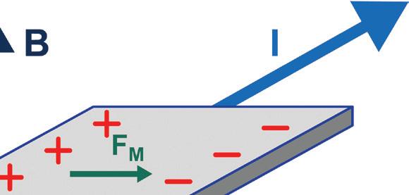
Hall-effect current sensing measures the voltage (VHALL) across a biased Hall plate created by the magnetic field (B) of a current-carrying (I) wire. Hall-based approaches have the benefit of inherent galvanic isolation and working voltages up to >1,000 V. This property lets them find

use in ac and dc high-voltage applications without the need for a secondary isolated supply.


Internal conductor Hall sensors are highly integrated and require no external shunt, facilitating their use in tight layout designs. Additionally, because sensing takes place magnetically, the conductor inductance doesn’t affect the sensor output, especially helpful for mitigating output spikes when the current switches on and off. Another benefit is that the internal conductor has a low resistance. This low resistance gives the Hall-based approaches power losses lower than those of
totem-pole pfc circuit
CURRENT SENSING
the basic principle of the active power factor correction is to force the input current waveform to track the input voltage waveform so that the sinusoidal of the ac input current synchronizes with the ac input voltage.
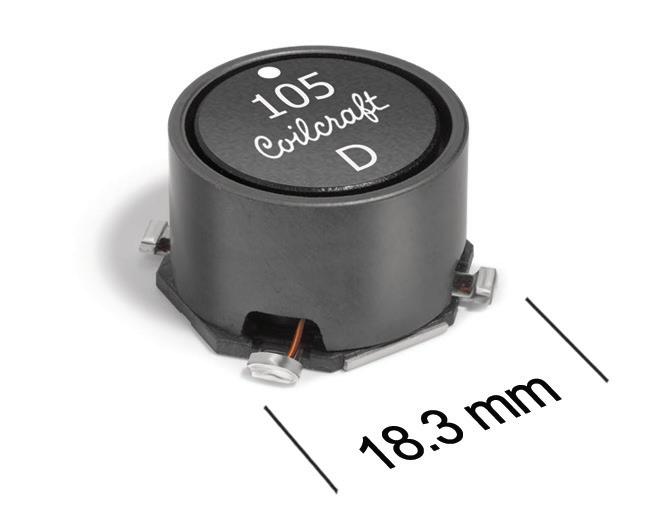
widely used current-sensing approaches compared Current sense amplifier Hall-effect current sensor Sensing method Shunt Hall effect Positive working voltage <100 V Up to >1000 V Accuracy Medium-high Medium Negative working voltage Typically -5 to 10 V Down to ≤1000 V Level of integration Low High PCB footprint Medium Small Immunity to switching noise Medium-low High Power loss Medium-high Low Cost Low-medium Medium comparison of current sensing solutions MSS1812T Series High Temperature Shielded Power Inductors • Seven inductance values from 100 to 1000 µH • Excellent current handling with low DCR • Low-loss ferrite drum core for flat inductance vs. current • Cost-effective option for a variety of applications Full Specs & Free Samples @ coilcraft.com
the hall effect principle of operation


bandwidth is typically two to ten times faster than the switching speed to allow for adequate feedback. This requirement implies a 100 kHz to 1 MHz current sensor bandwidth. Isolated current-sense amplifier circuits are typically limited to 300 kHz while Hall solutions can reach up to 1 MHz.
Electronic circuits run on a wide range of dc voltages, hence the need for dc-to-dc conversion either on the ac/dc output or for systems with multiple dc rails. DC/ DC topologies include but are not limited to the buck, boost, buckboost, flyback, and resonant.
have relatively low switching speeds (often a few kilohertz to a few megahertz) and consequently require less bandwidth.
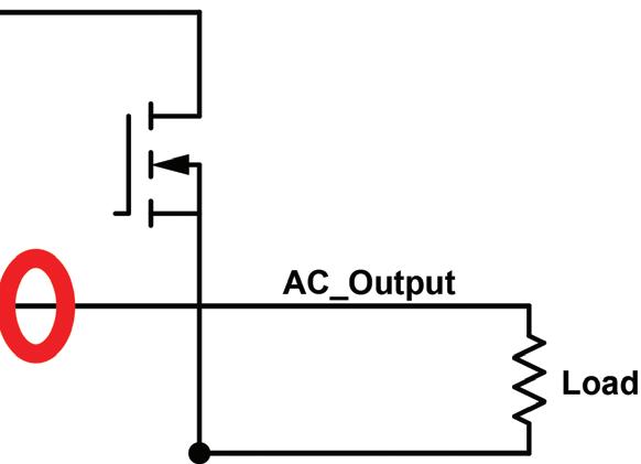
Non-isolated current sensing, such as traditional current-sense amplifi ers with shunts, can work in inverters, but the sensor must sit next to ground instead of in-phase with the ac output. This confi guration limits the ability to detect output shorts and creates a voltage drop from system ground and actual ground. This low-side sensor placement can only sense current when the low-side switch is on.
the hall effect: a magnetic field is applied at right angles to the current flow in a thin film, generating an electric field which is mutually perpendicular to the current and the magnetic field and which is directly proportional to the product of the current density and the magnetic induction.

shunt-based approaches and an advantage at higher current levels.
power factor correction Power factor correction (PFC) applied to ac-to-dc conversion aims to reduce the reactive power required from the utility and improve overall efficiency. In ac systems, inductive loads such as motors, coils, or transformers can cause the current to become out of phase with the voltage. This creates reactive power that is generated but does no actual work. Reducing reactive power boosts overall system efficiency.
There are many PFC topologies including passive
filtering techniques, boost PFC, dual boost bridgeless PFC, and totem-pole bridgeless PFC. As efficiency requirements rise, so too does complexity and cost. Totempole topologies are becoming widely used because of their high efficiency, in some cases reaching above 99%.
All active PFC topologies require sensing of the input current and voltage to regulate output and reduce phase separation. The high line voltage requires an isolated approach such as the Hall-based or an isolated amplifier. Switching speeds of PFC circuits are kept high to reduce power loss, typically from 50 to 100 kHz. Current sensor
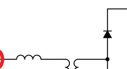
resonant dc-dc converter circuit
A resonant topology has the advantage of compact size, high power density, and galvanic

In-phase isolated amplifiers or Hall-based approaches eliminate the ground difference, enable
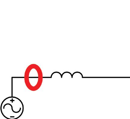
single-phase inverter circuit
a resonant dc-dc converter circuit. red circles show current sensing locations. the sensor on the left is for the input current and requires isolation. current sensors on the right are for output current located either on the low or high side depending on the selected approach.
a single-phase inverter circuit. red circles show current sensing locations. one circle represents in-phase sensing, before the load, while the other represents low-side sensing where the sensor sits between the load and ground.
isolation. These qualities earn it wide use in EV charging and energy storage. Hall-based current sensing is particularly advantageous in high-voltage dc topologies with high-isolation requirements (>100 V). Switching frequencies and bandwidth requirements for dc/dc resemble those of PFC topologies, 100 kHz to 1 MHz.
Inverters take a dc voltage and transform it into an ac voltage. Inverters fined use when dc sources such as solar arrays or batteries feed power into the grid or for powering large ac motors. Inverters typically
short detection, and can sense current regardless of switching state. This same concept can be applied to current sensor placement in motor control.
reference allegro microsystems, www.allegromicro.com
12 DESIGN WORLD — EE NETWORK 10 • 2022 eeworldonline.com | designworldonline.com POWER & ENERGY EFFICIENCY HANDBOOK


VISIT OUR EXCITING NEW WEBSITE: www.picoelectronics.com Transformers & Inductors, DC-DC Converters, AC-DC Power Supplies The big name in miniature components.The big name in miniature components. DC-DC CONVERTERS 2V to 10,000 VDC Outputs — 1-300 Watt Modules TRANSFORMERS & INDUCTORS Think Pico SmallOver 5000 std Ultra Miniature • MIL/COTS/Industrial Models • Regulated/Isolated/Adjustable Programmable Standard Models • New High Input Voltages to 900VDC • AS9100D Facility/US Manufactured • Military Upgrades and Custom Modules Available Surface Mount & Thru Hole Military • COTS • Industrial• Ultra Miniature Designs • MIL-PRF 27/MIL-PRF 21038 • DSCC Approved Manufacturing • Audio/Pulse/Power/EMI Multiplex Models Available • For Critical Applications, Pico Continues to Be the Industry Standard .18" think... ht. The most demanding applications require the world’s most reliable components. For over 50 years PICO Electronics has been providing innovative COTS and custom solutions for Military, Commercial, Aerospace and Industrial applications. Our innovative miniature and sub-miniature components are unsurpassed in any industry. PICO Electronics’ products are proudly manufactured in the USA and are AS9100D Certified. To learn more about our products and how you can benefit from our expertise visit our website at picoelectronics.com or call us today at 800-431-1064. low profilefrom Call Toll Free: 800-431-1064 E Mail: Info@picoelectronics.com • FAX: 914-738-8225 143 Sparks Ave, Pelham, NY 10803 PICO Electronics Inc.
selecting a gate driver for asil-certified systems
several safety features now found in gate driver integrated circuits make it easier for automotive system designs to get asil certification.
david divins • infineon technologies
the
Automotive Safety Integrity Level (ASIL) is a risk classification system defined by the ISO 26262 standard for the functional safety of road vehicles. There are four ASIL safety levels identified by ISO 26262—A, B, C, and D. ASIL A is the lowest level while ASIL D represents the highest level of automotive hazard. Systems like airbags, anti-lock brakes, and power steering must have an ASIL-D grade because the risks associated with their failure are greatest. Less critical systems are specified for lower levels.
ASIL certification is awarded at the system (or subsystem) level and not at the component level. But the number and type of safety features included in a component can help simplify the certification process for equipment manufacturers.
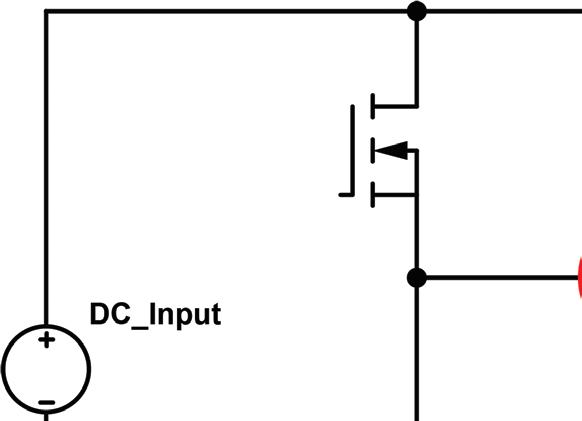
A typical application for a gate-driver IC is in the power switching of an electric vehicle’s traction motor. These switching devices are typically either insulated gate bipolar transistors (IGBT) or silicon carbide (SiC) transistors. Functions of the gate driver in this application include:
Amplification: The gate driver amplifies the low-voltage control signals from a microcontroller (MCU) to the higher voltage levels necessary to drive the power switching devices.
Isolation: A gate driver protects the low-voltage MCU from the much higher (and potentially damaging) voltages on the switching side.
Safety: In addition to protecting the MCU, a gate driver IC must include safety features to protect the overall system and hence its users. In an automobile these are the driver and vehicle passengers.
When it is part of an ASIL-compliant automotive system, a gate driver must accomplish three key objectives. First, it must
be able to continuously self-monitor (to ensure it is operating correctly) and provide feedback in the event of failure. Apart from power-up monitoring, other desirable features include testing for communications across the isolation barrier, running a register memory test (e.g., parity check), doing an oscillator frequency check, measuring internal chip temperature, and implement a life sign watch dog function.
Second, the gate driver must continuously monitor the switching of the power semiconductor device. This action requires a combination of dynamic gate-voltage monitoring (during voltage transitions) and static gate-voltage sensing (at steady state). Power supply monitoring should include checks on all primary and secondary power supply rails including under- and overvoltage detection and also a test for a zero-volt connection reference for both the primary and secondary side (to ensure return paths are intact). Finally, the gate driver must continuously monitor and protect the semiconductor switching device itself. These actions can take place using the following safety checks.
14 DESIGN WORLD — EE NETWORK 10 • 2022 eeworldonline.com | designworldonline.com POWER & ENERGY EFFICIENCY HANDBOOK
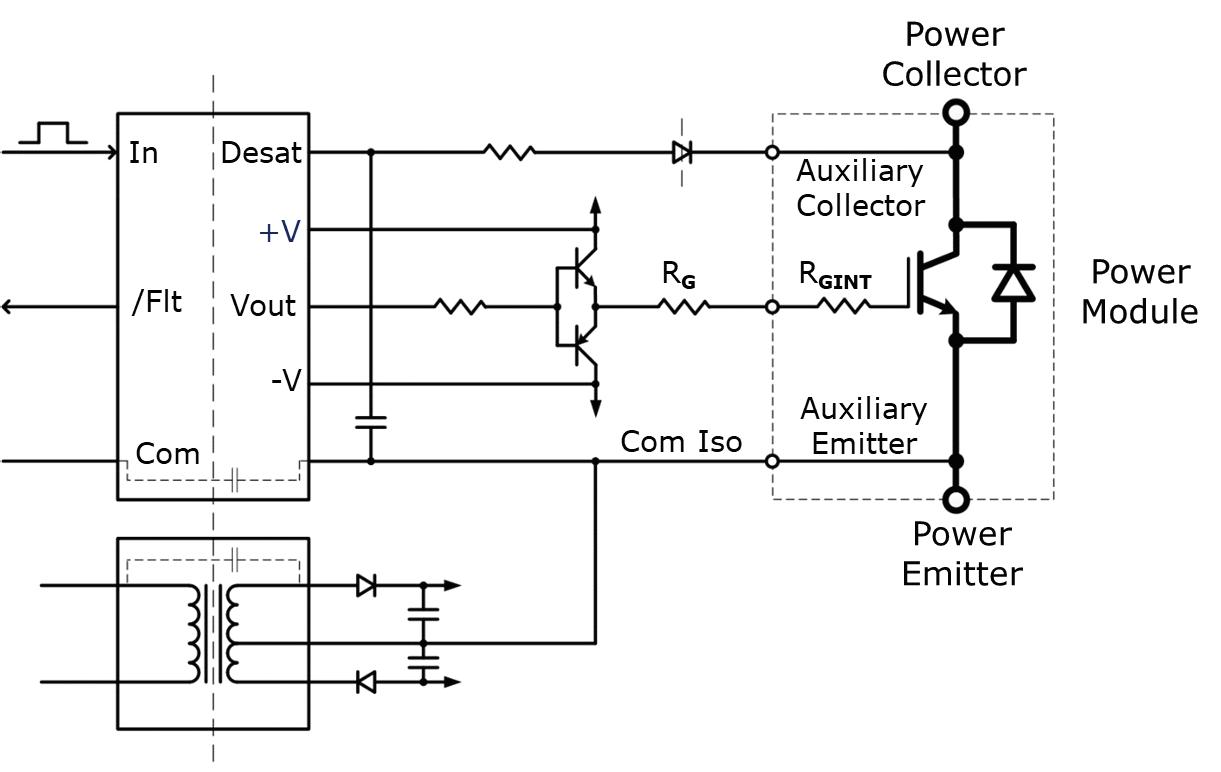
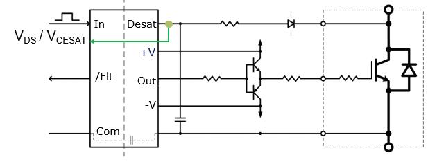
a typical gate driver application circuit. Primary power supply Primary side Secondary side Secondary power supply Output state monitoring Output stage Miller clamping Current sense Desat sense circuit Temperature sense Internal temperature sensing Active clamp control 2 level turn off ADC Shoot through protection Switching protection Serial communications e.g. SPI Secondary status Reset ADC read-out Error notification Isolation barrier Internal supervision device level (green) and board level (blue) safety features.
EFFICIENT
temperature, voltage and current monitoring
The gate driver can be used to measure the temperature, voltage and/or current of the switching semiconductor. This information can then go to the MCU to determine if measured values are within the correct operating range. When driving a discrete device,
desaturation detection ( desat ) .
the temperature of the switching device directly from the internal temperature monitor while also watching the voltage levels the dc bus.
Desaturation detection (Desat) is a useful feature for monitoring the VDS of a SiC MOSFET or the
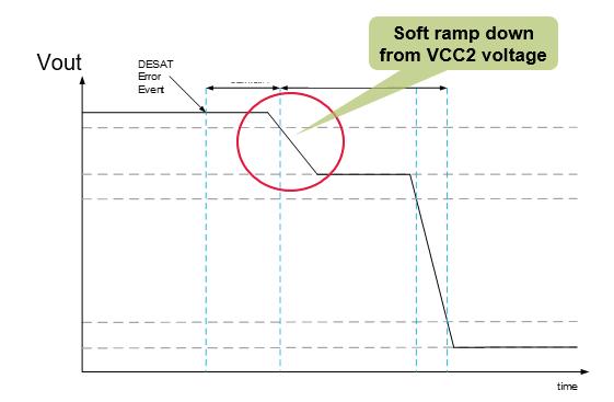
During a desat event, the combination of short-circuit current and parasitic board inductance can cause a large overvoltage. This effect can be mitigated by using two-level turn-off to slow device switching action. This turn-off technique involves briefly putting the gate at an intermediate voltage before full turn-off, thus reducing the rate at which the short-circuit current drives the parasitic board inductance, thereby lowering the overvoltage.
The presence of noise in some environments can make Desat less effective. For example, capacitive loading on long motor cables can couple noise onto the Desat pin of the gate driver, causing false trips. False tripping can be mitigated by holding the Desat sense pin of the gate driver low for a short time interval (blanking time) until noise transients have died out. For longer-duration transients, additional filtering may be necessary.
shoot-through protection Shoot-through arises when both the high- and low-side devices in a half-bridge conduct simultaneously, leading to a short-circuit. To prevent this short-circuiting, a certain amount of “dead-time” (where both devices are off) should be programmed into the MCU.
While the use of monitoring and safety features in a gate driver IC can help reduce the chance of problems and mitigate their effects, these practices should never be used as substitutes for industry-standard double-pulse and corner (voltage, current and temperature) testing. Design engineers must decide which features their specific application demands. Challenges which designers must overcome include complex error handling, setup, and optimization of programmable features (many of which are power semiconductorspecific) and programming.
two-level turn-off of a switching device to reduce overvoltage.
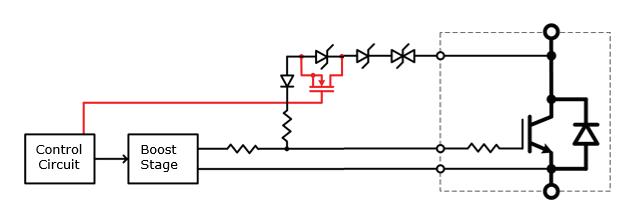
A Zener stack in series with a regular diode can be used to perform a clamping function in the event of a fast overvoltage. To further improve the noise margin, the clamping voltage can be modified to include an additional MOSFET whose gate connects to the control circuit.
Testing of power semiconductor performance under the full range of normal and fault operating conditions is always recommended.
reference infineon technologies, www.infineon.com
a mirror of the emitter current can be used to drive a negative temperature coefficient thermistor (NTC) or a temperature-sensing diode. The generated voltage can then be used to create a digital representation of the device temperature. If driving a module, a gate driver can be used to read
VCESAT of an IGBT. However, for Desat to be effective, an IGBT must have a short circuit rating. Some SiC MOSFETs also specify a short-circuit rating, but Desat is not recommended in applications which use standard silicon MOSFETs because they switch too quickly for it to work.
use of a zener stack to improve active clamping.
The Miller capacitance at the gate of the switching device can cause ringing, resulting in the unwanted parasitic turn-on of the upper switching device in a halfbridge circuit. This turn-on can lead to EMI and heating problems and potentially even cause device failure. A Miller clamp at the output of a gate driver IC can prevent this problem. A Miller clamp lowers the output impedance of the gate driver if the parasitic ringing exceeds a certain level (detected using a sense node at the switch output). The lower output impedance reduces the amplitude of the ringing and makes a parasitic turnon less probable.
15DESIGN WORLD — EE NETWORK10 • 2022eeworldonline.com | designworldonline.com
GATE DRIVING
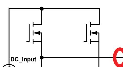
where depletion-mode
power mosfets excel
depletion-mode mosfets have qualities that let them work well in several kinds of power-handling circuits.
aalok bhatt, josé padilla, raymon zhou • littelfuse, inc.
output characteristic: enhancement mosfet output characteristic: depletion mosfet
the significant differences between the mosfets in their output characteristics.
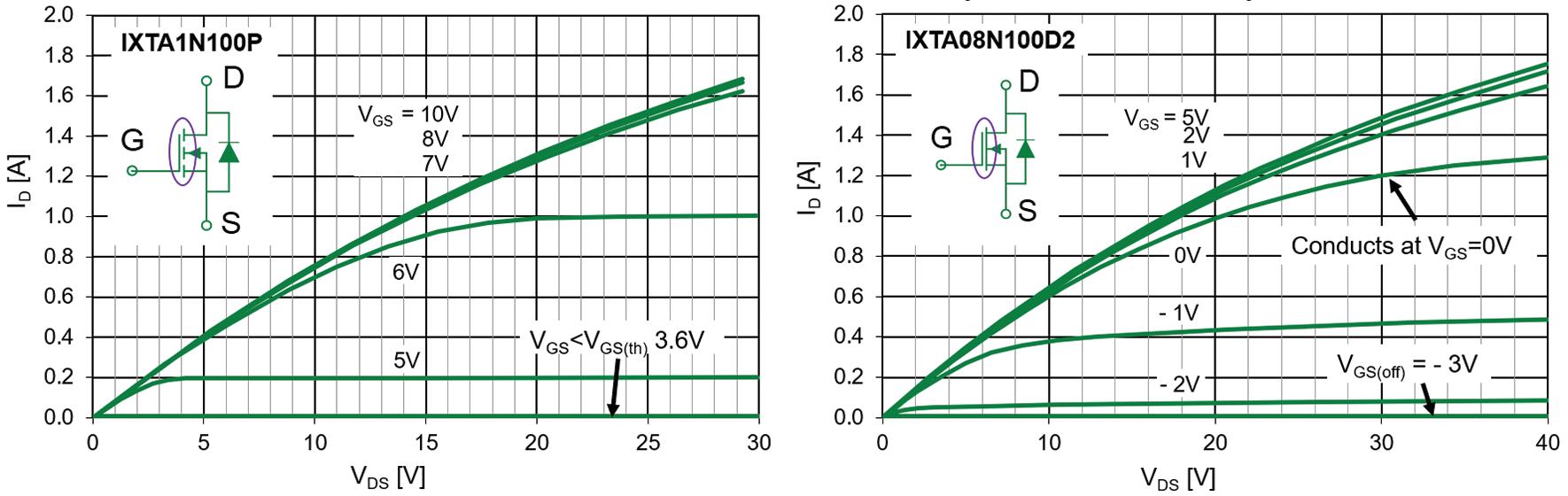
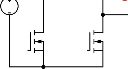
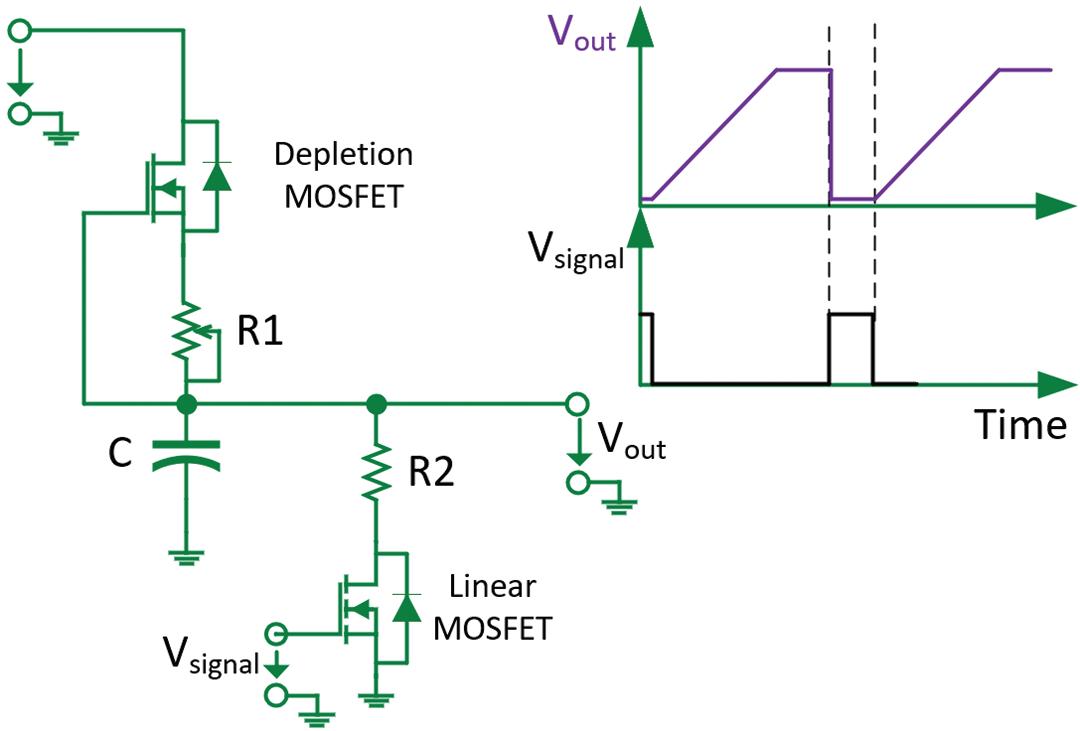
most MOSFETs are enhancementmode (EM) devices: When their gate-source voltage is zero, they don’t conduct. When the need is for a switch that is normally on when there is no power applied, depletion-mode (DM) MOSFETs fit the bill: When their Vgs = 0 V, they conduct. Unlike EM devices, DM devices don’t find use in high-speed switching. Nevertheless, there are numerous applications where DM devices come in handy. It is worth examining the properties of these less well-known MOSFETs.
As mentioned, EM MOSFETs have no conduction at Vgs = 0 V. Conduction starts at gate-to-source threshold voltage VGS(th). For the EM device, the drain current ID rises when Vgs >VGS(th). The EM device ceases to conduct at Vgs <VGS(th). In contrast, current in the DM device rises when Vgs >0. A negative gate voltage Vgs reduces the current ID, and the device stops conducting at gate-to-source cut-off voltage VGS(off)
The fact that an EM device doesn’t conduct at Vgs = 0 V means it cannot directly replace a DM device. An additional point to note is that some DM applications need no gate-drive circuit because the gate gets biasing from the circuit in which it is implemented. Thus the use
of DM devices can reduce complexity and costs while improving reliability thanks to the ability of DM MOSFETs to operate in linear mode. Usually, EM devices are incapable of linear mode operation, except for linear MOSFETs. (As a quick review, MOSFETs operating in the linear region have an ID governed only by VGS and which remains constant for any given VDS In other words, the MOSFET behaves like a constant-current sink. In this operating mode, MOSFETs typically dissipate higher power than when they are switching because of
simultaneous high voltage and current. Ordinary EM MOSFETs designed for switching may not last long if they operate in the linear region.)
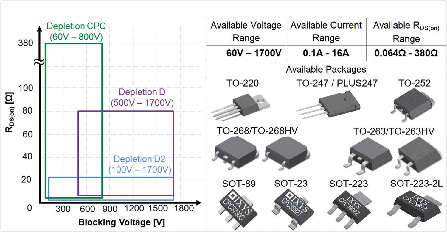
The Littelfuse depletion-mode power MOSFETs include a vertical double-diffused MOSFET (DMOSFET) structure. All these devices can sustain linear mode operation thanks to their extended Forward Bias Safe Operating Area (FBSOA). Littelfuse depletion-mode MOSFETs are known as Depletion D, Depletion D2, and Depletion CPC product families.
littelfuse depletion-mode mosfets d, d 2 and cpc family
depletion-mode littelfuse product portfolio overview.
POWER & ENERGY EFFICIENCY HANDBOOK 16 DESIGN WORLD — EE NETWORK 10 • 2022 eeworldonline.com | designworldonline.com
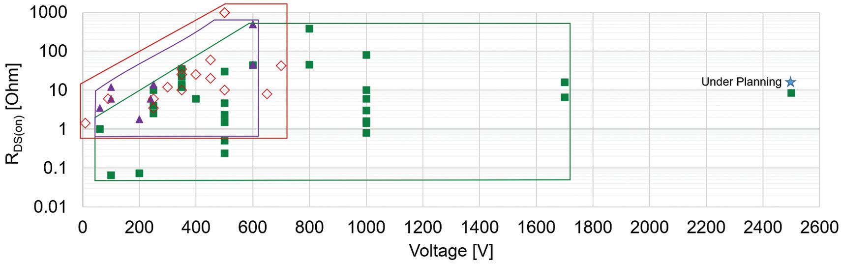
market make-up of dm mosfet suppliers
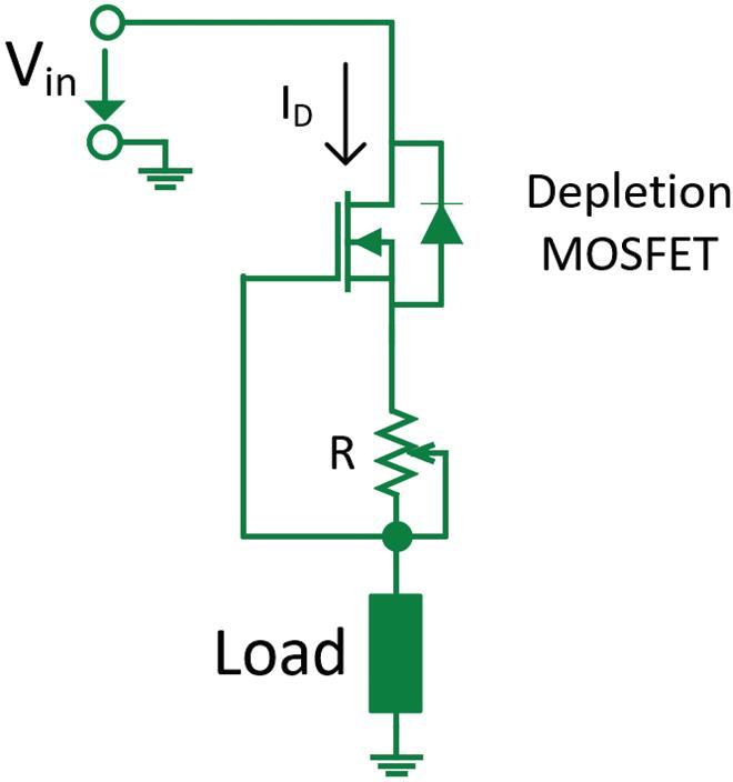
depending on the value of a resistor in series with the load and the gate cut-off voltage VGS(off). The drain current is thus independent of the input voltage. Current source circuits can be found in LED array drivers, trickle charger circuits maintaining battery charge, or to charge capacitors at a constant rate.
High-voltage DM MOSFETs with 2,500-V ratings are currently under development. Typical applications for these devices are in high voltage (HV) test equipment, power supply, ramp generator, insulation resistance test equipment, and auxiliary power supplies for HV power transmission systems.
applications of dm mosfets
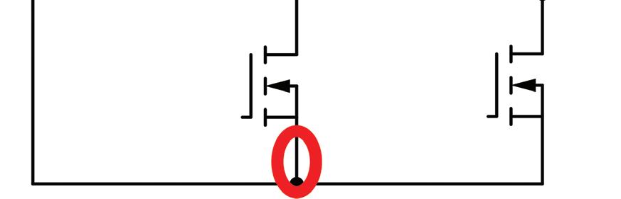
It may be useful to examine a few applications that are particularly suited to DM MOSFETs. First consider the start-up circuit of a switched mode power supply (SMPS). Here the conventional start-up circuit uses a power resistor and a Zener diode sitting in parallel with the load. In this approach, the power resistor continuously consumes power after the start-up phase. The result is excessive heat on the printed circuit board (PCB), poor efficiency, and an SMPS with limited input voltage operating range.
Alternatively, a DM MOSFET can provide the initial current required by the PWM IC to kickstart the operation. After the startup phase, the auxiliary winding
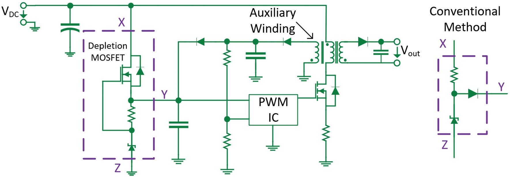
will generate the necessary power for the PWM IC. During normal operation, the depletion MOSFET draws minimal power because of its low quiescent current.
significant voltage variations, including high-voltage spikes due to the application environment.
Here the DM MOSFET is typically connected in a source
Another DM constant-current application to consider is the high-voltage ramp generator which basically constructs a ramp voltage via an RC circuit. Automatic test equipment, as an example, require high-voltage ramps with a linear relationship between output voltage and time. The constant
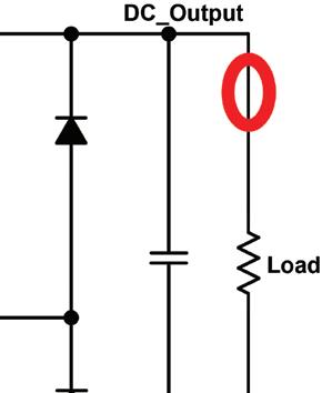
a surge-protection circuit employing a dm mosfet.
The main advantage of this approach is theoretically zero power dissipation after the start-up sequence thus improving overall efficiency. Moreover, the resulting circuit takes up a smaller area on the PCB. It also handles a wide range of dc input voltages, essential for many applications such as solar inverters.
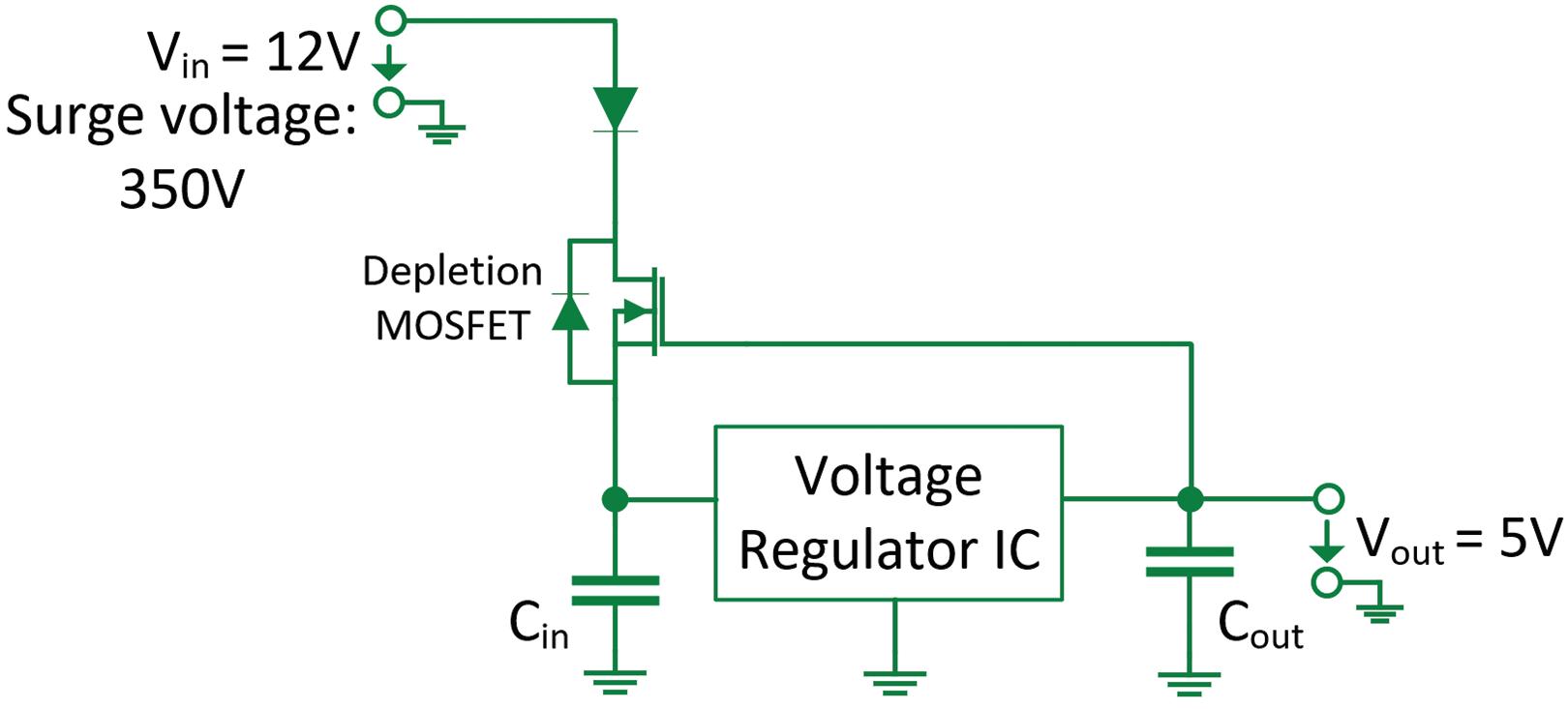
Another DM application to consider is surge protection for linear voltage regulators. Linear voltage regulators power small analog circuits, CMOS ICs, and other loads requiring low current where the input voltage Vin comes directly from a bus voltage. This power arrangement might have
follower configuration: The voltage on the source follows the voltage on the gate. The DM MOSFET conduction depends solely on its gate voltage and is independent of its drain voltage. This configuration will mitigate any voltage transient up to the withstand capability of the device voltage rating VDS
The advantage of a DM MOSFET here is it makes possible a wide dc operation voltage range Vin and minimal power dissipation thanks to the low MOSFET quiescent current. Such protection comes in handy for mitigating transients caused by lightning strikes in telecommunication circuits. A similar use is in automotive and aviation electronics to mitigate transients caused by inductive loads.
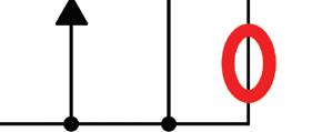
Additionally, DM MOSFETs can be the basis of constant current sources. This circuit supplies a constant current to the load
dm mosfet in smps start-up circuit.
current source charges a capacitor via a resistor and generates a voltage ramp across the capacitor. A linear MOSFET connected in parallel with the capacitor can be turned on with a control signal to discharge the capacitor and thus reset the ramp voltage.
The next example is in high-
a constant-current source containing a dm mosfet.
POWER MOSFETs 17DESIGN WORLD — EE NETWORK10 • 2022eeworldonline.com | designworldonline.com
a high-voltage ramp generator built with a dm mosfet.
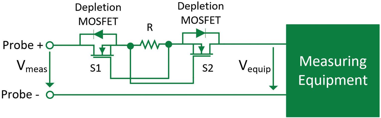
voltage protection circuits. A DM MOSFET can protect measurement instruments from the accidental connection of measurement probes to high voltages. The typical configuration has two MOSFETs configured back-to-back with a resistor in between them. Each MOSFET gate is connected to the source of the other MOSFET. This approach protects the instrument by limiting the current. Bench-top or hand-held instruments a potential applications.
Depletion MOSFETs are also excellent for implementing solid-state relay (SSR) load switching in place of electromechanical relays (EMR). SSRs provide immunity to magnetic fields, high reliability due to the absence


of mechanical contacts, smooth operation thanks to the elimination of contact chattering, and take up less space than EMRs on PCBs. SSR applications include medical equipment, industrial automation, consumer electronics, and measurement and test equipment.


Although DM MOSFETs are almost forgotten, they can be useful whenever there is a demand for current at zero gate voltage. Littelfuse has the widest range of these, from 60 to 1,700 V and is the only manufacturer offering high-current DM MOSFETs.


a high-voltage protection circuit built with a dm mosfet.

ssr circuit employing dm mosfets. references straight facts about linear mosfets and their applications; bodo’s power systems, october 2021
white paper, mosfets withstand stress of linear mode operation, 2021 , littelfuse, inc., www.ixys.com / documents / articles / article_linear_power_ mosfets.pdf


white paper, depletion-mode power mosfets and applications, abdus sattar, ixys corp., https:// www.ixys.com / documents / appnotes / ixan 0063 .pdf


littelfuse dm mosfets, gate drivers; www.littelfuse.com.


POWER & ENERGY EFFICIENCY HANDBOOK
Advanced Driver-Assistance Systems (ADAS) Classroom Whether or not you want a self-driving car, there’s no arguing that most drivers need “assistance”, which makes ADAS a formidable technology. It’s a new learning curve for many, and this classroom is here to help. Neural network software (and the memory to accommodate it), ADAS sensors, LiDAR, are just some of the technologies that allow a car to “see”. How and why? START WITH TUTORIALS IN THIS EE CLASSROOM! Check out our EE Classroom to learn more: www.eeworldonline.com/adas-classroom
calculations reveal the value of efficiency
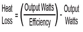
engineers are becoming more sensitive to efficiency when selecting a power supply. Energy flows through the supply, and something less than 100% of that energy can be used because of inefficiencies of power supply components. The difference between usable energy and wasted energy is dissipated as heat. Heat is the enemy because it degrades the components in the power supply and other components in the electrical enclosure.
Suppose we have two power supplies, one 92% efficient, the other 96%. Both sound relatively efficient. Using these figures, we might think that the difference is only 4% (96% - 92% = 4%). But if we have a 100-W power supply, the 92% efficient power supply loses 8 W and the 96% efficient power supply loses 4 W. That is 50% less heat loss from the 96% efficient power supply.
Let’s look at a real-world example using two 480-W power supplies. The PULS CP20.241 has an efficiency rating of 95.6%. A competitive unit recently released has an efficiency rating of 93.1%. The apparent difference is 2.5%. At first glance, not a big deal. But as with the previous hypothetical example, the percentages hide a significant difference in energy use. A 95.6% efficient supply loses 21 W mainly to heat, while
a 93.1% efficient supply loses 33 W, or about 57% more.
A simple method to determine the true difference of heat loss when comparing power supplies is to use the heat loss formula:
Heat is the number one enemy for power supplies because they normally use electrolytic capacitors. Electrolytics have a reputation for exhibiting a short service life when heat is a factor. The most common reason for reduced electrolytic capacitor lifespan is the evaporation or leakage of the liquid electrolyte. Environmental and electrical factors also play a role. Typical environmental factors that can shorten capacitor life include humidity, high temperature, mechanical vibrations, and humidity. Electrical parameters such as applied voltage, charge-discharge duty cycle, and ripple current can also lead to premature failure.
Datasheets define electrolytic capacitor service life under a nominal voltage, nominal current, and upper temperature limit . The temperature, ripple current, and apple voltage can accelerate aging. High temperature speeds the aging of electrolytic capacitors because it boosts the chemical reaction rate. A rise in temperature leads to the gradual evaporation of the electrolyte through the seal.
The life expectancy of an electrolytic capacitor is influenced by the applied voltage as well as the reverse voltage across the cap. Application of excessive voltage across the electrolytic capacitor boosts leakage current. The leakage current is responsible for internal gas generation and self-heating in the capacitor, which ultimately damages the capacitor’s internal structure. Reverse voltage above a few volts causes internal heating and pressure. If an electrolytic capacitor sees high reverse voltage, it may fail from the opening of the safety vent. Ripple current through an electrolytic
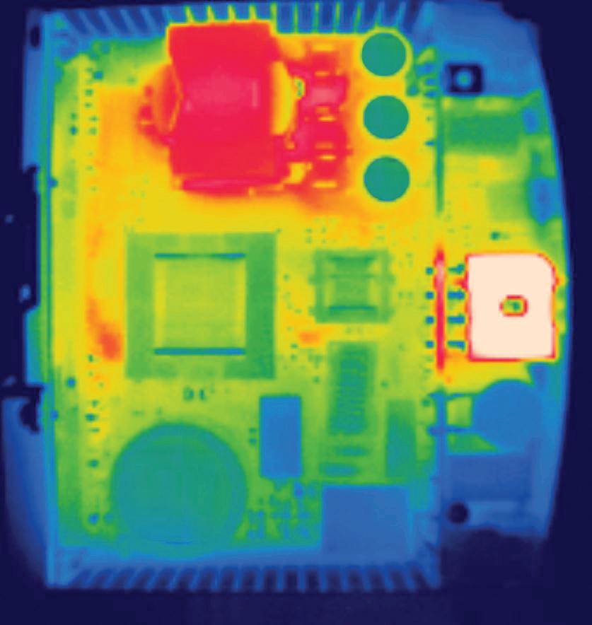
in the thermal image, the larger blue circle at the bottom, and the three smaller blue circles in the upper right are capacitors. those capacitors are positioned so either they reside in a naturally cooler area (bottom), or they are separated by an air channel that protects them from heat and therefore extends their lifetime and boosts their reliability.
capacitor produces more internal heat. Discharge currents are catastrophic to electrolytic capacitor lifespans. The discharge current increases the internal heating and pressure, which reflects as the capacitance value drop during initial stages. With time, the charge-discharge duty cycle may lead to the destruction of the electrolytic capacitor by opening the safety vent to release gases.
The general rule of thumb, as published by capacitor manufacturers, is that every 10°C increase in temperature results in a 50% decrease in life for the capacitor. Since capacitors are so sensitive to heat, a good design will also thermally separate the capacitors from heat producing components like transformers and bridge rectifiers.
In addition to the drawbacks of electrolytic capacitors, often there are far more sensitive electronic components inside an enclosure which can be degraded by heat. In a nutshell, heat can radically reduce the reliability and lifetime of the power supply and other components in the enclosure. In many cases, it can force the use of a larger enclosure, the use of a cooling, or a derating of equipment to compensate for high heat losses.
Thus a power supply with the highest efficiency and good thermal design can mean the difference between a reliable control system and a system where problems ultimately will surface.
Design engineers must also consider the amount of energy necessary to operate the load. Referring to the example of the two 480-W power supplies, we can review them from an energy standpoint. The power supply which was rated 93.1% efficient and had 33 W of lost energy would, from a simplistic calculation, lose 1.65 kW over a 50-hr work week. The 95.6% efficient CP20 supply would have losses of only 1.05 kW. Using an average cost of 13¢/kWh. Thus the less efficient supply would waste approximately $11.16 annually vs. $7.10 annually for the CP20. Multiply this by the number of power supplies in use and the savings can be quite significant over the life of a control system.
references puls l.p., www.pulspower.com
19DESIGN WORLD — EE NETWORK10 • 2022eeworldonline.com | designworldonline.com POWER SUPPLY EFFICIENCY
a few back-of-the-envelope estimates show why it pays to maximize power supply efficiency.
chris harman • puls l.p.
advanced capacitors enable high-efficiency energy scavenging
modern tantalum capacitors and supercapacitors make it possible for compact energy harvesting systems to power iot mcu applications.
advanced
tantalum capacitors and supercapacitors are enabling advanced ICs to be powered by compact and low-cost energy harvesting and scavenging sources. These developments make possible maintenance-free control systems in IoT applications extending from remote monitoring to smart industrial point controllers, wearable electronics, and location tracking devices.
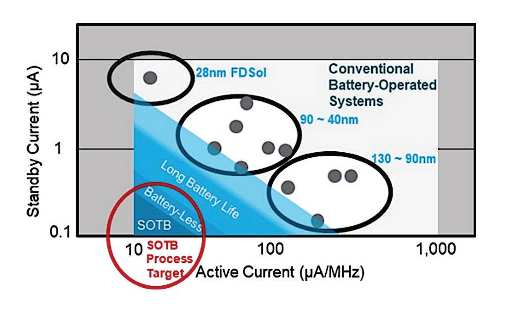
Consider as a case in point the RE family of Renesas MCUs. It is based on the company’s silicon-onthin-buried-oxide (SOTB) process technology which enables ultra-low power consumption in both active and standby modes. RE family MCUs typically consume 25 µA/ MHz when active in internal lowdropout regulator (LDO) mode, 12 µA/MHz in external dc/dc mode, 400 nA in standby with 32 KB RAM retention, and 100 nA in deep
standby. Low current consumption at low voltages allows these advanced MCUs to employ energy harvesting or scavenging power sources rather than traditional batteries or mains.
Each RE01 MCU contains an energy harvesting controller (EHC) equipped with a sub-level PMIC, charge controller, and power management function. These EHCs harvest energy generated from solar, piezoelectric, micro turbine, pressure, and thermal electric generator (TEG) power sources. The MCUs use one of two integrated capacitors to manage, channel, and balance harvested power and MCU power consumption. In this application, the EHCs provide basic functions like reverse-current protection and also act as the direct energy harvesting link. The energy harvesting actions include voltage regulation, quick start-up control, autonomous and reliable startup sequencing, start-up current control, energy storage charge management, and the selection of capacitor power sources.
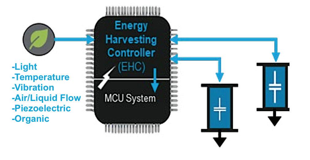
When an RE01 MCU is
ron demcko, daniel west, ashley stanziola • kyocera avx
re 01 microcontroller
an re01 mcu powered by harvested energy.
powered by harvested energy, an advanced tantalum capacitor provides temporary energy storage while a large-valued supercapacitor handles secondary storage. The ultra-low-power MCUs enabled by these advanced capacitors handle control and communication capabilities in IoT applications ranging from remote environmental monitoring and agricultural optimization to asset tracking, wearable electronics, and set-itand-forget-it industrial monitoring.
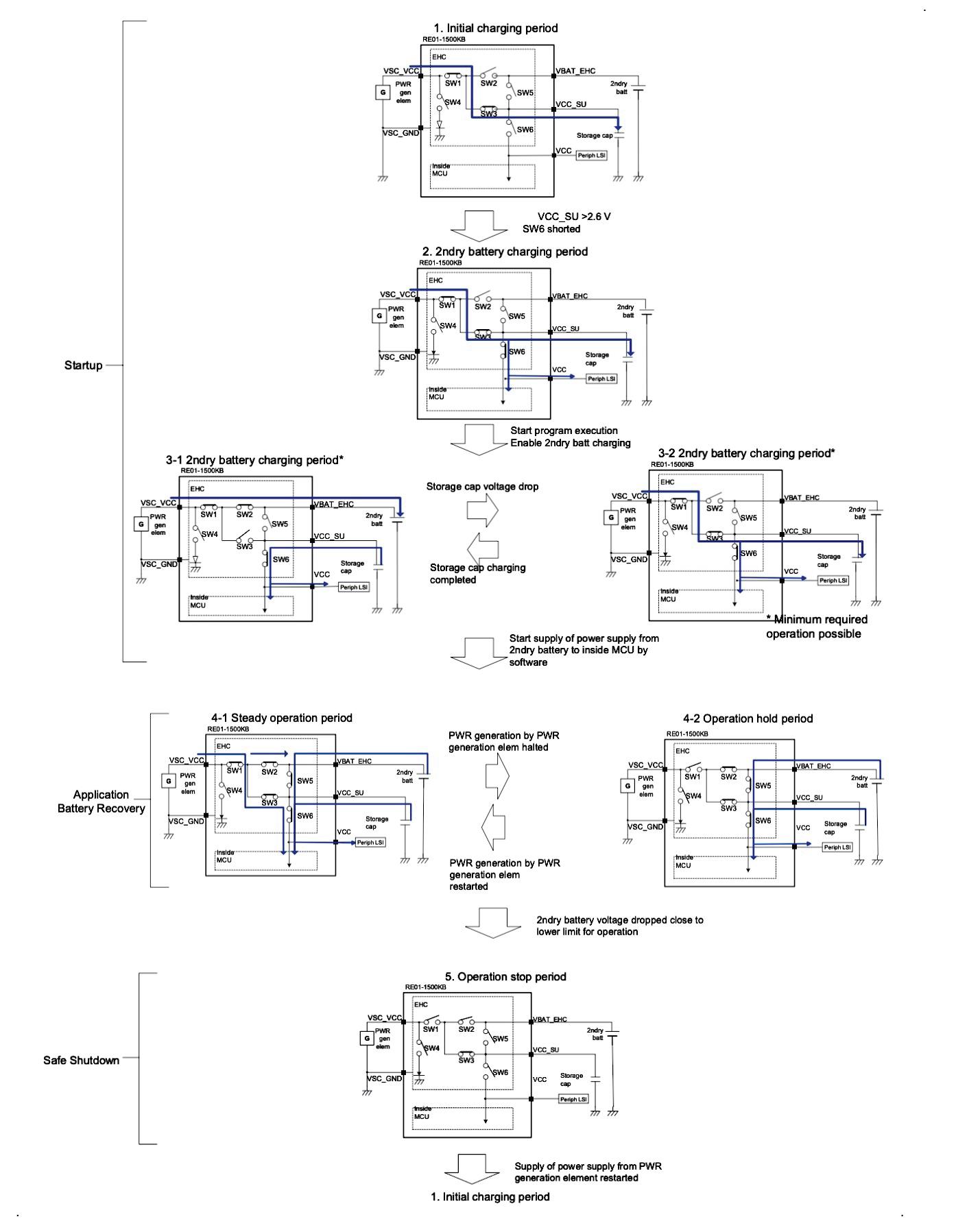
The EHCs in RE01 MCUs configured for energy harvesting rely on a start-up capacitor (C-SU) to charge quickly and to provide the low-level power for MCU power-up initiation. For long-term power, they can use batteries or advanced supercapacitors. Once energy harvesting power is apparent, the EHC charges the C-SU. When C-SU charges to 3.0 V, power-on reset initiates at the MCU and the secondary supercapacitor starts charging.
While the supercapacitor
charges, the EHC uses C-SU power to initiate various MCU operations. Once the supercapacitor has charged, the MCU draws on its energy for longer-term operation. During that time, the C-SU recharges so it can maintain various active computing functions when the EHCs isolate the supercapacitors from the MCU to recharge them. Once the supercapacitors recharge, the MCU again transitions from the C-SU to the supercapacitor power source and, in doing so, enables more of its functions.
This process continues in a loop until the energy harvesting power source is no longer available and the system shuts down. At that point, the MCU waits for C-SU to charge and the use cycle continues.
the start-up capacitor
The C-SU in an energy harvesting MCU must operate from -40 to + 85°C and provide 100–150 µF of capacitance across that
the re01 mcu energy harvesting operation pictured here illustrates the power consumption requirements for sotb technology compared to other competing process technologies, such as fully depleted silicon on insulator ( fc-soi ) processed drives.
20 DESIGN WORLD — EE NETWORK 10 • 2022 eeworldonline.com | designworldonline.com
POWER & ENERGY EFFICIENCY HANDBOOK
the relationship between power management states and the ehc interaction with c-su and the storage supercapacitors.
temperature range. It also must exhibit low ESR (equivalent series resistance) during charging and low leakage current, or high insulation resistance, to reduce standby currents.
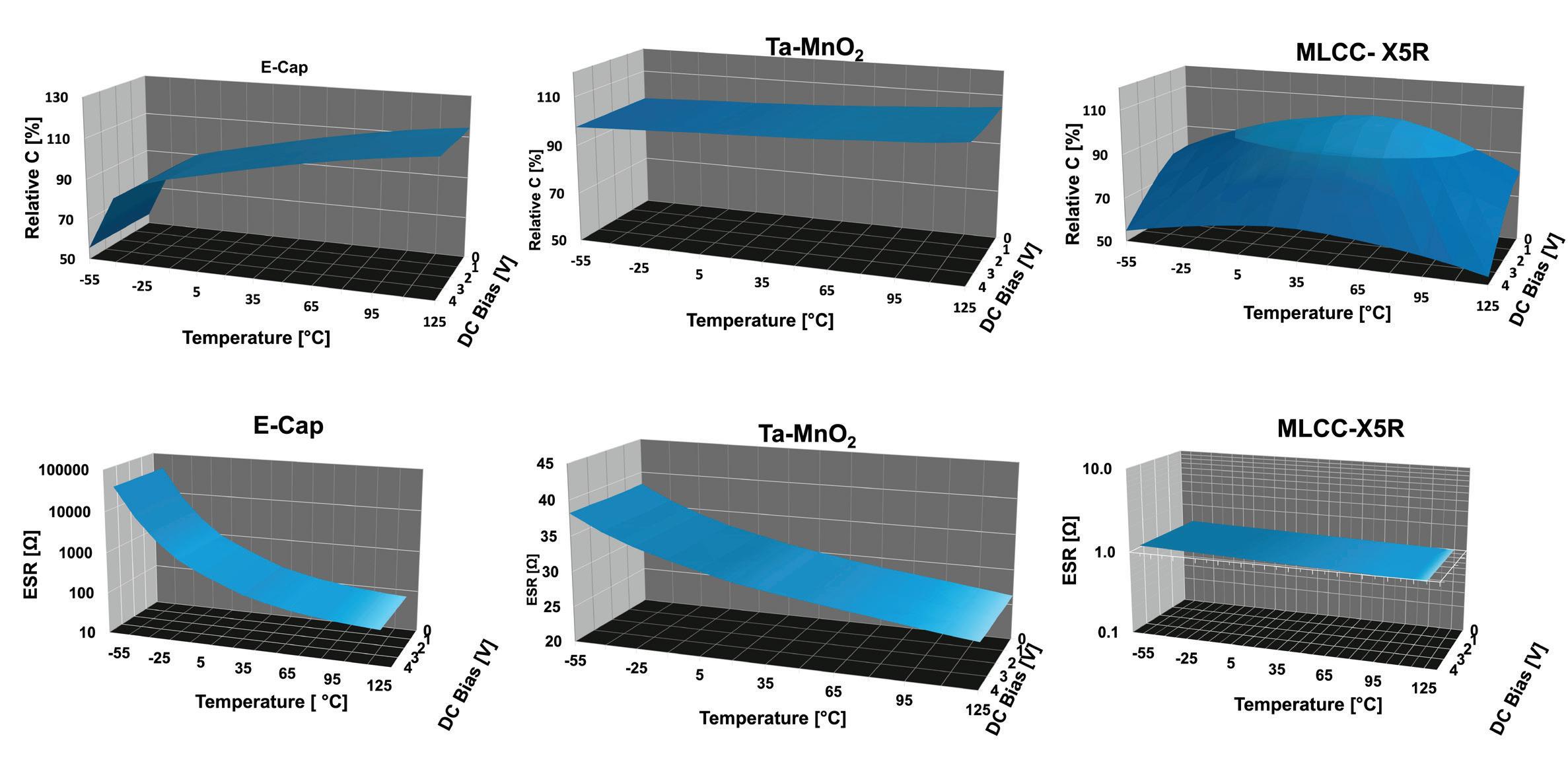
Three different capacitor technologies can exhibit these properties at around 3 V: tantalum, aluminum electrolytic, and multilayer ceramic capacitor (MLCC). Tantalum capacitors best meet the requirements of a start-up charge retention capacitor. Tantalum capacitors have stable values regardless of
dc bias, operating temperature, or age. In contrast, an MLCC rated for 100 µF is likely to only demonstrate 20–30 µF in an application. High-capacitance MLCCs also come in packages larger than equivalent tantalum devices and exhibit extreme capacitance instability. Thus they aren’t recommended for use as start-up capacitors.
Aluminum electrolytic capacitors are more stable than MLCCs but at the price of increased size and weight and potentially much
less reliability. Aluminum electrolytic capacitors squeeze large capacitance values into small packages, but their electrical properties vary with temperature.
Tantalum capacitors are available in numerous case styles, including true EIA case size surface-mount technology (SMT) chips and high-density under-tab styles. They also allow design engineers to further reduce any in-circuit leakage by derating the capacitor voltage rating.
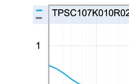
Consider as an example the KYOCERA AVX TPS Series tantalum capacitor (P/N: TPSC107K010R0200). TPS Series capacitors are automotive-grade components qualified to AEC-Q200 and available in 14 different case sizes (EIA 1206 to EIA 2917) with voltage ratings spanning 2.5–50 V and capacitance values extending from 0.15 µF to 1,500 µF. They exhibit ESR as low as 80 mΩ, a maximum direct leakage current of 19.8 μA, and a 12% maximum dissipation factor at 120 Hz. They are also rated for operating temperatures from -55 to +125°C and are suitable for battery support and smoothing/filtering on the 3.3-V power rails frequently chosen for dc/ dc converter output voltage.
supercapacitor selection Supercapacitors (C-Bulk) are widely employed as low-cost alternatives to rechargeable batteries in applications requiring up to around a million charge/discharge cycles. Supercapacitor cycling qualities are well suited for high-frequency charge/discharge applications like energy harvesting MCUs. Supercapacitors are available in multiple form factors, simplifying their integration into a wide variety of end systems. Selection is generally based on a combination of package qualities and the application run time.
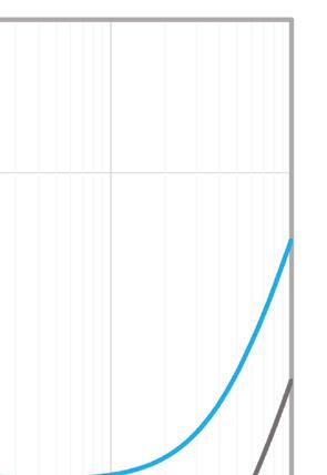
Consider two examples. In the first, two discrete, ultraminiature KYOCERA AVX SCC Series radial-can supercapacitors (P/N: SCCQ12B105PRB) connect in series to create a 0.5-F, 5.4-V storage device. The second example uses a miniature KYOCERA AVX SCM Series supercapacitor module (P/N: SCMR18C105PRBA0) comprised of two packaged, series-connected radial supercapacitors and rated for 1 F at 5V.
Radial-can supercapacitors are commonly used in single configurations for lower voltage designs, but multiple cans can be configured to handle higher voltage loads, as is the case in this study.
Multiple cans can be balanced via active or passive methods. Supercapacitor balancing is
21DESIGN WORLD — EE NETWORK10 • 2022eeworldonline.com | designworldonline.com TANTALUM CAPACITORS
Capacitance
3.2/2.8
1.45/0.90
start-up voltage requirements for and comparative performance of tantalum capacitors, aluminum electrolytic capacitors, and x 5 r mlccs.
necessary to ensure long lifetimes for multiple supercapacitors connected in series. Balancing prevents any overvoltage on one capacitor from damaging any of the other supercapacitors in the stack. Passive balancing uses just a resistor and is the cheapest, smallest, and most user-friendly method. But it also comes with a disadvantage: Power dissipated through the balancing resistor reduces overall efficiency. Active semiconductor balancing is the most efficient and exacting method. However, it’s
stability vs. temperature and bias for tantalum capacitors, aluminum electrolytic capacitors, and x 5 r mlccs
5.5/5.65
µF at -40°C
µF at +85°C
supercapacitors in series and packaging them as a module. This approach packs more capacitance into a given package size and enables higher voltage ratings. These modules can be balanced or unbalanced and feature hard-shell or heat-shrink packaging depending leakage current vs. rated voltage [%]
1.75/1.25
also more costly. The space required for active balancing varies greatly based upon the number of cells and the size of the semiconductors that do the balancing.
The RE MCU example uses SCC Series discrete radial-can supercapacitors. These devices come in 10 different case sizes rated for 2.7 V from -40 to +65°C and 2.3 V from -40 to +85°C. The SCC Series also spans capacitance values of 1–3,000 F, giving designers a high degree of flexibility. Competing solutions are also readily available.
Modular radial-can packages are manufactured by connecting two radial-can
on the application reliability requirements. SCM Series supercapacitor modules have a much larger storage capacitance than the SCC Series and, as such, can power the MCU load for an extending period of time. Regardless of the specific package configuration, supercapacitors must be derated for reliable long-term operation. Studies have
22 DESIGN WORLD — EE NETWORK 10 • 2022 eeworldonline.com | designworldonline.com POWER & ENERGY EFFICIENCY HANDBOOK
Parameter Selection criteria Tantalum Aluminum electrolytic MLCC Capacitance value 100µ target 100µF Operating temperature range -40°C to +85°C -55°C to +105°C -40°C to +85°C -55°C to +85°C
stability 100 µF from -40°C to 85°C ~97 µF at -40°C 102 µF to +85°C ~88 µF at -40°C 105 µF +85°C ~40
40
@ 3V DC Bias Leakage (µA) Lowest better 1.1 µA measured 0.63 μA available 6.3 µA 1.5 µA at 85°C ESR <10Ω 200mΩ tested 45mΩ available 300mΩ 4mΩ PCB pad area used X Y board area mm / Z height 6.2 x
2.2 x
available 6.5 x
3.35 x
Radial can 1F to 3,000F
Radial module 0.33F
Custom module 100s to
15F
revealed that supercapacitor reliability is a function of applied voltage and operating temperature. In tests, various acetonitrile (ACN) chemistry supercapacitors underwent matrix
6.3-60mm dia 12-138mm long
dia, 13.6-32mm W, 14-33mm L
package
options
Solder in Snap in Cylindrical lug Screw in 0.6g to 504g
Radial straight lead Radial bent lead 1.35g to 18g
options Custom
applied voltage and temperature. Results indicate that supercapacitor expected life more than doubles for every 10°C drop below the maximum operating temperature (85°C) and that life expectancies
remains stable, dropping only about 10% from 0 to 40°C. But because their capacitance values are large--around 3 F/ cc—the capacitance drop can be substantial. And because the lifetime of a supercapacitor rises an order of magnitude for every 10°C drop in operating temperature, capacitance-temperature effects are much more of a reliability concern than a minor drop in capacitance.
Generally speaking, supercapacitors perform significantly better at temperature extremes than lithiumion (L-ion) batteries over the mid- to long-haul.
Supercapacitor voltage ratings are commonly ~2.7 V per cell, but they can be stacked or packaged in series to reach higher voltages. The widespread availability of PMICs with cell balancing tends to dictate the economics of single cells configured by end users.
test results: mtff ( in years ) for acn supercapacitors rated for 5 .4 v /5 .0 v at various voltages and temperatures. a comparison of supercapacitor and li-ion battery characteristics.
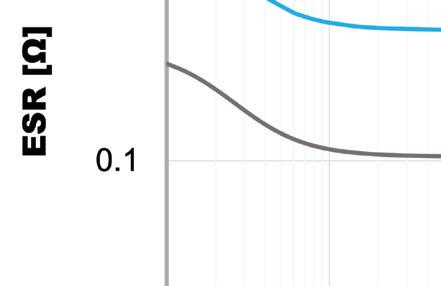
The ESR of supercapacitors can be exceptionally low, down to single-digit milliohm values, depending on the capacitance value and case size of the device. But ESR values rise as temperature drops. At 0°C, ESR values are typically 125% of those at 25°C, and they rise to ~225% of that
In the case of the energy harvesting RE01 MCU application, supercapacitor operating temperatures were about the same as for the RE01, and the cell voltages were adequate. The supercapacitor life cycle exceeded that of equivalent Li-ion batteries.
evident in this simulation of the tps series dut ( p/n: tpsc 107 k010 r 0200) is stable, low-esr performance.
testing with varied voltage, temperature, and humidity stress levels. Researchers measured the capacitance and ESR of the devices under test to determine stress effects. They also tested mean time to failure (MTTF) versus
double with every 0.1-V reduction below the rated voltage.

Three of the most important electrical qualities of supercapacitors are capacitance, ESR, and leakage current. The capacitance of a supercapacitor
around room temperature when near -40°C.
Leakage currents also vary by capacitance value, voltage rating, packaging style, and temperature. Leakage current drops to near zero at around -40°C and rises to ~650% of the 45°C value at ~85°C.
start-up capacitor testing
To demonstrate the use of a tantalum
(C-SU = KYOCERA AVX P/N TPSC107K010R0200), consider two test cases: First, the C-SU used in conjunction with an ultraminiature supercapacitor stack. Second, a
23DESIGN WORLD — EE NETWORK10 • 2022eeworldonline.com | designworldonline.com
a comparison of radial can, radial module, and custom module supercapacitors.
start-up capacitor
Capacitor form factor Capacitance Voltage Dimensions Terminal
Weight
2.7V to 3.0V
to
5V to 9V 6.3-14mm
1,000F 2.7V to ~200V Custom
Custom
Parameter / characteristic Supercapacitor Li-ion battery Charge time 1 to 10 seconds 10 to 60 minutes Charge cycle life 1 million >500 Cell voltage 2.1 to 3.3 volts 3.6 to 4.2 volts Specific energy (Wh/Kg) 5 100 to 200 Specific power (W/Kg) ~10,000 1,000 to 3,000 Charge temperature range -55°C to +90°C 0°C to +45°C Discharge temperature range -55°C to +90°C -20°C to +60°C TANTALUM CAPACITORS
miniature supercapacitor stack but with a larger capacitance value.
Both test cases employ a 256KB RE01 evaluation board in a demo-mode loop. This board can also be powered with a combination of tantalum capacitors and supercapacitors. But the purpose of this test was to confirm that a tantalum capacitor can perform exceptionally well as a C-SU and to identify the operating life provided by the two different-sized (ultraminiature and miniature) supercapacitors.
The C-SU under test — 2.6 mm high occupying a total volume of 0.05 cm3 — takes up just 19.2 mm² of board space. Tantalum capacitors weigh less than competing technologies. This C-SU weighed approximately 170 mg. It also exhibits low and stable ESR. So its size, weight, stability, and reliability make it a good start-up capacitor for low- and ultra-low-power chipsets.
Power from the C-SU properly toggled, and the capacitor worked well in the normal demo mode of the 1500KB RE01 evaluation board. From an energy perspective, the demo execution mode consisted of C-SU charge, power source transition to C-bulk, C-SU secondary charge/maintenance, power transition to C-SU, supercapacitor recharge, and system shutdown cycles.
Two supercapacitor (C-Bulk) test cases provide representative data for end users who
prefer to build their own custom radial stack and for those who prefer to deploy a standard 5.4-V module package. The first test case consists of connecting two ultraminiature radial-can supercapacitors (P/N: SCCQ12B105PRB) in series to build a 0.5-F, 5.4-V rated stack. The second test case consists of a miniature radial module (P/N: SCMR18C105PRBA0) rated to provide 1 F at 5.4 V. (Note: Run-time results will likely vary from data reported here because end-user code and execution cycles won’t be the same as demo mode software.)
Test results revealed that larger C-Bulk devices store more energy and power the MCU longer than start-up capacitors.
Thanks to advanced tantalum start-up capacitors and bulk supercapacitors — energy harvesting generators can handle low-power IoT applications instead of batteries and mains.
To that end, tantalum capacitors exhibit high levels of capacitance stability and low loss in small, lightweight packages and are available in consumer, automotive, commercial off-theshelf, and high-reliability versions suited for the role of a start-up capacitor. The combination of tantalum start-up capacitors and high-energystorage supercapacitors enables the use of energy-efficient MCUs in energy harvesting and scavenging set-and-forget IoT applications.
references demcko, ron, et al., powering iot modules using solar panels, supercapacitors, and an automatic buck/boost controller ic, kyocera avx, 22 jan. 2021 , www.kyoceraavx.com / news / powering-iot-modulestech-paper.
zednicek, thomas, high cv mlcc dc / ac bias aging capacitance loss explained, passive components blog, european passive components institute ( ecpi ) , 23 sept. 2019 , passive-components.eu / wp-content / uploads /2019/10/ high-cv-mlcc-dcac-biasageing-capacitance-loss-explained.pdf.
derose, e., knopsnyder, b., & rawal, b. (2018) , reliability of supercapacitors: unique performance at 85 °c & selfbalancing ( part 1) , kyocera avx. https: // www.kyocera-avx.com / resources / reliability-of-supercapacitors-uniqueperformance-at-85c-self-balancing / derose, e., knopsnyder, b., & rawal, b. (2018) , reliability of supercapacitors: long-term reliability test data ( part 2) , kyocera avx. https: // www.kyoceraavx.com/resources/reliability-ofsupercapacitors-long-term-reliabilitytest-data/
24 DESIGN WORLD — EE NETWORK 10 • 2022 eeworldonline.com | designworldonline.com POWER & ENERGY EFFICIENCY HANDBOOK
a comparison of the two supercapacitor test case specifications. supercapacitor charge / discharge cycles P/N Capacitance Tolerance Voltage Max temp. DCL @72 hrs. DC ESR Diameter Length Max energy (W) SCCQ12B105PRB 1F +100/-0% 2.7V 85°C 6µA 500 mΩ 6.3 mm 12 mm 0.0010 SCMR18C105PRBA0 5V 8µA 720 mΩ 8 mm 18 mm 0.0035


Lessons in Overdesign Cosmonauts used a pencil. PROVEN 40 YEAR BATTERY OPERATING LIFE * Don’t overdesign your battery. Learn more about powering remote wireless devices with simply better batteries that are smaller, lighter, cheaper and last longer. Visit us at www.tadiranbat.com * Tadiran LiSOCL2 batteries feature the lowest annual self-discharge rate of any competitive battery, less than 1% per year, enabling these batteries to operate over 40 years depending on device operating usage. However, this is not an expressed or implied warranty, as each application differs in terms of annual energy consumption and/or operating environment. NASA spent millions inventing a pen that would work in zero gravity. Tadiran Batteries 2001 Marcus Ave. Suite 125E Lake Success, NY 11042 1-800-537-1368 516-621-4980 www.tadiranbat.com Ultra-hard tungsten carbide ball Thixotropicinkinan hermeticallysealedand pressurizedreservoir writes3xlongerSliding float separates ink from pressurized nitrogen gas Stainless steel, precision-machined socket prevents leaks and oozing, yet deliversinstant uniform ink flow
how input high-z technology keeps down adc power and size
muxed sar adcs equipped with high impedance technology can substantially reduce circuit footprint and energy use without compromising performance and accuracy. sanjay rajasekhar, arvind shankar • analog devices inc.
signal chain must be designed to settle the sampling capacitor to the new voltage accurately, within the allowed acquisition time. Traditionally, the solution to this problem has been to use a wideband driver amplifier, coupled with an RC filter.
from the ADC sampling capacitor, and reduce the wideband noise of the signal chain by filtering the noise beyond the required settling bandwidth.
a signal chain with a traditional muxed sar adc.
The sensor could generate a voltage or a current, and the sensor interface circuit could be an instrumentation amplifier or a trans-impedance amplifier, respectively. The capacitor is normally an NP0/C0G type, as other types can cause significant distortion. NP0 capacitors have high linearity but low density.
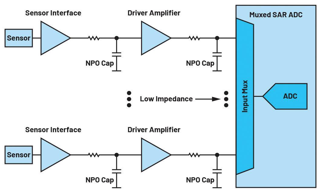
In the traditional signal chain, the designer is forced to use a driver amplifier and a large capacitor for channel. Each driver amplifier could consume anywhere
muxed
successive approximation register analog-to-digital converters (SAR ADCs) find use in applications that must constantly monitor multiple critical variables. In optical communications, laser biasing could be monitored via optical power measurement, while in vital signs measurements, EEG/ ECG signals from electrodes could be monitored.
These muxed applications have some common requirements. Specifically, there are many channels to monitor. Generally, the ADC sequences through all the channels. The channel voltages are generally uncorrelated with each other, and there are tight constraints on the system-level footprint and power.
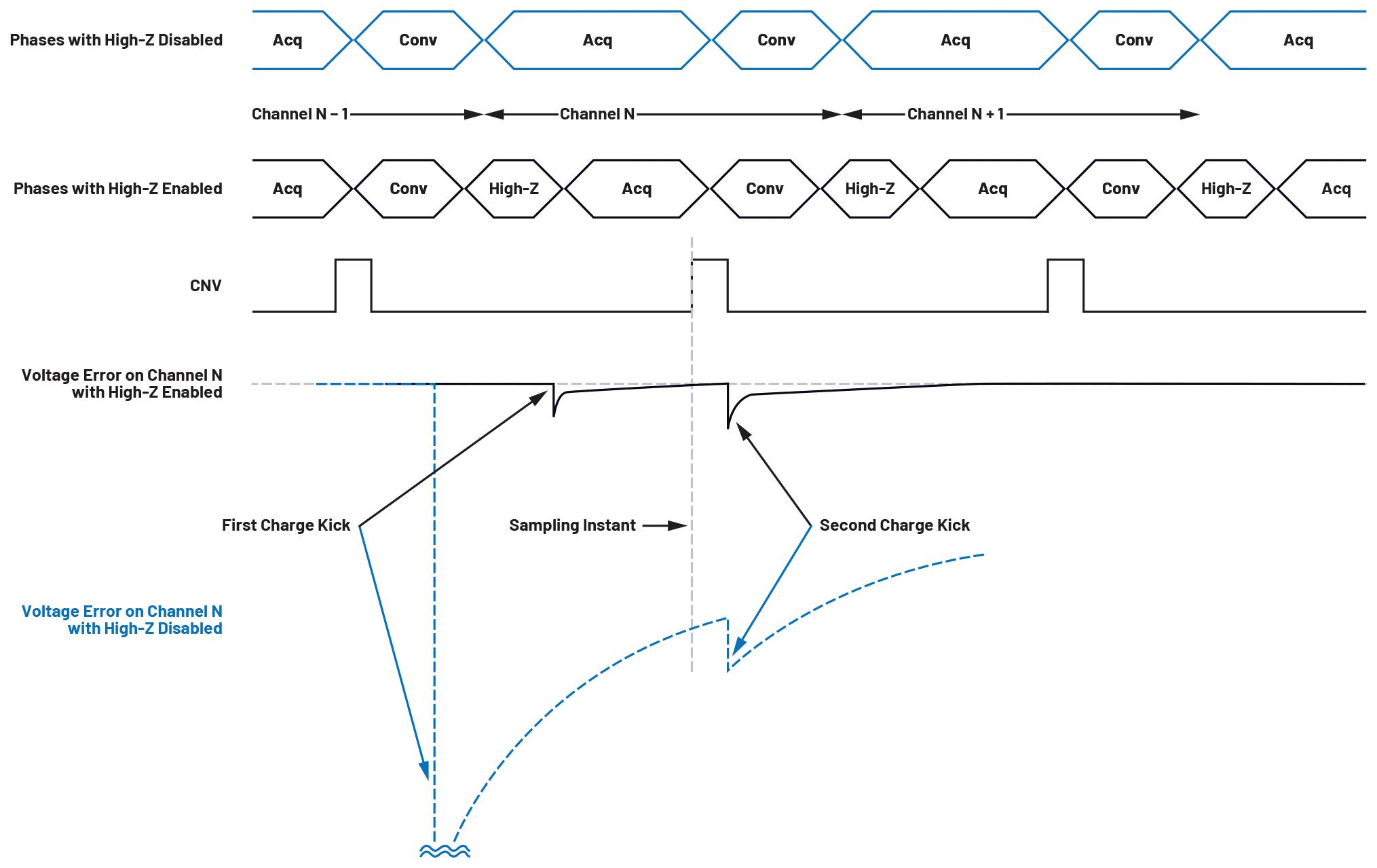
These requirements lead to some challenges. As the ADC finishes a conversion on one channel, the sampling capacitor
within the ADC charges to the voltage of the channel. If the sampling capacitor voltage differs substantially from the voltage of the channel next in sequence, the
The NP0 capacitor is also chosen to be much larger in value than the ADC internal sampling capacitor. It performs two critical functions: Reduce the kickback
phases of the ad 4696 with high-z enabled and disabled. the first rising edge of cnv samples the voltage on channel n – 1 . the voltage on channel n can often be substantially different from the voltage on channel n – 1 , to which the adc capacitor is now charged. this results in a huge voltage kick on channel n ( dark blue dashed line ) and introduces a large error in the channel voltage at the sampling instant ( second rising edge of cnv ) .
26 DESIGN WORLD — EE NETWORK 10 • 2022 eeworldonline.com | designworldonline.com POWER & ENERGY EFFICIENCY HANDBOOK
between tenths of a milliamp to a few milliamps. Each capacitor, including clearances, could take up around 1 mm2 of the board area. Replicating this signal chain over many channels significantly boosts system footprint and power consumption. This constitutes one of the major problems in muxed SAR ADC applications today.
input high-z technology?


The term high-Z technology, in the context of analog input, refers to a collection of circuit techniques that—without consuming static or continuous power—substantially boost the effective input impedance of the ADC. This makes the input of the ADC easy to drive.


Let’s assume the muxed ADC is converting on Channel N – 1 and that the next channel to be converted is Channel N. At the rising edge of convert start (CNV), the channel voltage is sampled. The ADC then converts the sampled voltage on Channel N – 1. After the conversion, with the input high-Z disabled, the ADC proceeds to acquire the next channel in the sequence, which is Channel N.
The voltage on Channel N can often be substantially different from the voltage on Channel N – 1, to which the ADC capacitor is now charged. This results in a huge voltage kick on Channel N and introduces a large error in the channel voltage at the sampling instant (second rising edge of CNV). To avoid the voltage kick, a large external capacitor must absorb the kick and a driver amplifier must supply the necessary charge.
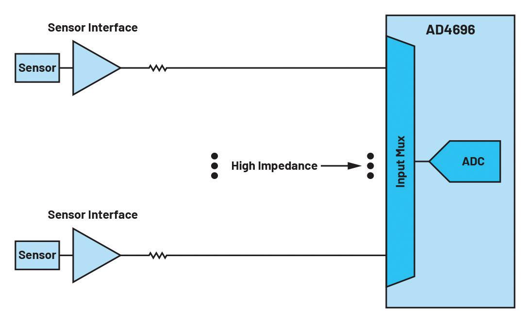
When the input high-Z is enabled, the internal sampling capacitor of the ADC charges up to the voltage on the channel it is going to acquire before the real acquisition begins. Immediately following the conversion on Channel N – 1, a high-Z phase is introduced that accurately charges the ADC sampling capacitor to the present voltage on Channel N. With the capacitor charged, the ADC sampling capacitor doesn’t source any charge and doesn’t result in any kickback when it connects to the external input. In practice, there is usually a small residual error caused by the charge injection of the internal switches (first charge kick). This small residual error results in practically negligible settling error at the sampling instant of Channel N. This charge error with the high-Z enabled would enable a massive improvement in the settling dynamics of the system.

When the sampling on Channel N finishes, the ADC must proceed to do the conversion. So the internal switches disconnect the ADC sampling capacitor from the external input. This results in

CONVERSION POWER EFFICIENCY
27DESIGN WORLD — EE NETWORK a signal chain with the ad 4696 muxed sar adc. Passive Component Power Solutions To learn more about KOA Speer’s Power Solutions, visit KOASpeer.com High Power Cement Resistors BGRV, BWRV, BSRV Up to 40W Surge Current Thick Film Resistors Surge Current Flat Chip SG73 0.1-1W Ultra Precision Flat Chip SG73G 0.2-0.5W Endured Pulse Power SG73P 0.125-1W Endured Surge Voltage SG73S 0.125-1W High-Voltage Thick Film Resistors HV73 Up to 3,000VDC Wide Terminal Resistors WK73 (High Power) Up to 3W
thd vs. number of channels in a sequence. test tone: 1 khz, – 1 dbfs.
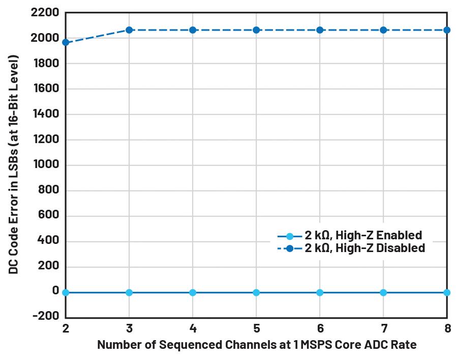
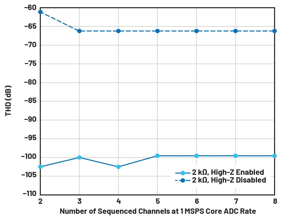
performance, linearity, and accuracy of the signal chain. A small value resistor can help settle sampling charge kicks quickly and thus improve linearity and accuracy. But the improved performance comes at the cost of more overall noise because of a higher effective noise bandwidth. Conversely, a largevalue resistor filters noise better, but at the expense of degraded linearity and accuracy.
noise aliasing. This would necessitate higher resistance values, and the high-Z function helps immensely with maintaining the performance under these conditions.
a second charge kick from the switch opening charge injection. Typically, the second charge kick takes longer to settle, so the magnitude of the first charge kick determines the channel settling error. Thus it is the size of the first charge kick that must be minimized.
The AD4696 latest-generation muxed SAR ADC incorporates input high-Z technology as part of the EasyDrive feature set. As a result, the AD4696 begins acquisition on a channel smoothly. It eliminates the need for a kickback absorption capacitor and a driver amplifier for each channel. The result is a massive reduction of the system footprint and power consumption, as well as a significant simplification of the signal chain.
An important advantage of the input high-Z implemented in the AD4696 family is that the circuits performing the high-Z function can all be power-cycled at the rate of the conversion. So, the power consumption of the high-Z function scales linearly with the throughput of the ADC, just like the core SAR ADC itself. This offers remarkable flexibility compared to the traditional, rather rigid signal chain designs.
The input high-Z function is also built into the LTspice model of the AD4696. The first and second charge kicks are accurately modeled, enabling reliable simulation of the settling artifacts for signal chain designs.
some subtleties
Recall that the NP0 capacitor also provides wideband noise filtering of the signal chain. If we eliminate the capacitor, we must find other ways to filter the noise. One way is to boost the external series resistance. The AD4696 has a 60 pF internal capacitor in series with a 240 Ω typical internal resistor. By setting the external resistor, we can tune the signal chain noise bandwidth to a desired value.
Without the NP0 capacitor, the external resistance plays an important role in the noise
A big advantage of the high-Z technology in AD4696 is that it allows use of large-value resistors (for better noise filtering without degrading the linearity and accuracy. all parameters in the signal chain—noise, linearity, accuracy, power, and solution size.
Measurements have taken place with a 2 kΩ external resistor and without any NP0 capacitor. The results show a massive improvement in ac and dc performance with the analog input high-Z enabled. The experiment involves running the core ADC of the AD4696 at 1 MSPS but increasing the number of channels as part of a round-robin sequence. Data are collected on one channel, while the other channels in the sequence are provided with 0 V inputs.
As the channels are sequenced with the high-Z disabled, nonlinear settling errors arise because the sampling capacitor is not charged to the subsequent channel voltage. This results in significant distortion. With the high-Z enabled, there is a massive improvement in the distortion performance.
Now consider a test where the channel of interest is given a near-full-scale input and the other channels in the sequence are driven with 0 V. Conversions take place on the channel of interest while adding channels to the sequence, and the shift in the average output code from the expected code is plotted.
When operating the core ADC at lower throughputs than 1 MSPS, the user may need to further lower the effective signal chain noise bandwidth to limit the analog front-end
The input high-Z technology implemented in the AD4696 family of parts offers benefits for muxed SAR applications such as reduced system level power, smaller footprint, and fewer components, to name a few, while maintaining high ac performance and dc accuracy. It eliminates the need for a dedicated driver amplifier and a kickback absorption capacitor on each channel. The power consumption for the high-Z function itself scales with the throughput of the ADC, offering remarkable flexibility and versatility for systemlevel design.
acknowledgment the authors would like to thank asif ahmad, peter hurrell, and tyler schmitt for their contributions to this work.
references analog devices inc., www.analog.com
dc steady-state settling errors in lsbs at 16 -bit level with and without the high-z function.
28 DESIGN WORLD — EE NETWORK 10 • 2022 eeworldonline.com | designworldonline.com POWER & ENERGY EFFICIENCY HANDBOOK


it’s the HUMIDITY If it’s not the Heat, cde.com/harsh-environments At 85°C and 85% relative humidity, with rated voltage applied, our new inverter-grade film capacitors are tested 50% longer than the industry standard requirements for Temperature-Humidity-Bias. Improve the reliability of your power electronics design with outstanding capacitor performance at high humidity. Meet the 1,500-hour THB-rated ALH/BLH capacitors 1,500 Hours 1,500 Hours 1,500 Hours 85° C 85°C85%RH 1,500 Hours 1,500 Hours 85°C85%RH 1,500 Hours 1,500 Hours 1,500 Hours 85° C 85°C85%RH 1,500 Hours 1,500 Hours 85°C85%RH AEC-Q200
selecting and applying programmable power supplies
a system-level view of testing is helpful when specifying power requirements.
jeff brakley • ametek programmable power inc.
there are numerous options available for programmable dc power supplies. Users can select from a wide range of voltage, current, and power ratings. Other specifications include input voltage, output voltage regulation, output ripple and noise, and transient response time to a step input. Additionally considerations include digital communications options, software compatibility, and whether there’s a need for manual front-panel controls.
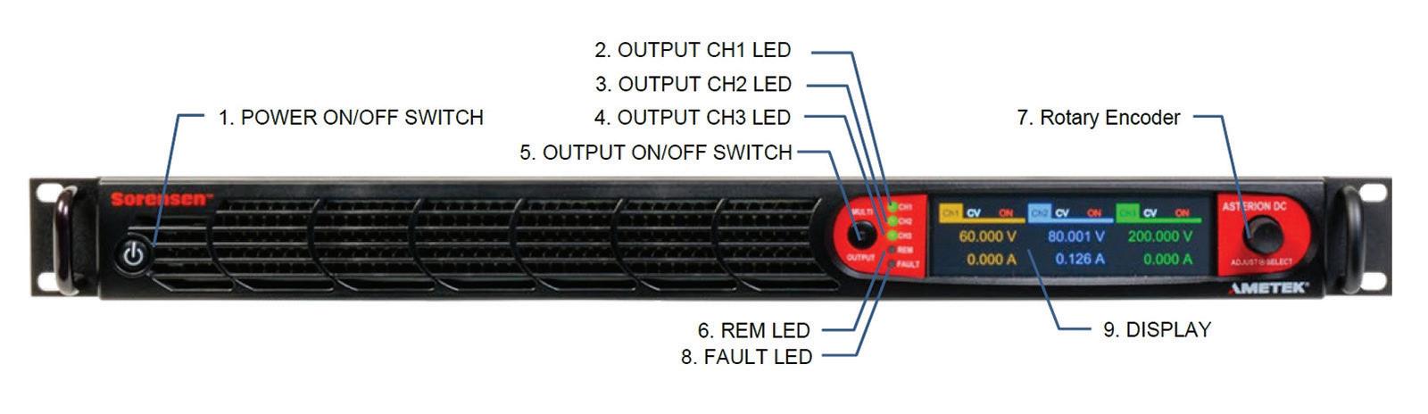
When evaluating applications for programmable power supplies, it is helpful to look at the system as a whole – not just the power supply. A system-level approach helps optimize designs.
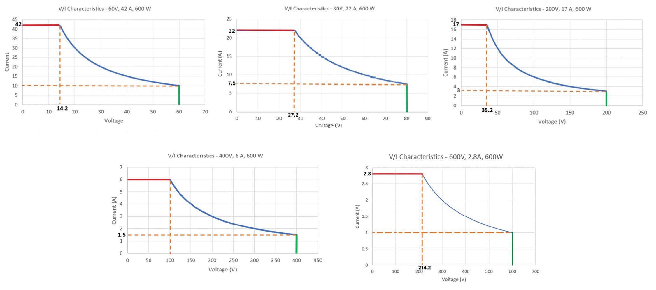
Most operations and systems that require power can be divided into three main types: emulation, stimulus, and process applications. Power emulation applications involve simulating a power source or load to test a product. Here, power supplies or electronic loads might mimic, say, a solar panel or a battery in a testing environment. This procedure lets engineers validate their product and system given the properties of these emulated sources.
One example of a device used in emulation is a solar array simulator (SAS). SASs are power supplies that simulate the power obtained from solar arrays. SASs allow for efficient and economical lab testing of solar-powered equipment such as spacecraft. Spacecraft solar arrays in particular face large solar irradiance and temperature excursions as the amount of sunlight hitting the array changes. They as well experience mechanical changes that accompany aging.
A good SAS can reproduce all possible solar array outputs based on the different input conditions that include orbital rotation, spin, axis alignment and eclipse events,
one aspect of programmable supplies is an autoranging output which produces a v-i curve as shown. this example is from the asterion dc asa Series. maximum output voltage varies inversely with maximum output current to maintain a constant output power. the autoranging feature can be particularly helpful in ate where the required maximum voltage and current ratings may change with successive types of duts.
as well as beginning-of-life or end-of-life operations. Accurate simulation under various space conditions lets system developers comprehensively verify design margins and quickly test spacecraft power systems and any associated electronics. Key qualities to
the front panel of a modern programmable power supply. this example is that of an asa series supply. a point to note is that the display is a touchscreen. the encoder is a selector which, together with the touch screen, allows for control of output parameters, measurements, configurations, and system settings.
30 DESIGN WORLD — EE NETWORK 10 • 2022 eeworldonline.com | designworldonline.com POWER & ENERGY EFFICIENCY HANDBOOK
consider for power simulation systems include peak power tracking accuracy, peak power tracking speed, PV array modeling, and automated test support.
Another example of a power supply used in emulation is the battery string simulator (BSS). These power supplies safely and reliably emulate battery power for spacecraft testing and other demanding applications. BSSs typically operate in either static or dynamic modes. In the static mode, the BSS can instantly produce the terminal voltage corresponding to a particular state-of-charge. When in the dynamic mode, the BSS can charge and discharge energies impressed on the supply, modifying the terminal voltage accordingly. With these two modes, the BSS can easily vary voltage to simulate a battery experiencing charge or discharge, eliminating hours of testing.
Engineers and developers simulating batteries and other types of energy storage will primarily be concerned with constant voltage, power, current and resistance modes; ultra-low voltage operations; sequence simulation; continuous, pulsed and toggled
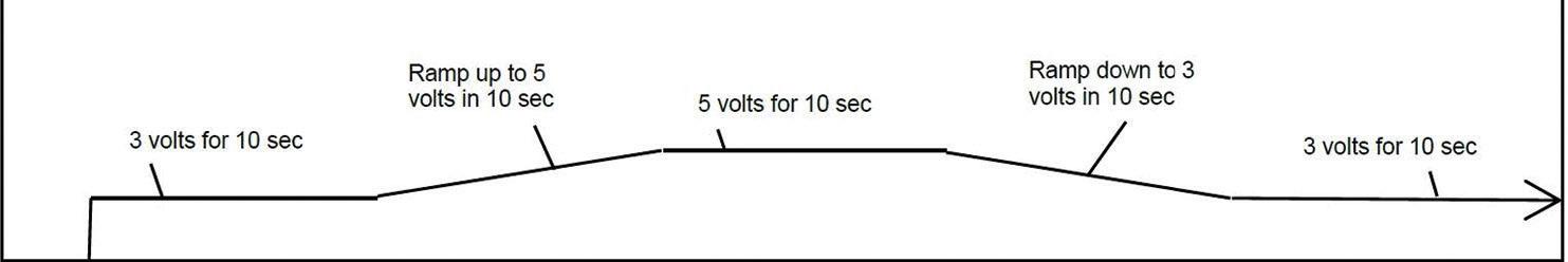
transient simulation; and programmable slewrate simulation.
Basically, a stimulus application involves stimulating a load to do something in response to the input from a power supply. This typically takes place in testing environments. Stimulus applications deal with a wide range of precision ac and dc power sources and eLoads. Every new vehicle has undergone countless product tests during the manufacturing process. Tier One automotive suppliers in particular require fast production without compromising on quality. Automotive research and development labs use power supplies for electronic integration and margin testing.
Researchers require power supplies with a high degree of precision, flexibility and programmability. Commercial and industrial R&D labs utilize power supplies for margin and integration testing of materials, electronics and electrical devices during the development cycle.
Power supplies are the go-to choice for simulating the unique conditions found in space. Power systems and components must perform flawlessly, even when exposed to electromagnetic fields. Similarly, electrical testing
the rear panel of an asa series illustrates the analog and digital interfaces available on modern programmable supplies.
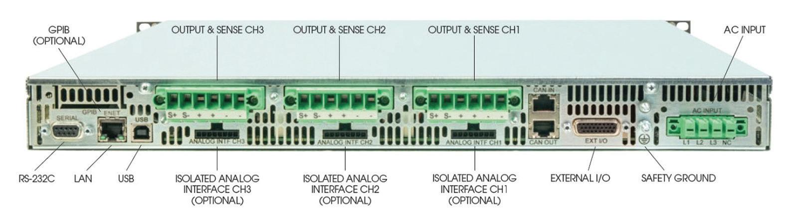
is crucial to military environments. Power supplies are part of the automatic test equipment that is used for electronics repair in military depots.
No matter the industry or specific operation, system developers looking for ac/dc power simulation in stimulus and measurement applications are typically concerned with brown-outs and black-outs, transients, phase loss, frequency variations, and regenerative sink capabilities. On the electronic load side of stimulus power and testing, system developers often must consider non-linear loads, short circuits, high crest and variable power factor simulation, high peak current and low power factor simulation, ultra-low voltage operations, constant voltage, power, current and resistance modes, sequence simulation, continuous, pulsed and toggled transient simulation , and programmable slew rate simulation.
Process applications use power to transform a product. These applications require precise control of the power system. Rather than simulating a device, power supplies in process applications typically serve as loads and stress the system to eliminate infant mortality or early electronic failure.
The nature of process power applications also forces system developers to more heavily consider external simulation. Semiconductor manufacturing and process monitoring is a major process power application. Semiconductor processes such as ion implantation must be tightly controlled to consistently produce reliable and high-quality devices/circuits. Process monitoring allows system developers to detect problems early. Power solutions that enable this process monitoring must be extremely accurate and precise. Similar process power applications include precision reactor heating , oil exploration/recovery, accelerator magnets, and power safety systems.
top, an example of a power output profile that can be set up via commands received over the programmable supply’s remote digital interface. asa and asm series supplies can store 50 sequences of up to 20 commands each. sequences can be comprised of step and ramp functions as well as looping and go-to commands. below, specific sequences can be called as subroutines by other sequences. here, the sequence producing the top trace was called by another sequence for use in defining another sequence. the use of subroutine sequences can effectively enable longer sequences.

An example of programmable supplies designed to handle multiple applications the AMETEK Programmable Power’s multiple output dc programmable power supplies. They include the Sorensen Asterion DC ASA Series and Sorensen Asterion DC ASM Series, which fit in a 1U-high chassis and provide as many as three independent isolated outputs.
The 1U form factor saves space in ATE applications,while the multiple voltages support applications such as functional PCBA test as
31DESIGN WORLD — EE NETWORK10 • 2022eeworldonline.com | designworldonline.com ENERGY EFFICIENT PROGRAMMABLE SUPPLIES
well as burn-in and environmental test. The Asterion DC ASA Series features autoranging outputs in which maximum output voltage varies inversely with maximum output current to maintain a constant-power characteristic. The autoranging feature provides flexibility for ATE systems, in which required maximum voltage and current ratings may change with successive types of DUTs. The five available output channels in the ASA Series follow a 600-W I-V curve, with maximum ratings per channel of 60 V at 42 A, 80 V at 22 A, 200 V at 17 A, 400 V at 6 A, or 600 V at 2.8 A, with the three-output supply offering 1,800 W total output power.
In contrast, the Asterion DC ASM Series features three independent, isolated rectangular output channels. However, the ASM Series does offer higher power ratings at 1,700W per channel for a total output of 5,100 W for a three-channel supply in a 1U chassis. The ASM Series has nine channel configurations offering fixed voltage and current ratings ranging from 40 V at 42 A to 600 V at 2.8 A.

specific applications
Specific examples of how the new supplies are used include a prime contractor awarded an Air Force engineering and manufacturing development contract for a new long-range missile system. Over the course of the multi-year, billion-dollar-plus contract, the application will require a variety of ac and dc Asterion programmable power supplies. Here the ability to combine two ASA units to provide six isolated supplies in a 2U rack height provides considerable space savings.
Another firm in the aerospace industry will use the multi-channel supplies in new automated test systems. Important here was the space savings of three independent, isolated outputs in a 1U rack height, and the long-term reliability and support from AMETEK Programmable Power.
Many features of the ASA and ASM Series help optimize applications for either local or remote control. For local operation, a front-panel touchscreen and an encoder selector button allow users to control output parameters, measurements, configurations, and system settings. From the home screen, users can navigate to several toplevel menus. Dashboard, for example, allows you to change output parameters and view output measurements for each channel .
Programmable functions for the ASA and ASM Series include on/off delays, voltage and current ramps, and sequencing. On/off delays are useful for devices under test such as PCBAs that require multiple voltage sources that turn on and off at different times. ASA and ASM models support delays from 0.1 sec to 100 sec, which are programmable via the Configure Delay top-level menu or by remote control.
The Virtual Panels graphical user interface provides access to sequencing, which is not supported from the front panel. The ASA and ASM Series can store 50 sequences of up to 20 commands each. Sequences can be made up of an extensive list of step and ramp functions as well as looping and go-to commands. One sequence may call another as a subroutine.


references ametek programmable power, www.programmablepower.com


sorensen asterion dc asa series, https: // www.programmablepower.com // products/dc-power-supplies/asterion-dc-asa-series
sorensen asterion dc asm series, https: // www.programmablepower.com / products / dc-power-supplies / asterion-dc-asm-series
POWER & ENERGY EFFICIENCY HANDBOOK
JW SERIES POWER ROCKERS JWM: 10A @ 125/250V AC JWL: 16A @ 125/250V AC JWLW and JWMW: IP67 Rated Panel Seal Versions www.nkkswitches.com | (480) 991 0942 | insidesales@nkkswitches.com | Scottsdale, AZ Designed to handle large inrush current Standard inscription options available
interconnections for
powertrain systems
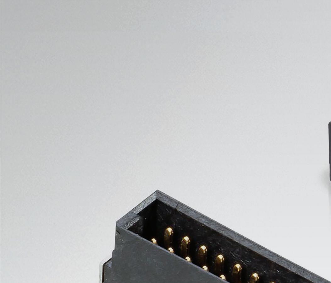
there are six main systems directly associated with an electric vehicle (EV) powertrain. They consist of the onboard charger (OBC), the battery pack, the battery management system (BMS) that monitors various battery pack parameters, the traction inverter that converts dc from the battery into ac that powers the EV electric motor, the motor controller that translates driver commands into changes in the motor torque, and the dc-dc converter that steps down battery voltage for use in functions such as lighting, climate control, infotainment, and so forth.
All these systems are characterized by a heat and vibration environment that can resemble that of conventional motor vehicles. The potential severity of these conditions makes any mechanical systems supporting them critical elements in determining the reliability of the whole vehicle.
With that reliability in mind, consider the electrical connectors found in typical EVs. Several attributes are essential for connectors in any automotive application. First, space is limited, so the dimensions of the connector components must reflect this reality but still offer high contact densities. At the same time, connectors must be able to cope with the demanding automotive environment. They must exhibit resilience when exposed to shocks, vibrations, and high temperatures. Also necessary is protection against dust and moisture ingress.

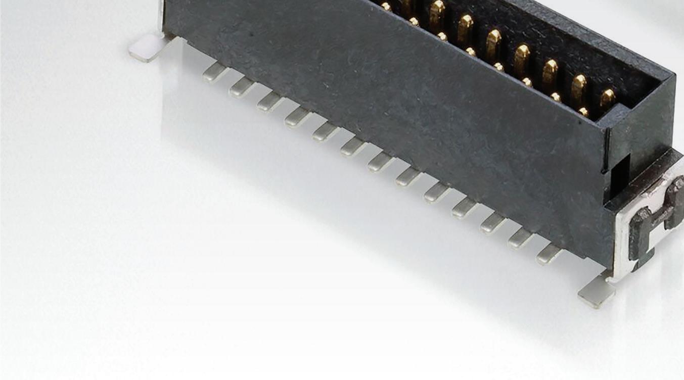

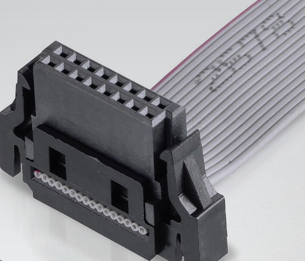
Another feature of modern EVs is a reliance on networking. That forces networking hardware to handle high data rates reliably even in harsh environments. For example, a single radar sensor can generate data at a 15 Mbps rate. A lidar sensor generates 100 Mbps data while a camera can hit 3,500 Mbps. Clearly signal integrity is a must despite
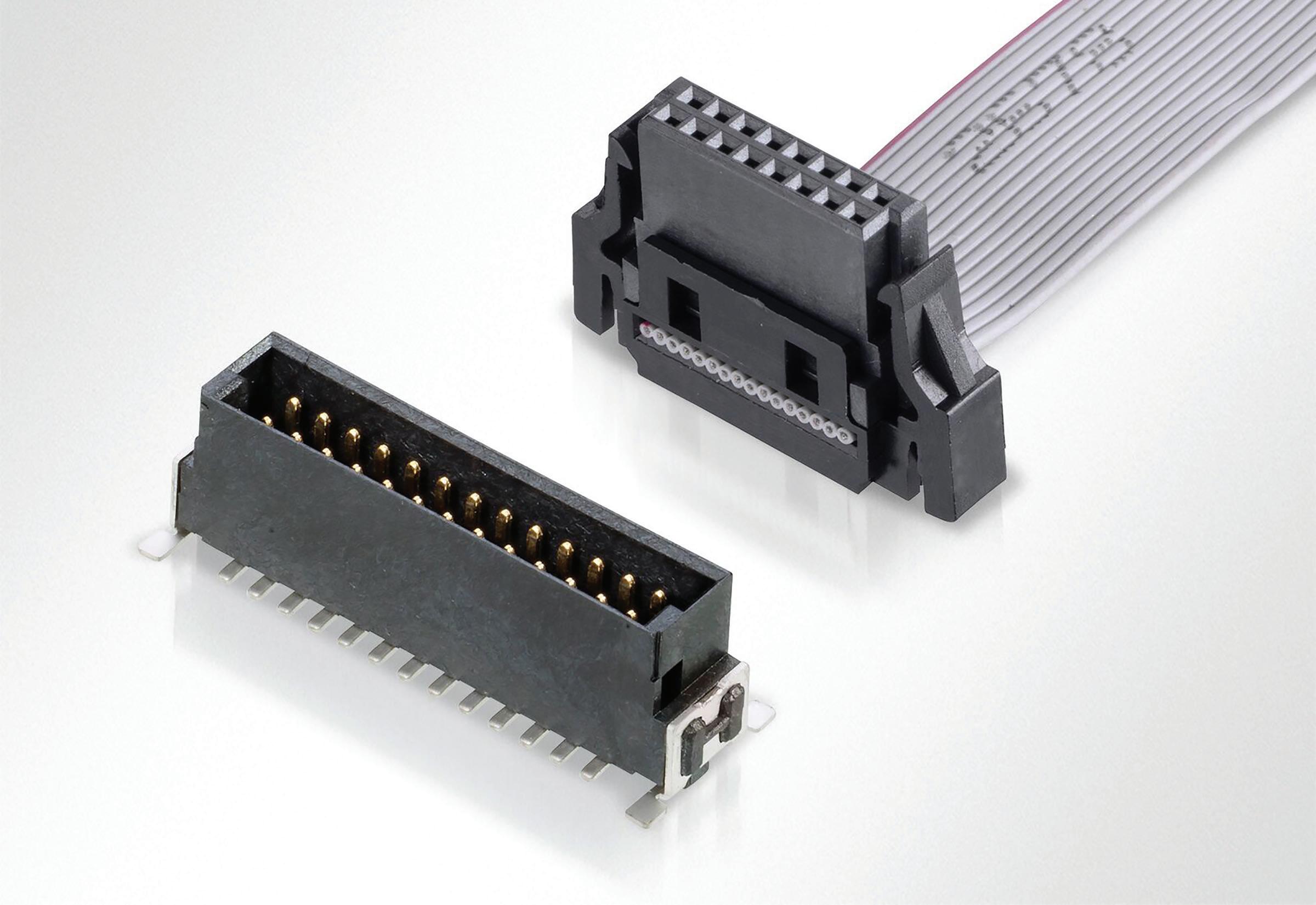
33DESIGN WORLD — EE NETWORK10 • 2022eeworldonline.com | designworldonline.com EV CONNECTORS ev
space constraints that characterize electric vehicle systems put special demands on connectors that must handle high power and rising data rates.
giorgio potenza • harwin
harwin’s
archer kontrol 1 27 -mmpitch connectors supporting 3 gbps. these connectors have been used in ev charging stations and ev inverter control boards, among others.
in an ev power module, the bottom-entry sycamore contact is assembled in an inverted orientation. it becomes ans smt pcb socket with the connections kept away from the lower layers of the assembly.
the electromagnetically noisy environment in which these connectors will function.

In addition, connectors need mechanisms to prevent mating errors during assembly. Finally, the increasingly competitive nature of the EV business means connectors must be competitively priced and not add much to the total bill-ofmaterials costs.


An example of a connector now specified for EV applications is the Archer Kontrol series. These connectors are designed to work reliably in demanding industrial applications. They are 0.05-in, 1.27-mm-pitch surface-mount connectors with SMT solder tabs for added PCB strain relief, and location pegs for accurate placement during soldering.
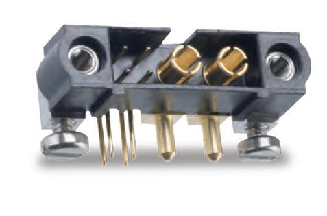
Several manufacturers have

designed Archer Kontrol into their EV powertrains. These highly reliable board-to-board connectors have been integrated into OBCs, motor controllers, and traction inverters. Options for vertical and horizontal orientations enable these connectors to fit into tight spaces.
These connectors are also characterized by a 125°C rating to withstand the heat of powertrain modules and a resilience to vibrations—they are tested cyclically at 10-2,000 Hz, 1.5 mm, 198 m/sec² (20G), for 12 hr. Because they can carry 3 Gbps data rates, they can easily support Ethernet-based in-vehicle networking. Highly durable phosphor bronze contacts with a gold/tin finish are used. These contacts are embedded into rugged plastic housings rated to
UL94V-0 against flammability.
Products in Action
Archer Kontrol connectors are fully shrouded (to prevent damage) and have polarisation built-in to protect against mis-mating. Stacking height options are from 8 to 20 mm and off-the-shelf cable assemblies are available (in 150 and 300 mm lengths), with added latches to provide strain relief.
Electric Vehicle Power Module
Application: Sockets for Insulated Metal Substrate (IMS) PCBs.

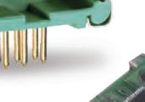


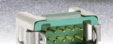
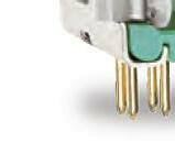
Background:


It is interesting to examine a few automotive applications that now use these connectors. In one formula student car datalogging system, the challenge was to minimize weight while also meeting vibration requirements. And components had to be available off-the-shelf. The team eventually used Gecko (G125 series) connectors for signal pins which provide a low-profile, dual-row interconnect, suited
IMS boards are made with a copper circuit layer on thermally conductive epoxy pre-preg, with an aluminium or copper base plate. Layers are kept electrically isolated (no plated through holes), so standard throughboard sockets are unsuitable.

for stacking and cable mating in areas where PCB real estate is at a premium. Power connections on the car were via Datamate Mix-Tek connections. These handle 3 A per signal contact (all electrically loaded; 3.3 A per individual contact). They have a four-finger contact design to maintain electrical contact through high vibration and shock and employ Beryllium Copper contacts that can handle -55 to +125°C ranges.
Another automotive application involved sockets for Insulated Metal Substrate (IMS) PCBs.

This type of circuit board is common where heat dissipation is needed. Examples include EV management modules and LED light clusters for automotive or street lighting.
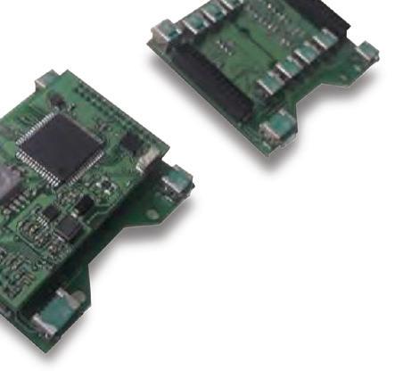
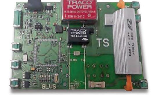
IMS boards are made with a copper circuit layer on thermally conductive epoxy pre-preg, with an aluminium or copper base plate. Layers are kept electrically isolated (no platedthrough holes), so standard
The Challenge:
The customer needed a stand-off socket sitting above the PCB, with surface mount connection to the board. Multiple sockets assemble to pins on a mating panel. The design must be easy to assemble the two boards together, in consideration of Design For Manufacture
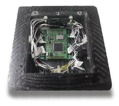
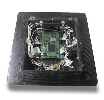
in a data logging system for a formula student car, harwin gecko connections handled signal pins while harwin datamate mix-tek connections handled the power pins.
Products
Autosport
Application: Formula student


Background: Student team student car. (steering wheel, to achieve
The Challenge: Minimise weight. the shelf and Harwin Solution: Gecko for pins. Met the

34 DESIGN WORLD — EE NETWORK 10 • 2022 eeworldonline.com | designworldonline.com POWER & ENERGY EFFICIENCY HANDBOOK
Terminal pin shown in red for demonstration only
through-board sockets are unsuitable. This type of circuit board is common for applications that need heat dissipation such as EV power management modules and LED light clusters.
In the automotive application, the need was for a stand-off socket sitting above the PCB, with a surface-mount connection to the board. Multiple sockets assemble to pins on a mating panel. And the connectors had to make it easy to connect two boards together.


The application used a bottom-entry Sycamore Contact, a design that features three points of contact, providing continuity and ruggedness once only available from two-piece assemblies. A point to note is that the Sycamore connectors are available on tape and reel whereas two-piece assemblies rarely are. The Sycamore Contact is a single-part SMT socket featuring a low profile of only 0.43 mm max above the PCB. Available in top and bottom entry versions, it accepts 1 or 1.5-mm-diameter pins and is open-ended, so mating pin depth is not limited. Manufactured from Beryllium Copper, contacts are goldplated for high conductivity and durability over a temperature range of -50 to +125°C.
In the automotive application the connector is assembled in an inverted orientation. The connection becomes an SMT PCB socket with the solder connections kept away from the lower layers of the assembly. No plated-through hole is required, just a clearance hole under the socket to allow for the length of the terminal pin. The final assembly is easy to mate with the opposing PCB and terminal pins, making subassembly during production fast and simple. If modules are damaged during testing, new modules can be quickly exchanged without any soldering or pressfit issues.
There are a couple other EV applications worth reviewing. In


one case, chargers for public parking bays required a rugged design to handle long-term environmental exposure such as heat, cold and humidity. Easy maintenance also a factor as was board-to-board spacing. Here, Archer Kontrol connectors handled the task, and at the right mated height. In another EV drive system, control boards in the inverter required board-to-board connections that were durable and that could work over a wide temperature range while being priced competitively. Archer Kontrol connectors handled the need thanks to their high temperature ratings and vibration resistance.
references harwin inc., www.harwin.com
EV CONNECTORS
improving battery power efficiency for i o t devices
nanopower ship mode and sleep mode can be optimized to reduce power consumption. suryash rai • analog devices inc.
in the connected world of the internet, power management is an important way to boost the efficiency of IoT applications. In most situations, the sensor node (data acquisition element) sits in a remote area and is powered by a battery. Battery life depends on the efficiency of power strategies for the sensor node. Most of the time, the sensor node stays in sleep mode and switches to active mode only when it must acquire data. The duty cycle of sensor node devices is low. Thus to maximize the battery life, the best strategy is to reduce the sleep current.
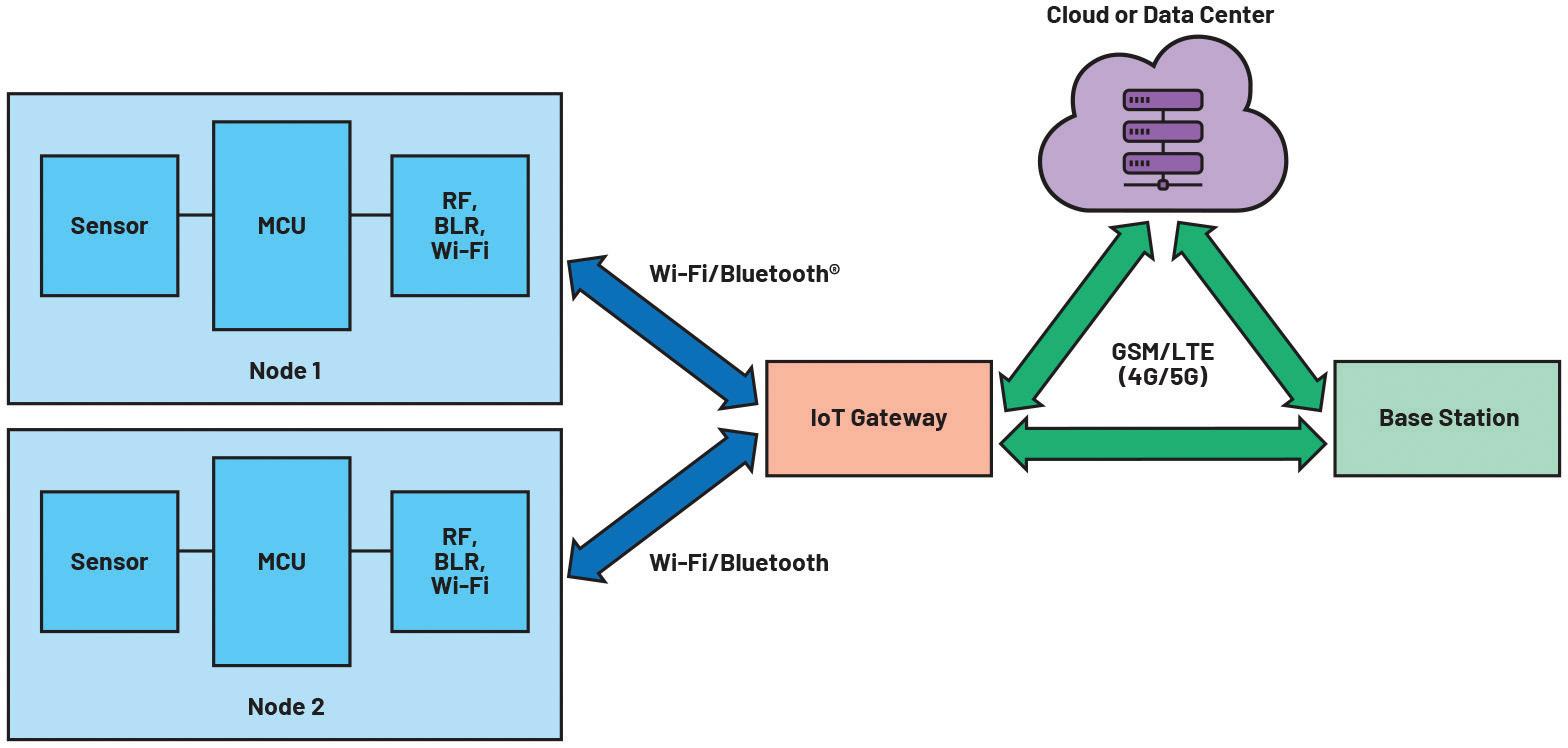
Because overhearing (that is, when a sensor node receives a data packet destined for other nodes in the network) and idle listening are major sources of energy waste in the sensor node, we can evaluate a wireless sensor node’s power consumption using three different areas: the sensor, the microcontroller, and the radio operation.
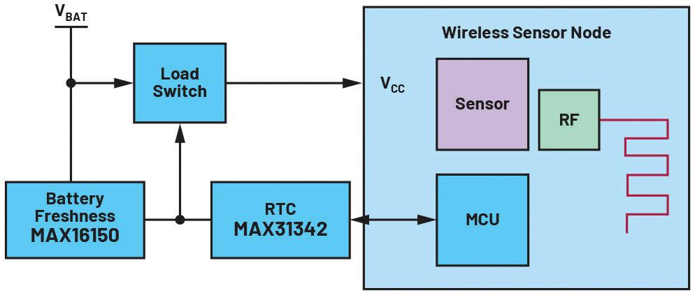
The sensor collects raw data like temperature and humidity and sends it to the MCU. The MCU processes the raw data and transmits it to the cloud or data center via a radio link. However, typical sensor applications operate at extremely low duty cycles (ranging from 0.01% to 1%) and are idle most of the time. So adopting a power management scheme that keeps sensor node sleep current ultralow will conserve battery life. An example would be a smart irrigation system where the sensor node measures the soil moisture and collects data only hourly.
The ship mode and sleep mode are common jargon used in battery-operated IoT devices and are crucial aspects of power management. The ship mode is a nanopower state that prolongs battery life during the shipment stage of a product. In ship mode,
the battery is electrically disconnected from the rest of the system to minimize power drain while the product is idle or unused. Pushbuttons release the ship mode and start the normal operation of the device.
Once the device is active, sleep mode serves to extend the battery life. In sleep mode, all the peripherals of the system are either shutdown or operating at minimum power. IoT
devices wake up periodically, perform a specific task, and then return to sleep mode.
Different sleep modes are realized by disabling various peripherals of the wireless sensor node. For example, in modem sleep, only communication blocks are disabled. In light sleep mode, most of the blocks—including the communication block, sensor block, and digital blocks—are disabled. In deep sleep mode, the wireless sensor node is completely powered off.
Enabling the deep sleep mode in the sensor node can maximize the battery life.
a block diagram of an iot node employing a max 16150 and max 31342 . the max 16150 is an extremely lowpower, pushbutton, on / off controller with a switch debouncer and built-in latch which also serves as a battery “freshness seal” which disconnects a backup battery from any down-stream circuitry until v cc is applied the first time. the max 31342 is a low-current real time clock, rtc.
36 DESIGN WORLD — EE NETWORK 10 • 2022 eeworldonline.com | designworldonline.com POWER & ENERGY EFFICIENCY HANDBOOK
the typical building blocks of an i ot system.
an i ot node
the max 16163 . the max 16163
controllers
switch
max 1616
programmable sleep time.
output, which
Thus optimizing the deep sleep current is the only way to improve the overall battery life.
the duty cycling method
Duty cycling in the IoT module is a widely used technique for enabling deep sleep mode. While a wireless sensor node is in deep sleep, most of the peripherals are off or in shutdown mode, consuming only new nanoamperes. A time-keeping device like the real-time clock (RTC) will wake up the IoT module after a programmed timeout. In this technique, the microcontroller is completely off while the system is in deep sleep mode. However, after recovery, there is always a start-up boot time that will add an undesirable delay. Given this tradeoff, the impact of the proposed principle depends on the qualities of each node and the duty cycle of the application.
The conventional approach for
sleep mode and ship mode is through use of an RTC,
are nanopower
devices
load switch, and push-button controller. Here, a load switch and an RTC are used to power the wireless sensor node on/off. In this approach, only the load switch
An external push-button controller can be connected to a load switch to enable the ship mode feature. The external pushbutton will take the IoT device out of ship mode and put the wireless sensor node into normal operation.
MAX16163/MAX16164 are Analog Devices’ nanopower controllers with on/off controllers and programmable sleep time. The devices integrate a power switch to gate an output, which provides up to 200 mA load current.
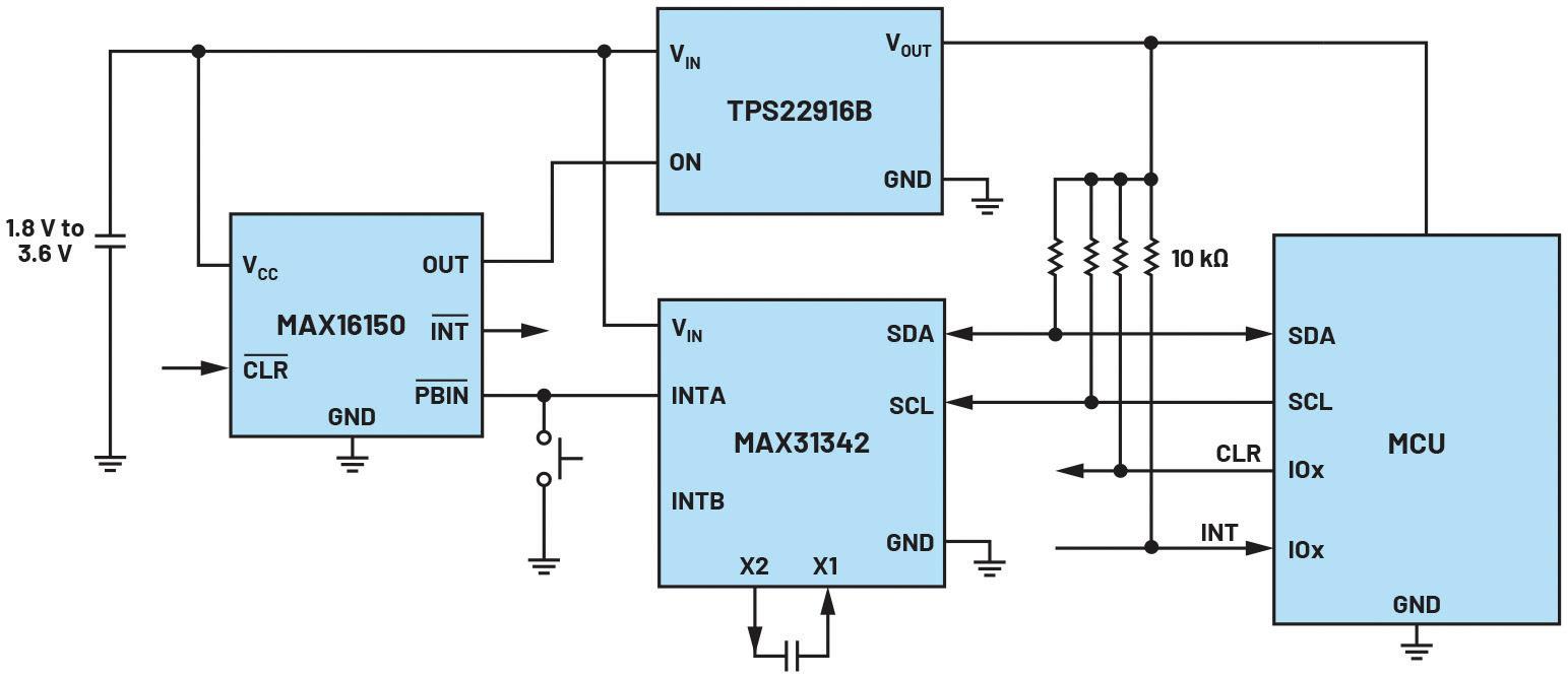
The MAX16162/MAX16163 can replace the conventional load switch, RTC, and battery freshness ICs to reduce BOM counts and costs. The wireless sensor node
of the solution, consider a system containing a MAX31342 RTC (which draws the industry’s smallest quiescent current), battery freshness seal MAX16150, and tiny load switch TPS22916. The RTC is programmed using I2C communication that sets the sleep time of the IoT application. When the timer expires, the interrupt signal pulls down the PBIN pin of the MAX16150, which sets the OUT high and turns on the load switch. During the sleep time, only TPS22916, MAX31342, and MAX16150 consume power system power.
Suppose we compare the performance of the conventional
a schematic for an i ot node employing an mcu, low-leakage load switch ( tps 22916) , and max 16150 and max 31342 parts.
and RTC are active, reducing the total quiescent current to nanoamperes. The sleep time can be programmed with the MCU inside the wireless sensor node.
unit connects to the battery via the MAX16162/MAX16163. The sleep time can be programmed by the MCU or can be set using an external resistor from PB/SLP to the ground or using the I2C command from the MCU. The external pushbutton is used to exit the device’s ship mode.
The performance of both schemes depends on the duty cycle of the IoT application. In an application with a small duty cycle, the sleep current is a measure of how efficient the system is when the IoT device is running. The shutdown current is a measure of ship mode power consumption.
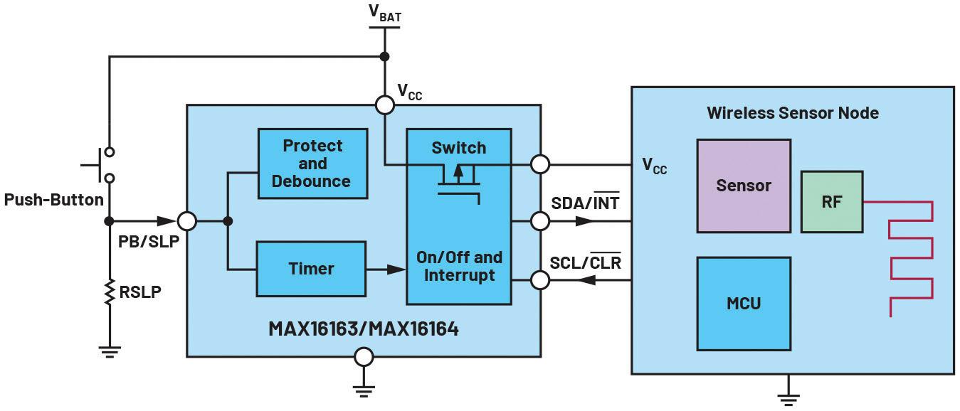
To demonstrate the mode
battery life estimate
battery life vs. duty cycle of a wireless sensor node.
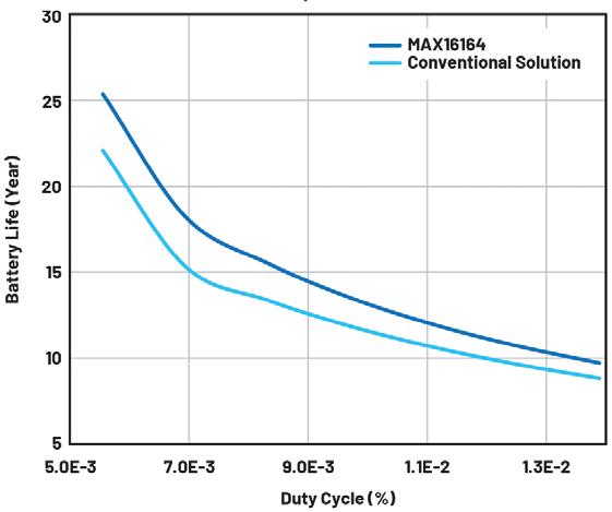
deep
37DESIGN WORLD — EE NETWORK10 • 2022eeworldonline.com | designworldonline.com BATTERY POWER Functional Block Part Number Sleep Mode Current (nA) (Typ) Shutdown Current (nA) (Typ) RTC MAX31342 150 6 Load Switch TPS22916 10 10 Battery Freshness MAX16150 10 10 Total System Current (Typ) 170 26 current consumption by different blocks in conventional approach
using
and
4
on / off
with
the
integrate a power
to gate an
provides up to 200 ma load current.
vs improved approaches under fixed duty cycles using the MAX16163. The lifetime of the battery can be calculated using the average load current
battery capacity.


The average load current can be calculated using the duty cycle of the system.

current is the system current when the wireless sensor node is active. To compare the two approaches, assume the system wakes up once every two hours, performs the specific task, and enters sleep mode after. The system active current is 5 mA. The battery life depends on the duty cycle of the operation.
The MAX16163 from ADI enables a design with a more precise control. It extends battery life by about 20% (for a typical 0.007% duty cycle operation) and reduces the device size to 60% of that required in a conventional approach.


POWER & ENERGY EFFICIENCY HANDBOOK
and
Active
Specification Discrete Solution Using MAX31342, MAX16150, and TPS22916 Integrated Solution MAX16163 Coin Cell Capacity 250 mAh 250 mAh Shutdown Current 146 nA 30 nA Sleep Current 170 nA 10 nA Number of ICs 3 (RTC + load switch + battery freshness) 1 (MAX16163) Crystal Oscillator Required Not required Solution Size 130 mm2 (typical) 50 mm2 (typical) comparison of two different approaches references analog devices inc., www.analog.com sorbothane.com 800.838.3906 SORBOTHANE ® MADE IN THE U.S.A. PROVEN SHOCK, VIBRATION & NOISE REDUCING SOLUTIONS MATERIAL STANDARD PRODUCTS GUIDE OVER 600 PARTS Sorbothane_DesignWorldAd_8-2020_B.indd 1 8/18/20 11:24 AM 38 DESIGN WORLD — EE NETWORK
Emile Berliner receives the patent for the gramophone. James Blyth builds the first electricity generating wind turbine.

commitment to exceeding expectations and keeping the customer at the center of its business philosophy.

Sager Electronics, a TTI Inc., Berkshire Hathaway Company


www.sager.com | 1.800.724.8370

1887
vertical power delivery enables cutting-edge processing
ajith jain • vicor corp. new architectures deliver more efficient power for today’s unprecedented high-performance computing demands.
high-performance
artificial intelligence (AI) processor power levels continue to rise and core voltages are declining with advanced process nodes. These developments are challenging power system designers with managing ever-rising power delivery network (PDN) impedance voltage drops, voltage gradients across high-current, low-voltage processor power pins, transient performance specifications and power loss.
Consider the case of clustered computing, where tightly packed arrays of processors boost the speed and performance of machine learning. PDN complexity rises significantly as current delivery must take place vertically from underneath the array. Designing a PDN using the Vicor Factorized Power Architecture (FPA) with current multipliers at the point-of-load, instead of legacy voltage averaging techniques, allows a significant step up in performance. This is thanks to the qualities of point-of-load (PoL) power components: high current density, reduced component count and importantly, flexible placement. PoL power components thus enable the delivery of current laterally and/or vertically to AI processor core(s) and memory rails, significantly minimizing PDN impedances.
Modern day GPUs have tens of billions of transistors. Better processor performance comes at the price of exponentially rising power demands. In most cases, power delivery is now the limiting factor in computing performance. Power delivery entails not just the distribution of power but also the efficiency, size, cost and thermal performance.
Peak current demands of up to 2,000 A are now a typical requirement. In response, some xPU companies are evaluating multi-rail options where the main core power rails are split into five or more lower-current power inputs. The PDN for each of these rails must still deliver a high current while also undergoing individual tight regulation, which puts pressure on the density of the PDN and its physical location on the accelerator card.
To further add to this complexity, the highly dynamic
nature of machine learning workloads result in high di/dt transients lasting several microseconds. These transients create stress across the PDN of a high-performance processor module or accelerator card.

The work by the Open Compute Project (OCP) consortium has helped establish a framework of standards for designing rack- and card-based processor developments. The Open Rack Standard V2.2 defines a 48-V server backplane and a 48-V operating voltage for open accelerator modules (OAMs) used predominately for AI and machine learning workloads. To maintain compatibility with legacy 12-V systems, the standard stipulates the ability to meet 12-to-48-V and 48-to-12-V requirements.
The technical advances just highlighted focus on the downward trend of voltage scaling, the requirement for tight core voltage tolerance and the upward trend of current consumption. At the board level, the impact of these factors manifests in multiple ways.
The peak current densities encountered are extreme for any PCB. The task of routing power paths capable of handling these huge loads demands careful attention. Highly dynamic workloads can create spiking voltage transients, which sophisticated processors find disruptive and potentially damaging. Yet, a processor board has hundreds of other passive components, memory and other ICs essential to its operation that also need placement.
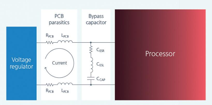
Then there are the I2R losses. Power path trace
the architecture of a typical high-performance processor pdn.
40 DESIGN WORLD — EE NETWORK 10 • 2022 eeworldonline.com | designworldonline.com
POWER & ENERGY EFFICIENCY HANDBOOK
the dramatic increase in current requirements arising from reduced transistor geometry and core voltages.
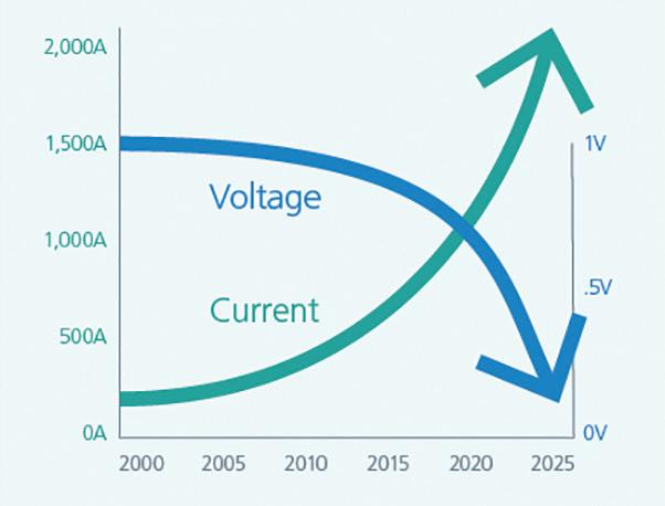
lengths must be short, so the power conversion modules should be close to the processor. The processor load currents and localized thermal gradients of the processor can also flex the PCB, forcing use of board stiffeners. Additionally, the converter’s power efficiency specification should be as high as possible to help mitigate thermal management challenges.
New ideas, architectures, topologies and technologies provide a path to a more reliable, scalable PDN. The Vicor Factorized Power Architecture (FPA) is the foundation for delivering more efficient power for today’s unprecedented high-performance computing demands.
The Vicor FPA divides the task of a power converter into the dedicated functions of regulation and transformation. Separating the two functions allows both to be optimized individually to foster high efficiency and high density. FPA in conjunction with the Sine Amplitude Converter (SAC) topology underpins several innovative power architectures that can help unleash today’s high-performance processors.
Lateral power delivery is an innovative technique where the two current multipliers
(Vicor VTM modules) flank the north and south side or the east and west side of the processor. This technique is preferable for load currents of ~800 A at 0.8 V nominal with an associated 70 µΩ of PDN at 100°C. This architecture is excellent for powering graphics accelerator cards (OAM or otherwise), networking ASICs and APUs used in hyperscale data centers or supercomputer cabinets.
The Lateral-vertical power delivery technique resembles lateral power delivery but with this difference: Only 70% of the power is delivered laterally using the current multipliers that flank the sides of the processor. An additional current multiplier on the bottom side of the processor delivers the remaining 30% of the load current directly to the processor BGA. The hybrid of lateral and vertical reduces PDN loss by almost a factor of four! This technique also frees board space to accommodate a second high-current rail (aux) or HBM memory rails on the top side of the board around the processor.
Vertical-lateral power delivery, on the other hand, pushes >50% of the load current through additional current multipliers on the bottom
design guide on Bluetooth & Connectivity

The demand for high data throughput, low power, and longer battery life is driving much of the breakthroughs and evolutions in connectivity technology.
In this Design Guide, we present the need-to-know basics, as well as the technology fine points aimed at helping you and your designs keep pace and stay competitive in the fast-changing world of connectivity.
HPC POWER DELIVERY
progression of cpu / gpu / asic / fpga peak current requirements
BROUGHT TO YOU BY: find this design guide and more in EE WORLD’S learning center: www.eeworldonline.com
side of the processor. This technique enables a further halving of PDN loss compared to the lateral-vertical approach. A 1,200-A design can now realize a PDN resistance of a mere 10 µΩ, resulting in fewer than 14.4 W of power loss. In this case, heat sinks can cool both the top and bottom sides of the load as space permits. This architecture is especially effective for applications that must accommodate high-speed signal routing from the periphery of the ASIC on the top side of the board and thus cannot afford to host power components there. Examples are CPO, NPO and networking / broadband communication devices.
Vertical power delivery is the ultimate way of delivering high current at low processor core voltages with the lowest PDN resistance. In this case, current multipliers and bypass capacitors are stacked on each other to form an integrated power module (geared current multiplier) that can mount directly underneath the processor by displacing the bypass capacitor bank. Vicor GCMs are custom-built devices that map the current multiplier pinouts to the AI processor BGA and in addition, can provide all the bypass capacitor needs within the module itself. This technique opens up the top floor of the PCB for high-speed signal routing from the periphery of the processor.
factorized power architecture ( fpa ) factorizes the power into dedicated regulation and transformation functions. both these functions can be optimized and deployed individually to provide high density and high efficiency.
Applications such as CPO (co-packaged optics, networking processors) and high-speed signaling ASICs can take advantage of this power delivery technique.
The Vicor architectures are flexible enough to be adapted in a wide variety of high-performance computing scenarios. Vicor architectures can reduce motherboard resistances up to 50x and processing power pin count more than 10x. Leveraging an FPA, Vicor minimizes the “last inch” resistances by combining lateral power delivery (LPD) and vertical power delivery (VPD). All enable processors to hit previously unattainable performance levels to support exponentially growing HPC processing demands.
The FPA architectures are unmatched in current density and in reducing power losses
across the PDN. The propriety architectures, topologies and small module size are unique in the power industry. Next-generation processors will need power architectures able to adapt, scale and deliver high-density power. Robust, reliable power modules in conjunction with innovative topologies are essential in a dynamic systems where power requirements change rapidly. To meet that perpetual need demands innovation and the ability to adapt and scale for tomorrow using modular power.
open compute project and ocp are registered trademarks of the open compute project. fpa is a trademark of vicor corp.
references vicor corp., www.vicorpower.com
leveraging fpa, vicor minimizes the “last inch” resistances via lateral power delivery ( lpd ) and vertical power delivery (vpd). in lpd, two current multipliers ( vicor vtm modules ) flank the north and south side or the east and west side of the processor. this technique is preferable for load currents of ~ 800 ª at 0 8 v nominal with an associated 70 µ Ω of pdn at 100 °c. using these numbers, we can compute ~ 45 w of power loss. a heat sink covering both the 2 .8 -mm-tall current multipliers and the processor could help dissipate heat.
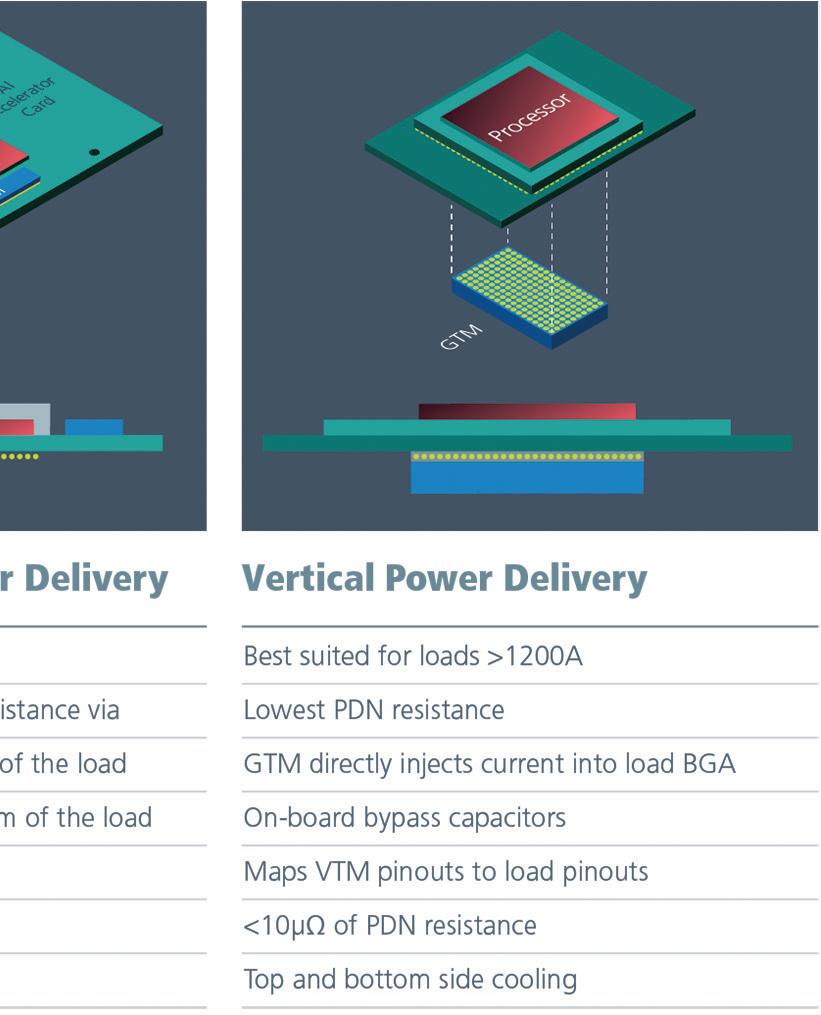
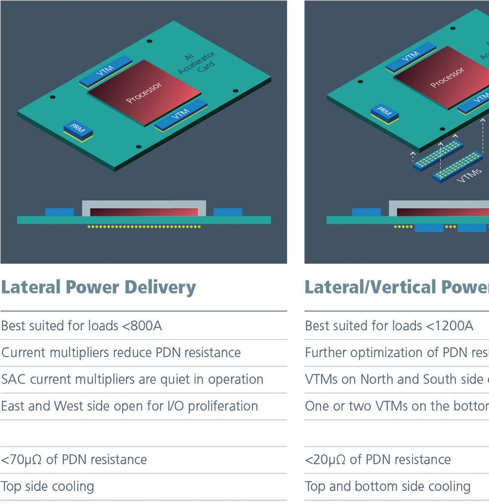

42 DESIGN WORLD — EE NETWORK 10 • 2022 eeworldonline.com | designworldonline.com POWER & ENERGY EFFICIENCY HANDBOOK

DESIGN WORLD ONLINE EVENTS AND WEBINARS Check out the DESIGN WORLD WEBINAR SERIES where manufacturers share atheir experiences and expertise to help design engineers better understand technology, product related issues and challenges. WEBINAR SERIES FOR UPCOMING AND ON-DEMAND WEBINARS, GO TO: www.designworldonline.com/design-world-online-events-and-webinars
andrea gorgerino • epc
dispelling myths: no, e g a n fets
don’t need bipolar gate drives
use of a negative gate drive can lead to a larger voltage drop during deadtime and severe losses.
g a n
devices have gone from initial R&D to mainstream designs over the last 15 years. Unfortunately there are many misunderstandings left-over from those earlystage developments or dead-end technology branches. One of the most pernicious is the topic of bipolar drive. In actuality, unipolar drives are the best way to drive eGaN FETs.
Bipolar gate drives are still used in power electronic circuits. But their applications are usually confined to high-voltage-class devices (≥ 1,200 V) and high-current circuits where layout limitations and component parameters create concerns for the cross-conduction effect called Miller effect.
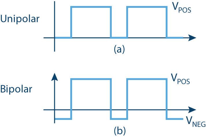
unipolar
effect of dv / dt on a device in the off-state and requirements for avoiding millerinduced shoot-through.
The Miller effect appears in halfbridge topologies and happens when the complementary device (which is OFF) is subject to a high dV/dt generated by the device in the other half of the bridge turning ON. During this event, the capacitors of the OFF device are charged by the external dV/dt.
The current of interest charges the gate-drain capacitance, also known as Miller capacitance: This current then flows either through the gate resistor and then the gate driver (which attempts to keep the device OFF), or through the gate-source capacitance. In turn, the current flowing through gatesource capacitance will create a voltage from gate to source. If this voltage exceeds the device threshold voltage, the device begins to conduct some current. This current is a
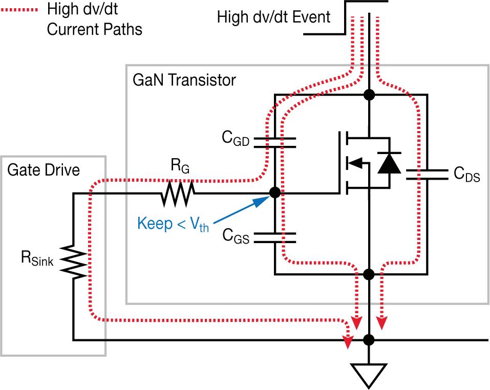
shoot-through current because it comes from the main bus capacitor and flows through both half-bridge devices. This shoot-through current leads to additional switching losses and could
on the driver. This additional OFF clamp is active after the turn-OFF event and further helps to clamp the gate during dV/dt events. But the driver must have the clamp built in. It is possible to drive the gate to a negative voltage using a bipolar gate drive. In this way the current flowing through the gate-source capacitance now must charge the gate from a negative voltage, e.g. -5 V, instead of from 0 V. This approach provides additional headroom before the threshold voltage is reached. But the technique requires generating two separate voltages for each device, so it can add significant cost and complexity to the overall design.
even lead to device failure if the voltage on the gate, and hence the current, is high enough.
Several strategies have been implemented in MOSFET designs to mitigate this effect at the circuit design level. In increasing order of complexity they are:
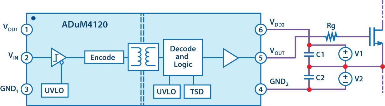
Minimizing gate loop parasitics in the layout allows the gate driver to bypass part of the current coming through the gatedrain capacitance.
Use of separate turn ON and OFF gate resistors allows the design to reduce the dV/ dt while maintaining a strong gate driver to keep the OFF device OFF. This method is most effective when combined with item one above
Finally, a driver with an active Miller clamp can be utilized. This concept can be considered an expansion of item two above, where an additional turn-OFF pin is available
c gd and q gd as a function of d-s voltage for an epc 2045 egan fet.
the miller charge ratio
Circuit-level mitigation strategies for the Miller shoot-through can add complexity and cost. Before committing to any such strategies, it is important to look at the impact of the device itself and its characteristics on this effect.
The most important parameter to consider is the Miller ratio which is defined as either a ratio of capacitances or a ratio of charges. Because semiconductor devices have quite nonlinear capacitances versus voltage, we will use the Miller charge ratio which is more accurate. It is defined as QGD/QG(TH), where QG(TH) is the pre-threshold voltage gate charge. This criterion also automatically takes into consideration the effect of different threshold voltages, as lower thresholds imply lower QGS(TH)
It should be noted that in most datasheets QGD is given at 50% of the maximum VDS of the device, while it is common to use FETs up to 80% of their rating. As an example, for an EPC2045 eGaN FET the difference in QGD from 50% to 80% voltage is about 10%.
Keeping the ratio as low as possible will minimize the voltage on the gate. More importantly, keeping the ratio below one will ensure the voltage on the gate will always stay below turn-on threshold. If this criterion
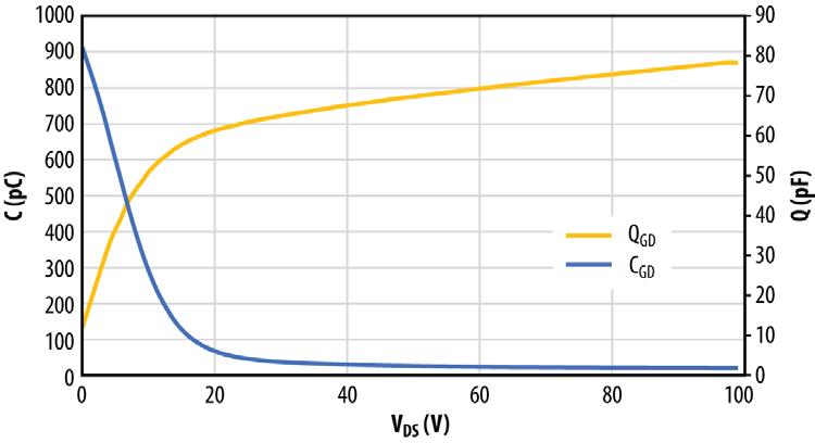
44 DESIGN WORLD — EE NETWORK 10 • 2022 eeworldonline.com | designworldonline.com
POWER & ENERGY EFFICIENCY HANDBOOK
and bipolar gate drives. an example
of a bipolar supply setup.
miller charge ratio for epc eg a n fet ( t j = 25 °c )
Qgs(th) Qgd (datasheet) Qgd/Qgs(th)
EPC2045 100 V 1.3 nC 0.8 nC 0.61
EPC2218 100 V 1.9 nC 1.5 nC 0.79
EPC2207 200 V 0.8 nC 0.7 nC 0.88
can be met, we are guaranteed to avoid any shoot through.
Miller charge ratios for EPC eGaN FETs are all below one. This means eGaN FETs are not susceptible to Miller shoot through! For comparison, many 100-V and 200-V-class silicon MOSFETs are quite susceptible to Miller shoot-through and care should be taken when using such devices.
Another important consideration is
In a silicon MOSFET, a p-n junction forms a diode from the source to the drain of the transistor. Current flowing in the reverse direction (into the source) flows through this diode. This diode has the usual characteristics of a p-n diode such as a knee voltage around 0.7 V, and forward and reverse recovery.
nominal threshold voltage variation with temperature.
comparison of reverse conduction for an epc 2045 egan fet with different vgs levels.
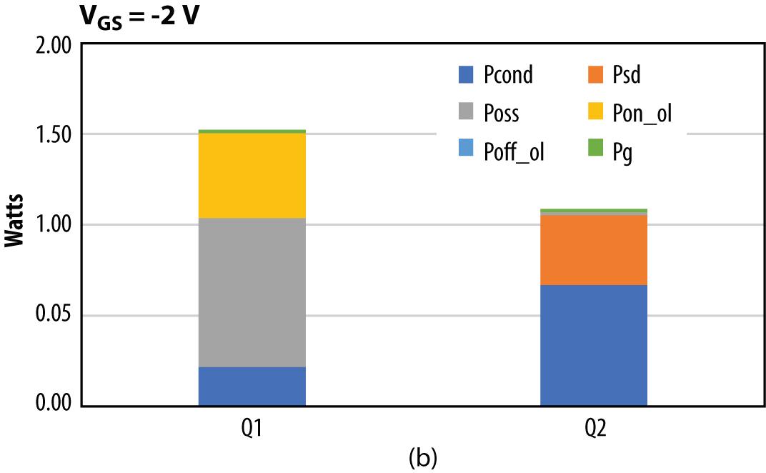
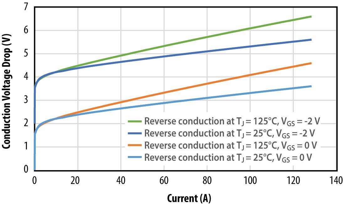
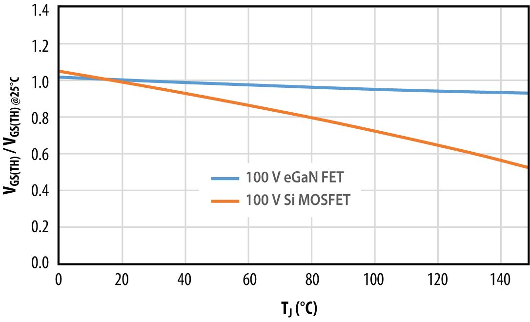
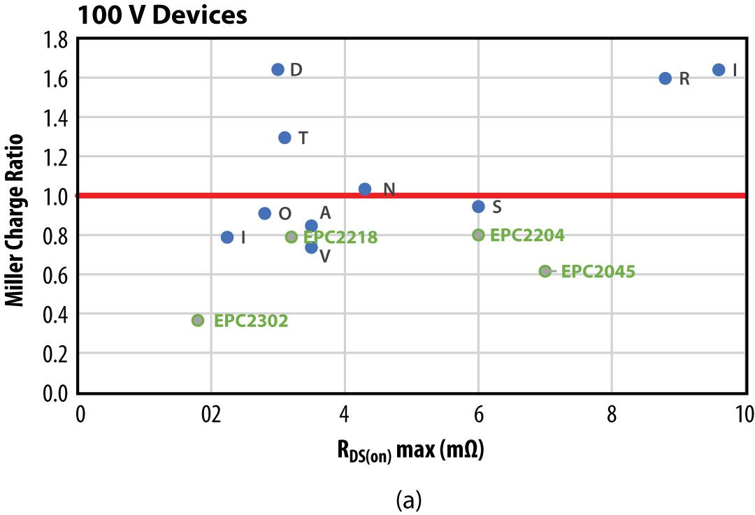
700 kHz switching frequency 48 to 12 V, 10-A output 12 nsec deadtime
Turn-OFF Vgs = 0 V or -2 V
Results graphed in the nearby figure reveal the overall losses increase by 10% from 2.4 W to 2.6 W.
We have shown why the need for bipolar gate drive for GaN FET is truly a myth. Thanks to the low Miller charge ratios always below one, the induced shoot-through will not
In contrast, a GaN FET has no such diode. This quality is an advantage because it means QRR is zero. However, GaN FETs do conduct current in the reverse direction in a way like a diode. This reverse conduction path is formed by turning on the 2DEG in the reverse direction, using the positive gate-drain voltage to enhance the channel. Therefore, if the gate voltage drops below 0 V, the reverse conduction voltage will rise by the same amount. Thus it is important not to use negative gate drive as to not increase this voltage drop.
miller charge ratios for best-in-class silicon mosfet (in blue) and gan fet (in green) 100-v devices are on the top chart, 200-v devices are on the bottom chart.
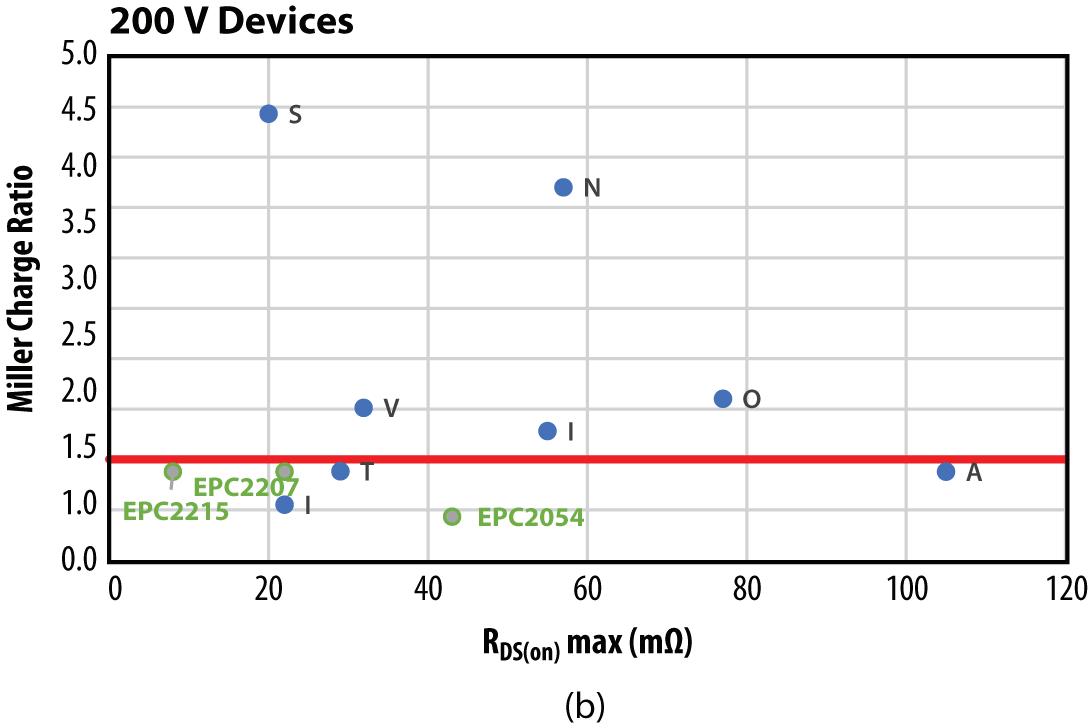
threshold voltage variation with temperature. In silicon MOSFETs the threshold voltage falls with temperature. So when the device is at its operating temperature the QG(TH) can be as much as 50% lower than the datasheet value, which means a x2 factor on the Miller charge ratio. On the other hand, the variation for any eGaN FET is less than 10%.
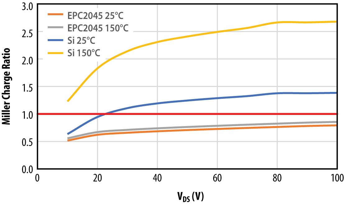
By combining these two effects (gatedrain capacitance variation with voltage and threshold voltage variation with temperature) we can also see eGaN FETs are more stable than silicon MOSFETs regardless of Miller charge ratio calculated in nominal conditions.
In a nutshell, eGaN FETs don’t need bipolar drives. More specifically, they should not be used because of reverse direction conduction in GaN FETs.
This effect is only present during the deadtime interval, as when the gate is turned ON the GaN FET will conduct current with the same on resistance as in the forward direction. Although deadtime can be reduced thanks to the fastswitching characteristics of GaN devices, the additional losses when using a negative gate drive can still add up and are best avoided.
To illustrate the more severe loss due to a negative gate drive, consider a simple synchronous buck converter during deadtime conduction. We ignore the impact of negative drive on turn-OFF losses. The main conditions for the converter are:
impact of negative gate drive on dead-time losses. turn-off v gs= 0 v on the top, v gs=- 2 v on the bottom.
happen. And use of a negative gate drive can actually lead to more severe losses because of a larger voltage drop during deadtime.
effects of vds and temperature on the miller charge ratio.
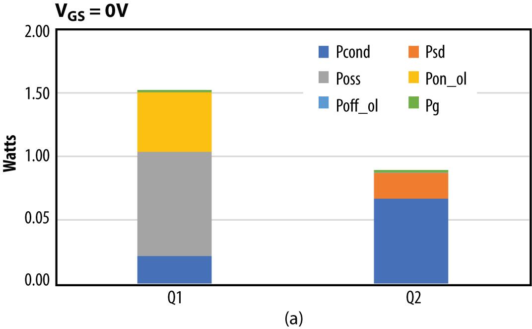
At EPC, our reference designs and demo boards are designed with unipolar gate drive (0 V turn OFF), optimized layout, and if possible, separate RgON and RgOFF. With these simple guidelines we can realize robust high performance.
references epc, www.epc-co.com
45DESIGN WORLD — EE NETWORK10 • 2022eeworldonline.com | designworldonline.com EG a N GATE DRIVES
Jami Brownlee
Jim
Mike Francesconi mfrancesconi@wtwhmedia.com
Nagle cseel@wtwhmedia.com


LEADERSHIP
Emich memich@wtwhmedia.com


Managing Director Scott McCafferty smccafferty@wtwhmedia.com
Matheson mmatheson@wtwhmedia.com 805.895.3609
AD INDEX POWER & ENERGY EFFICIENCY HANDBOOK • OCTOBER 2022 Coilcraft 11 Cornell Dubilier Electronics, Inc. ........................... 29 Digi-Key Electronics Cover, IFC Holy Stone International 35 Keystone Electronics Corp 1, IBC KOA Speer Electronics 27 Kyocera AVX ............................................................ 9 NKK Switches of America, Inc. 32 Pico Electronics ..................................................... 13 Qorvo 3 Sager Electronics 39 Sorbothane Inc. 38 Tadiran Batteries 25 Texas Instruments ................................................. BC @ designwo r l d Publisher Mike
508.446.1823 @wtwh_memich
310.279.3844 @SMMcCafferty EVP Marshall
@mmatheson SALES
jbrownlee@wtwhmedia.com 224.760.1055
Dempsey jdempsey@wtwhmedia.com 216.387.1916
630.488.9029 Courtney
440.523.1685 Jim Powers jpowers@wtwhmedia.com 312.925.7793 @jpowers_media
TEAM EE Classroom on Silicon Carbide Silicon Carbide (SiC) has made its mark in bringing faster, a smaller, and more reliable components than its fellow semiconductors to market. While SiC components have been around for a couple of decades, there is still a lot to learn and a lot to consider when choosing the most suitable WBG semiconductor for your device. LET US HELP with tutorials, from looking at how WBG semis stack up in power conversion efficiency to an overview of SiC FETs and MOSFETs. Check out our EE Classroom to learn more: www.eeworldonline.com/silicon-carbide-classroom


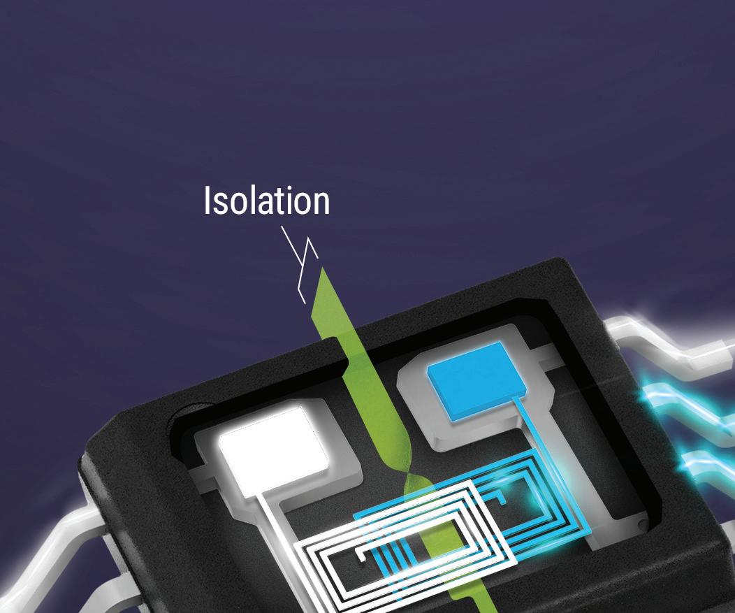


90% space savings. 50% lower cost. Industry-leading reliability. Higher system reliability with integrated isolation technology. Learn more > www.ti.com/ssr Looking for an affordable way to increase reliability of electric vehicles? Our new integrated solid-state relay portfolio of isolated switches and drivers transfers both power and signal over a single isolation barrier in a single chip, improving system safety for high-voltage automotive and industrial systems. The TPSI3050-Q1 and TPSI2140-Q1 increase reliability while reducing solution size and cost by up to 50% compared to electromechanical relays and photorelay solutions. Eliminate moving parts and switch to solid-state relays today.
