TELKOMNIKA Telecommunication Computing Electronics and Control
Vol. 21, No. 4, August 2023, pp. 909 916
ISSN: 1693-6930, DOI: 10.12928/TELKOMNIKA.v21i4.24815
Dickson voltage multiplier with 1 to 6 stages for dual-band rectifiers (2.45/5.8 GHz) with low input power
Sara El Mattar1, Abdennaceur Baghdad1 , Sara Said2,3 , Elhadi Baghaz4
1Laboratory of Electronics, Energy, Automatics and Data Processing, Department of Electrical Engineering, Faculty of Sciences and Techniques of Mohammedia, Hassan II University, Casablanca, Morocco
2Research Center, High Studies of Engineering School, EHEI, Oujda, Morocco
3Department of Physics, Faculty of Sciences, University of Mohamed Premier, Oujda, Morocco
4Laboratory of Electronics, Instrumentation and Energetic, Department of physics, Faculty of Sciences, Chouaïb Doukkali University, El Jadida, Morocco
Article Info
Article history:
Received Nov 21, 2022
Revised Dec 30, 2022
Accepted Feb 16, 2023
Keywords:
2.45 GHz/5.8 GHz
Dickson voltage multiplier
Low input range

Rectifier
RF energy harvesting
ABSTRACT
This paper presents the design of highly efficient rectifiers that can operate at WiFi frequencies (2.45 GHz and 5.8 GHz) and match low input power. The designed dual-band rectifiers use multi-stage dickson voltage multipliers (DVM) (from 1 to 6 stages), and the main idea of this paper is to find the number of stages that offers the best performance and that can be used by applications that operate within the same constraints (operating frequencies, input power). The efficiency and the output voltage (Vout) are the parameters studied to analyze the designed rectifiers. The results showed that as the number of DVM stages increased, the efficiency curves for both frequencies shifted to the higher input power range, even when using the same diode (SMS7630) and the same load (5 KΩ). We concluded that the rectifier with 1-stage DVM is the most suitable to be used for low input power at the selected frequencies since it provides an efficiency of 57.734% at 0 dBm for 2.45 GHz and 36.225% at 1 dBm of input power for 5.8 GHz.
This is an open access article under the CC BY-SA license.
Corresponding Author:
Sara El Mattar
Laboratory of Electronics, Energy, Automatics and Data Processing
Department of Electrical Engineering, Faculty of Sciences and Techniques of Mohammedia
Hassan II University, Fst Mohammedia-Casablanca, Morocco
Email: saraelmattar@gmail.com
1. INTRODUCTION
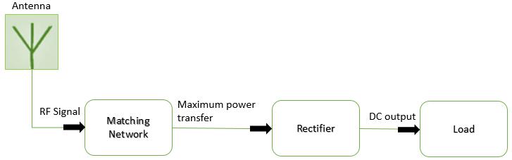
The issue of battery life has been addressed in several ways. Many researchers worldwide are focused on radio frequency (RF) energy harvesting technologies, and it is now possible to guarantee the energy independence of electronic devices. Energy harvesting (EH) is not a novel concept; in fact, Tesla introduced it more than a century ago [1]. The contactless aspect of the power transmission and the ease of deployment are only a couple of the distinctive benefits that RF harvesting has to offer (both regulated RF radiation and ambient harvesting are options for energy harvesting). Due to its widespread use, it can be deployed to power radio frequency identification (RFID) systems [2], [3], wireless sensor nodes [4], [5] and in general, any system that is powered wirelessly [6]. However, the majority of EH systems are inefficient for low-power sources, and radio frequencies are known to be a source with this limitation. This issue can be resolved by either reducing power consumption, which is constrained by physical constraints, or by using a different energy source that can provide enough power [7] The EH system generally consists of a source (antenna), whose role is to collect the RF energy present around the antenna, as well as a matching network to properly transfer the energy to the load, and a rectifier circuit, which transforms the collected RF power into useful DC power and can be a voltage multiplier or another topology. The block diagram for the RF energy harvesting system is illustrated in Figure 1.
Journal homepage: http://telkomnika.uad.ac.id
However, a significant constraint is the substantial power dissipation imposed by the physical distance of the tags from the power source, which is described using the Friis transmission model. In actuality, the amount of energy available decreases with the distance (��²), which makes powering distant tags quite challenging. The problem could be much worse since the loss in multi-path transmission could be proportional to ��4 [8]. It is obvious that high-efficiency rectifiers are required in order to turn RF EH into a practical choice given the limited quantity of energy that can be gathered. To increase efficiency and output voltages, several researchers provide a variety of architectural designs. The most often used are Dickson voltage multiplier (DVM) circuits with one or many stages based on Schottky diodes [9]–[11]
Niotaki et al. [12] present a dual-frequency rectifier for 0.915/2.45 GHz with maximum conversion efficiencies at received power levels of 0 dBm. Papadopoulou et al. [13] propose a dual-band rectifier (866 MHz and 937 MHz) with a voltage doubler topology and an input power of 0 dBm. In a similar manner, Rehman et al. [14] presents a rectifier for 2.45 GHz and 5.8 GHz; the circuit is composed of a voltage doubler, and the relevant power levels range from -30 dBm to -10 dBm, and the maximum efficiencies are obtained at 0 dBm and 1 dBm, respectively. Mattar et al. [15], a dual-band rectifier for the same operating frequencies is designed using a voltage doubler for low input power with maximum efficiency at 2 dBm for both frequencies. We have noticed from all these studies mentioned above that the most commonly used circuit in dual band designs which operate at low power ranges is a voltage doubler circuit, or as it is called in our study, a 1-stage voltage multiplier.
It is obvious that using a 1-stage DVM for design reduces the size of the rectifier, but adding additional stages often leads to improved performance. We want to answer the question of why the DVM with 1-stage is the most used circuit by rectifiers that aim for low input power and operate at multiple ranges. We propose a study of the different stages of DVM (1 to 5 stages) for 2.45 GHz and 5.8 GHz using the SMS7630 diode because this diode provides very good management for low input power. We will analyze the impacts of the number of stages for the operating frequencies in relation to the output voltage (Vout) and efficiency. According to the authors’ knowledge, this study is the only one to present an analysis of several DVM stages with dual-band features and for low input power ranges. The next sections of the article are structured as: in section 2, we will describe the different steps followed in the design of the rectifiers with 1 to 6 stages of DVM; in section 3, we will analyze the results obtained; and we will conclude this article in section 4.
2. RECTIFIER DESIGN
The purpose of a rectifier circuit is to transform electromagnetic energy into useful DC energy. It usually consists of two main parts. The first part is a matching network that modifies the impedance to create a perfect match with the rectifier diode(s). The second part is the RF to DC conversion circuit. To design a rectifier it is necessary to design all these parts and that is the role of this section.
2.1. Circuit design for RF to DC conversion
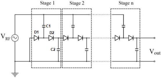
Collection transducers generally have a low power density (<10 mW/cm2) [16] which is why the voltage levels that can be reached are often lower than the operating threshold voltage of the RFID. The voltage multiplier is one of the most used structures in RF to DC conversion design because it features peak-to-peak voltage rectification from the RF signal’ full wave. For the purpose of providing a passive voltage offset, two configurations are constructed in a cascade utilizing Schottky diodes [17]. In a normal voltage multiplier rectifier, C1 and D2 create a voltage clamp, whereas D1 and C2 create a rectified peak. This structure with two diodes and two capacitors is called a voltage doubler. Thus, the output voltage is roughly double the input voltage. To attain larger DC output voltage levels, a voltage doubler can be duplicated to �� stages in a cascade and form a voltage multiplier. The overall voltage multiplier (VM) schematic design is depicted in Figure 2 Each component (stage) is made up of two diodes and two capacitors.
2.2. Impedance matching circuit
Rectifiers are non-linear circuits due to the components they use, as their input impedance varies depending on the input power, load value, and frequency. The designed circuit must resonate at the desired frequencies in order to increase circuit efficiency [18]. In order to convey the most energy from the source to the load and prevent RF signal reflection, matching networks (MN) were made to match the VM circuit’s impedance to the common 50 sources (antennas). As a result, it will enable us to obtain the greatest possible amount of converted DC power from ambient RF signals [18]–[21]
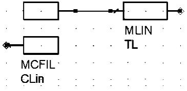
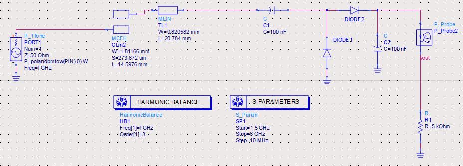
Some works [22], [23] have used MNs based on lumped components. When the frequency is higher than 1 GHz, these components exhibit increased noise and therefore greater loss. As a result, microstrip lines are increasingly being used in circuits operating at 2.45 GHz and 5.8 GHz [24], [25]. The matching unit of our circuit is designed with microstrip lines. Rogers RT/Duroid 5880, having a thickness of 1575 mm, was selected as the substrate for our circuit. We determine the rectifier’s input impedance using the S-parameter simulation in the ADS software. The MN’s initial design parameters are then determined using MATLAB and the design equations shown in [26]. Then, using the advanced design system (ADS) tool for optimization, we adjusted the result parameters to match the input impedance for a load of 5 KΩ and for low input power in the appropriate frequency bands. By using a matching network with a DC-blocking feature, the voltage doubler’s input DC block capacitor (C1) is removed. These mentioned steps will be repeated to design each number of DVM stages. Figure 3 illustrates the used MN circuit, comprising both a transmission line (TL) and a coupled transmission line referred to as (Clin). Table 1 describes the values of the matching network parameters for each number of stages, where (W) represents the width, (L) denotes the physical length, and (S) signifies the separation between the transmission line conductors.
2.3. DVM rectifier power losses sources
Substrate loss, diode loss, and impedance mismatch loss, all affect a rectifier’s conversion efficiency While diode loss represents the most significant loss of these losses. Two distinct factors account for the changes in diode efficiency for each input power region On the one hand, the loss due to the integrated potential of the forward diode (threshold voltage) at low input power. On the other hand, the loss related to the breakdown voltage of the diode at high input power.
2.3.1. In the region of low input power
The reverse peak voltage is lower than the breakdown voltage on the diode while the input voltage is low. Diode losses in this region are produced by the overlapping voltage and current at the diode junction and at the series resistance (����) because the voltage over the junction capacitance (����) changes considerably. According to [27] the multi-stage DVM power losses at the diode junction and for the region of low input power can be defined using (1) where the number of stages is (��), (����) and (����) represent the maximum magnitude of the current and the diode voltage, (����ℎ) is the built-in potential and (��) is the operating frequency of the rectifier.
2.3.2. In high input power region
The current circulates in the direct direction in a diode. In the other direction, there is no current. On the other hand, if the reverse voltage is steadily increased, a current may abruptly start to flow at any time. The breakdown voltage (������) is the value at this point. Due to the high-power loss during the breakdown phase, the diode performance starts to decrease. When a voltage greater than the breakdown voltage is applied to the diode, leakage current will start flowing in the opposite direction, and this is what mostly degrades the diode characteristics. The (2) [28] may be used to determine the power loss of multi-stage DVM in high input power. Where (����) is the reverse current, and (��) represents the proportion of the rise and fall time in relation to the half-period.
The diodes must have the lowest threshold voltage and the fastest switching possible because of the high frequencies used and the low input signal [29]. Among the different varieties of Schottky diodes, we decided to choose SMS7630 in our circuits since it has a low threshold voltage and was created and tuned for usage in low input signal applications [30], [31] An online datasheet was used to get the SPICE model of the Schottky SMS7630 diode for the simulations.
3. RESULTS AND DISCUSSION
By using the elements described in the previous sections, the Dickson voltage multiplier circuit was designed and improved. The ADS 2019 software, with the use of the harmonic balance for the calculation of output voltage and rectifier efficiency. The S-parameter simulator technique was used to calculate the S11 coefficient of the rectifiers. Then the motion technique will be used for this section to build and simulate the DVM circuit.
3.1. Circuit impedance matching
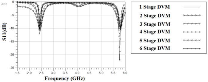
Since the source (antenna) is directly connected to the DVM circuit through impedance matching, we constructed a multistage DVM with matching circuits suitable for each number of DVM stages and computed the Vout and efficiency of each resulting circuit (IMN+DVM). Figure 4 shows the schematic for the ADS circuit rectifier, consisting of a matching circuit, a 1-stage DVM, and a load of 5 KΩ. Using a 5 KΩ load with an input power of -10 dBm, Figure 5 shows the simulated rectifiers’ S11 parameter. As can be seen, the rectifiers are well-matched at the required frequencies. Normally, when the S11 is smaller than -8 dB, the circuit resonates in our case with all rectifiers having an S11 value ≤ -10 dB.
3.2. Rectifiers efficiency
The ratio of the output DC power (Pout) to the input RF power (PIN) is one of the most important performance metrics that can be used to determine how efficiently RF power is converted to DC power. The efficiency of a rectifier can be calculated using the following (3)
�������������������� =100× ������������ ������ (3)
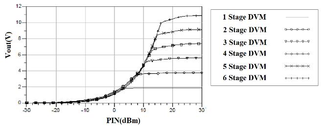
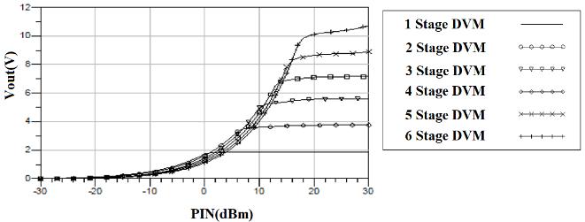
Where ������������ represents the resulting continuous power of the rectifier and PIN is the input power. Simulations with a range of stage numbers from 1 to 6, and sweep input power values between -30 dBm and 30 dBm were employed. Figure 6 and Figure 7 illustrate how the number of stages in VM circuit design affects efficiency and output power of a dual band (2.45/5.8 GHz) rectifier respectively.
The efficiency variation gradually disappears, as shown in Figure 6(a) and Figure 6(b). Table 2 shows the maximum efficiencies for each DVM and details the efficiencies achieved by the DVMs for different PIN ranges. The efficiency curves for both frequencies move toward the higher input power range as the DVM stage number rises. This can be explained by the fact that there will be more power losses in the low-input power region. For 2.45 GHz, and especially for low input power (PIN ≤ 0 dBm) at 5.8 GHz, the efficiency of the one-stage rectifier is significantly higher than that of the other voltage multiplier upper stages circuits.
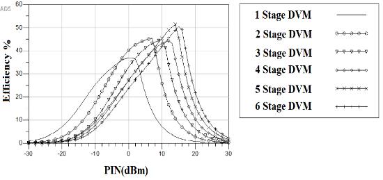
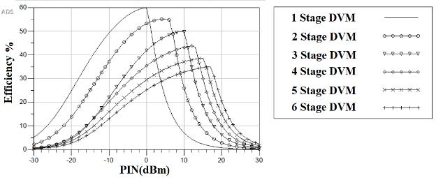
We can see in Figure 6 that as the number of stages increases, the efficiency at low input power decreases (PIN ≤ 0 dBm) and increases for the highest input power (PIN > 0 dBm). For example, the single-stage rectifier achieves a maximum of 59.76% and 36.75% at 0 dBm at 2.45 GHz and 5.8 GHz, respectively, while the 6-stage rectifier achieves its peak of 34.95% and 50.429% at high input powers of 15 dBm and 17 dBm, respectively. While using the low input power levels at the rectifiers, their efficiency degraded for both frequencies. This degradation in the rectifiers’ performances with the addition of additional stages can be explained by the losses related to the number of diodes employed as well as the losses linked to the used substrate. As illustrated in Figure 7, there are no discernible differences between the various DVM stages circuits for low input powers (PIN < 0 dBm), but for input values greater than 10 dBm, increasing the stage number results in higher output voltage, and this is true for both operating frequencies as shown in Figure 7(a) and Figure 7(b).
(a)
(b)
Figure 7. Simulation results of output DC voltage as a function of input power and number of DVM stages for (a) 2.45 GHz and (b) 5.8 GHz
3.3. Theoretical explanation of the results
A single-diode rectifier will perform better than a multi-diode rectifier at a low input power level. This is due to the extra losses in rectifier circuits with multi-stages described in (1), particularly the series loss from ����, whose sum increases with rising �� (and also current), and the loss related to the RC filter, as the low-pass cutoff frequency drops with increasing ��. More losses will result from a rectifier with more stages since the load must pass through each diode. This is true for the two operating frequencies, but for the 5.8 GHz frequency, in addition to the losses mentioned, there is a production of losses linked to the increase in frequency.
For rectifiers with more stages, the reached DC output voltage is higher because the rectifier as a whole has a higher breakdown voltage in relation to the output. It is also clear that the number of stages increases the input power at which the rectifier output voltage reaches its maximum. The increasing loss related to each diode in the rectifier circuit is the source of this phenomenon. As a result, more input power is required to achieve the same outcome and overcome the produced losses. In summary, high numbers of stages are mostly advantageous at high powers since they enable the rectification of greater quantities of power. Conversely, at low input powers, a smaller number of diodes are advantageous since this will produce fewer loss factors.
4. CONCLUSION
We carried out this study in order to create dual-band rectifiers that function at 2.45 GHz and 5.8 GHz precisely and with low input power densities. The design employed a Dickson voltage multiplier topology with stages ranging from 1 stage to 6 stages, the same diode type SMS7630, the same load value of 5 KΩ, and an impedance matching circuit for each stage’s number. The goal of these designs is to find the best stage number of DVM for use in rectifiers with dual band (2.45/5.8 GHz) and low power densities. The results obtained showed that the more stages are added, the more the DC voltage increases, but this increase is only true for an input power of more than 0 dBm because the voltages produced at low power levels are almost the same for all DVM stage numbers. Regarding rectifier efficiency for both frequencies, it shifts to the higher input power range as the number of DVM stages increases. Based on theoretical study and performance comparison, our analsys has shown that for dual band operation and exactly at 2.45/5.8 GHz, the most efficient energy harvester for low input power levels will have the fewest stages. Above a relatively low power level, more stages will be needed to provide the maximum DC output voltage. Above a certain input level, additional stages will result in a higher voltage.
REFERENCES
[1] A. S. Marincic, “Nikola Tesla and the wireless transmission of energy,” IEEE Transactions on Power Apparatus and Systems, vol. PAS-101, no. 10, pp. 4064–4068, 1982, doi: 10.1109/TPAS.1982.317084.
[2] M. T. Bevacqua, G. G. Bellizzi, and M. Merenda, “Field focusing for energy harvesting applications in smart RFID tag,” in 2019 IEEE International Conferenceon RFIDTechnologyand Applications(RFID-TA),2019, pp.263-266,doi:10.1109/RFID-TA.2019.8892014.
[3] W. A. Indra, A. W Y Khang, Y. T. Yung, J. Abedalrahim, and J. Alsayaydeh, “Radio-frequency identification (RFID) item finder using radio frequency energy harvesting,” ARPN Journal of Engineering and Applied Sciences, vol. 14, no. 20, pp. 3554–3560, 2019. [Online]. Available: http://www.arpnjournals.org/jeas/research_papers/rp_2019/jeas_1019_7964.pdf
[4] H. Zhang, Y. -X. Guo, Z. Zhong, and W. Wu, “Cooperative integration of RF energy harvesting and dedicated WPT for wireless sensor networks,” IEEEMicrowaveand WirelessComponentsLetters,vol.29,no.4,pp.291–293,2019,doi:10.1109/LMWC.2019.2902047.
[5] M. Sansoy, A. S. Buttar, and R. Goyal, “Empowering wireless sensor networks with RF energy harvesting,” in 2020 7th International Conference on Signal Processing and Integrated Networks (SPIN), 2020, pp. 273-277, doi: 10.1109/SPIN48934.2020.9071376.
[6] T. Khan, Nasimuddin, and Y. M. M. Antar, Elements of Radio Frequency Energy Harvesting and Wireless Power Transfer Systems Boca Raton, FL, USA: CRC Press, 2020, doi: 10.1201/9780429283918
[7] M. M. Ababneh, S. Perez, and S. Thomas, “Optimized power management circuit for RF energy harvesting system,” in 2017 IEEE 18th Wireless and Microwave Technology Conference (WAMICON), 2017, pp. 1-4, doi: 10.1109/WAMICON.2017.7930238.
[8] P. V. Nikitin and K. V. S. Rao, “Antennas and Propagation in UHF RFID Systems,” in 2008 IEEE International Conference on RFID, 2008, pp. 277-288, doi: 10.1109/RFID.2008.4519368.
[9] A. Ballo, A. D. Grasso, and G. Palumbo, “A review of charge pump topologies for the power management of IoT nodes,” Electronics, vol. 8, no. 5, 2019, doi: 10.3390/electronics8050480.
[10] A. Jaiwanglok, K. Eguchi, A. Julsereewong, and P. Pannil, “Alternative of high voltage multipliers utilizing Cockcroft–Walton multiplier blocks for 220 V and 50 Hz input,” Energy Reports, vol. 6, pp. 909–913, 2020, doi: 10.1016/j.egyr.2020.11.110.
[11] I. Chaour, A. Fakhfakh, and O. Kanoun, “Enhanced passive RF-DC converter circuit efficiency for low RF energy harvesting,” Sensors, vol. 17, no. 3, 2017, doi: 10.3390/s17030546.
[12] K. Niotaki, S. Kim, S. Jeong, A. Collado, A. Georgiadis, and M. M. Tentzeris, “A compact dual-band rectenna using slot-loaded dual band folded dipole antenna,” IEEE Antennas and Wireless Propagation Letters, vol. 12, pp. 1634–1637, 2013, doi: 10.1109/LAWP.2013.2294200.
[13] M. S. Papadopoulou et al., “Dual-band RF-to-DC rectifier with high efficiency for RF energy harvesting applications,” in 2020 9th International Conference on Modern Circuits and Systems Technologies (MOCAST), 2020, pp. 1-4, doi: 10.1109/MOCAST49295.2020.9200262.
[14] M. U. Rehman, W. Ahmad, and W. T. Khan, “Highly efficient dualband 2.45/5.85 GHz rectifier for RF energyharvesting applications in ISM band,”in 2017 IEEEAsia PacificMicrowaveConference(APMC),2017,pp.150-153,doi:10.1109/APMC.2017.8251400.
[15] S. E. Mattar, A. Baghdad, and A. Ballouk, “A 2.45/5.8 GHz high-efficiency dual-band rectifier for low radio frequency input power,” International Journal of Electrical and Computer Engineering (IJECE), vol. 12, no. 3, pp. 2169-2176, 2022, doi: 10.11591/ijece.v12i3.pp2169-2176.
[16] L. -G. Tran, H. -K. Cha, and W. -T. Park, “RF power harvesting: a review on designing methodologies and applications,” Micro and Nano Systems Letters, vol. 5, no. 14, 2017, doi: 10.1186/s40486-017-0051-0.
[17] C. H. P. Lorenz, S. Hemour, and K. Wu, “Physical mechanism and theoretical foundation of ambient RF power harvesting using zero-bias diodes,” IEEE Transactions on Microwave Theory and Techniques, vol. 64, no. 7, pp. 2146–2158, 2016, doi: 10.1109/TMTT.2016.2574848.
[18] G. Monti, L. Tarricone, and M. Spartano, “X-Band planar rectenna,” IEEE Antennas and Wireless Propagation Letters, vol. 10, pp. 1116–1119, 2011, doi: 10.1109/LAWP.2011.2171029.
[19] X. -X. Yang, C. Jiang, A. Z. Elsherbeni, F. Yang, and Y. -Q. Wang, “A novel compact printed rectenna for data communication systems,” IEEE Transactions on Antennas and Propagation, vol. 61, no. 5, pp. 2532–2539, 2013, doi: 10.1109/TAP.2013.2244550.
[20] Y. -Y. Gao, X. Yang, C. Jiang, and J. -Y. Zhou, “A circularly polarized rectenna with low profile for wireless power transmission,” Progress in Electromagnetics Research Letters, vol. 13, pp. 41–49, 2010, doi: 10.2528/PIERL09111805.
[21] P. Kim, G. Chaudhary, and Y. Jeong, “A dual-band rf energy harvesting using frequency limited dual-band impedance matching,” Progress In Electromagnetics Research, vol. 141, pp. 443–461, 2013, doi: 10.2528/PIER13061704.
[22] A. Nimo, D. Grgić, and L. M. Reindl, “Optimization of passive low power wireless electromagnetic energy harvesters,” Sensors, vol. 12, no. 10, pp. 13636-13663, 2012, doi: 10.3390/s121013636.
[23] K. Suri, M. Mohta, A. Rajawat, and S. H. Gupta, “A 5.8 GHz inset-fed rectenna for RF energy harvesting applications,” in 2017 International Conference on Intelligent Communication and Computational Techniques (ICCT), 2017, pp. 32-35, doi: 10.1109/INTELCCT.2017.8324016.
[24] S. E Mattar, A. Baghdad, and A. Ballouk, “A novel two-branch dual-band rectifier for 2.45 GHz 5.8 GHz RFID systems,” in WITS 2020, 2020, pp. 943–948, doi: 10.1007/978-981-33-6893-4_85.
[25] M. S. Papadopoulou, A. D. Boursianis, A. Chatzopoulos, P. Sarigiannidis, S. Nikolaidis, and S. K. Goudos, “Comparative Performance of Algorithmic Techniques for Optimizing Dual-Band Rectifier,” in 2022 11th International Conference on Modern Circuits and Systems Technologies (MOCAST), 2022, pp. 1-4, doi: 10.1109/MOCAST54814.2022.9837645.
[26] E. Khansalee, K. Nuanyai, and Y. Zhao, “A Dual-Band Rectifier for RF Energy Harvesting,” Engineering Journal, vol. 19, no. 5, pp. 189
197, 2015. [Online]. Available: https://www.engj.org/index.php/ej/article/view/908
[27] Y. Wu, Y. Liu, S. Li, and C. Yu, “New coupled-line dual-band dc-block transformer for arbitrary complex frequency-dependent load impedance,” Microwave and Optical Technology Letters, vol. 54, no. 1, pp. 139–142, 2012, doi: 10.1002/mop.26480.
[28] J. Kim, I. Park, and H. Ku, “Design of a highly efficient n-stage harmonic terminated voltage multiplier for wireless power transfer,” Energies, vol. 14, no. 21, 2021, doi: 10.3390/en14217203.
[29] C. Merz, G. Kupris, and M. Niedernhuber, “A low power design for radio frequency energy harvesting applications,” in 2014 2nd International Symposium on Wireless Systems within the Conferences on Intelligent Data Acquisition and Advanced Computing Systems, 2014, pp. 74-78, doi: 10.1109/IDAACS-SWS.2014.6954627.
[30] S. E Mattar, A. Baghdad, and A. Ballouk, “5.8 GHz Rectenna Using Dielectric Resonator Antenna,” in 2019 7th Mediterranean Congress of Telecommunications (CMT), 2019, pp. 1-5, doi: 10.1109/CMT.2019.8931317
[31] H. P. Paz, V. S. Silva, E. V. V. Cambero, H. X. Araújo, I. R. S. Casella, and C. E. Capovilla, “A survey on low power RF rectifiers efficiency for low cost energy harvesting applications,” AEU - International Journal of Electronics and Communications, vol. 112, 2019, doi: 10.1016/j.aeue.2019.152963.
Dickson voltage multiplier with 1 to 6 stages for dual-band rectifiers (2.45/5.8 GHz) with … (Sara El Mattar)
ISSN: 1693-6930
BIOGRAPHIES OF AUTHORS
Sara El Mattar born in Mohammedia Morocco on October 14, 1995. In 2016, she obtained her license degree in telecommunications engineering at the Faculty of Science and Technology of Mohammedia, then she had got a master’s degree in Internet of Things and Mobile Systems at national school of applied sciences in Fez. She is currently a Ph.D. student in the Laboratory of Electronics, Energy, Automatics and Data Processing (EEA&TI) at the Faculty of Science and Technology of Mohammedia - Hassan II University Casablanca. Her works studies are focused on the design and the optimization of the passive RFID tags and especially energy harvesting technology, with the direction of Pr. A. Baghdad. She can be contacted at email: saraelmattar@gmail.com

Abdennaceur Baghdad holds in 1992 a Ph.D. in Electronics from the University of Lille-France. He is a professor of electronics, Hyperfrequencies, antennas, and telecommunication at the University Hassan II Mohammedia Casablanca- Morocco. He is a member of the EEA&TI laboratory (electronics, energy, automatic, and information processing). His research interests are in the fields of information and telecommunication technologies. He can be contacted at email: nasser_baghdad@yahoo.fr.
Sara Said was born in Oujda, Morocco in 1992. She received the bachelor and the master degrees in electronics and informatics from University Mohamed Premier of Oujda (Morocco) in 2013 and 2015 respectively. She is now pursuing her Ph.D. degree at the Faculty of Sciences of Oujda. He interest is designing new antenna topologies based on EBG materials. She can be contacted at email: said.sara63@gmail.com

Elhadi Baghaz was born in Al Hoceima City (Morocco) in 1985. Professor researcher at the Laboratory of Electronics, Instrumentation and Energetics at the Faculty of Science of El jadida, University Chouaïb Doukkali. He can be contacted at email: e.baghaz@yahoo.fr