Vector Analysis of Electrical Networks for Temperature Measurement of MOS Power Transistors
of the tested device. The electrical conditions for these measurements were: VGS = 0 V(OFF)/10 V(ON) and VDS = 20 V. The collected data was analyzed in order to estimate changes in the values of selected parameters as the function of the ambient temperature THEAT and TMOS. Before the measurements, a simple simulation of the transistor’s operation was carried out at the ambient temperature Ta = 25 °C using the LTspice XVII program. The schematic diagram of the modeled circuit is shown in Fig. 4. In order to make the model compatible with the experiment, the series inductance L1 was added to the gate connection (Fig. 4). It corresponds to the inductance of the wire several cm long used in the experiment. Switching the transistor was achieved by changing the value of the resistance R1 from a few MΩ to 10 kΩ. Voltage source V2 simulates the VNA generator. Changing the frequency of this generator allows to estimate the impedance character of the measured device. Due to the LC series branch, at lower frequency values the impedance between gate and ground starts from capacitive to resonance at frequency around 10 MHz. For higher frequencies, the input circuit becomes inductive. This simulation result is in line with the experimental result obtained by the VNA.
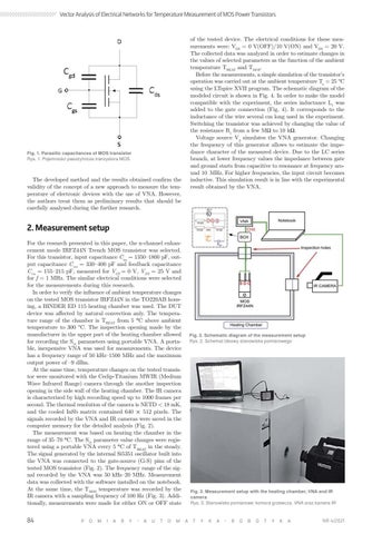
Fig. 1. Parasitic capacitances of MOS transistor Rys. 1. Pojemności pasożytnicze tranzystora MOS
The developed method and the results obtained confirm the validity of the concept of a new approach to measure the temperature of electronic devices with the use of VNA. However, the authors treat them as preliminary results that should be carefully analysed during the further research.
L6 ! For the research presented in this paper, the n-channel enhancement mode IRFZ44N Trench MOS transistor was selected. For this transistor, input capacitance Ciss = 1350–1800 pF, output capacitance Coss = 330–400 pF and feedback capacitance Crss = 155–215 pF, measured for VGS = 0 V, VDS = 25 V and for f = 1 MHz. The similar electrical conditions were selected for the measurements during this research. In order to verify the influence of ambient temperature changes on the tested MOS transistor IRFZ44N in the TO220AB housing, a BINDER ED 115 heating chamber was used. The DUT device was affected by natural convection anly. The temperature range of the chamber is THEAT from 5 °C above ambient temperature to 300 °C. The inspection opening made by the manufacturer in the upper part of the heating chamber allowed for recording the S11 parameters using portable VNA. A portable, inexpensive VNA was used for measurements. The device has a frequency range of 50 kHz–1500 MHz and the maximum output power of –9 dBm. At the same time, temperature changes on the tested transistor were monitored with the Cedip-Titanium MWIR (Medium Wave Infrared Range) camera through the another inspection opening in the side wall of the heating chamber. The IR camera is characterized by high recording speed up to 1000 frames per second. The thermal resolution of the camera is NETD < 18 mK, and the cooled InSb matrix contained 640 × 512 pixels. The signals recorded by the VNA and IR cameras were saved in the computer memory for the detailed analysis (Fig. 2). The measurement was based on heating the chamber in the range of 35–70 °C. The S11 parameter value changes were registered using a portable VNA every 5 °C of THEAT in the steady. The signal generated by the internal Si5351 oscillator built into the VNA was connected to the gate-source (G-S) pins of the tested MOS transistor (Fig. 2). The frequency range of the signal recorded by the VNA was 50 kHz–20 MHz. Measurement data was collected with the software installed on the notebook. At the same time, the TMOS temperature was recorded by the IR camera with a sampling frequency of 100 Hz (Fig. 3). Additionally, measurements were made for either ON or OFF state
84
P
O
M
I
A
R
Y
•
A
U
T
O
M
Fig. 2. Schematic diagram of the measurement setup Rys. 2. Schemat ideowy stanowiska pomiarowego
Fig. 3. Measurement setup with the heating chamber, VNA and IR camera Rys. 3. Stanowisko pomiarowe: komora grzewcza, VNA oraz kamera IR
A
T
Y
K
A
•
R
O
B
O
T
Y
K
A
N R 4 /2021