Scope of Document
This white paper highlights some of the features of DDR5 DRAM-based DIMMs (DDR5 DIMMs). System designers and others who are involved in the evaluation of next-gen memory solutions for their applications and products can use the information to determine the suitability of DDR5 DIMMs to migrate from their DDR4-based memory solutions or for new memory sub-system designs in applications requiring the additional Reliability, Availability, and Serviceability (RAS) of DDR5 memory.
DDR5 Introduction
DDR5 DRAM products provide low-latency, high-performance, almost infinite access endurance and low-power consumption, which makes them suitable for applications requiring complex system deployments to hand-held devices.
DDR5 memory devices support data rates at a lower I/O Voltage than DDR4. DDR5 DRAMs and dual-inline memory modules (DIMMs) based on DDR5 DRAMs are industry-standard products driven by the Joint Electron Device Engineering Council, or JEDEC.
SMART Modular Technologies is a contributing member to JEDEC, and worked closely with other members to define the standards for DDR5 memory devices, including DIMMs.
DDR5 Features and Applications
DDR5 features data rates of up to 6400 MT/s at 1.1V I/O voltage, addressing the needs of several applications, such as:
• Networking
• Cloud Computing
• PCs and Servers
• Embedded Computing
DIMMs are built using x4-, x8- or x16 DRAMs which can cater to applications that typically have different priorities. Some compute-intensive applications can implement their memory sub-system using x80 DIMMs, based on more cost-effective x8- or x16 DRAMs. Such applications can also leverage the higher Reliability, Availability, and Serviceability (RAS) features of DDR5based DIMMS to minimize the downtime during memory-related failures.
DDR5 DIMMs are a natural progression from DDR4 DIMMs or earlier iterations, and provide system designers with an easy path to upgrade their product offerings. DDR5 DIMMs at 4800 MT/s (DDR5 4800) are planned for release followed by higher speed grades (DDR5 5600, DDR5 6400).
DDR5 DIMMs support burst lengths of 16 beats, better refresh/pre-charge schemes allowing higher performance, a dualchannel DIMM architecture offering better channel utilization, integrated voltage regulators, increased bank-group for higher performance, and Command/Address on-die termination (ODT), a few of the many new DDR5 features enabling higher performance.
DDR5 vs. DDR4 DIMMS
Defined by the industry to increase memory bandwidth to address the need for CPU cores to have access to more memory bandwidth per core, DDR5 has intentionally increased latency over DDR4 in favor of increasing bandwidth. Applications that require low latency but do not need the increased bandwidth of DDR5 may benefit by remaining with DDR4 DRAM technology.
Besides increased memory bandwidth, DDR5 also introduces several RAS features to ensure channel robustness at increased speeds. Some of these features resulting in higher DDR5 channel robustness include duty cycle adjuster (DCA), on-die ECC, DRAM receive I/O equalization, Cyclic Redundancy Check (CRC) for both RD and WR data, and internal DQS delay monitoring.
Table 1 provides a high-level comparison of features of DDR4 and DDR5 DIMMs.
Table 1: DDR5 vs. DDR4 DIMMs
Post Package Repair
Multiple target rows per back up One target row backup per bank
Page Size 512 B or 1 kB 1 kB or 2 kB
PMIC On Mother board On-DIMM
Temperature Sensor Integrated with SPD EEPROM One on each end of DIMM
IO Voltage 1.2 V 1.1 V
Channel Architecture
Single channel Dual channel
Sub-channels None Two, independent
Gb vs 64 Gb devices
Improved backup time for “soft” repairs of deployed memory
Improved page size
Improved power management
Improved reliability
Lower power
Lower latency – better signal integrity, individual clock signals.
Increased memory density, system bandwidth and performance.
ECC 72-bit (64 data + 8 ECC) 40-bit (32 data + 8 ECC) Improved protection from single-bit errors
Burst Length 8 16
1DDR5 DIMM enhancements driven primarily by DDR5 memory devices.
Higher memory efficiency
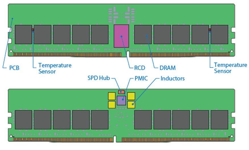
The on-DIMM power management IC (PMIC) allows for better power efficiency and frees up host cycles and real estate on the system controller motherboard. The PMIC performs voltage regulation, configuration of voltage ramps, managing voltage levels and current monitoring on the DDR5 DIMM reducing the scope and complexity of the DRAM power delivery network (PDN) management on the motherboard.
The temperature sensors enable thermal management of the memory system for smooth performance degradation or shutdown using industry-standard, operational frequency-reduction techniques called temperature throttling. Both RDIMMs and LRDIMMs have two integrated circuit temperature sensors located strategically at each end of the DIMM between the memory components.
Most other enhancements are from the DDR5 memory devices. Table 2 provides a high-level features-comparison of DDR4 and DDR5 DRAMs.
DDR5 vs. DDR4 DRAM
DDR5 is the next evolution in DRAM, bringing a robust list of new features geared to increase reliability, availability, and serviceability (RAS) by reducing power and dramatically improving performance.
Table 2 provides a high-level comparison of features of DDR4 and DDR5 DRAM.
Table 2: DDR5 vs. DDR4 DRAM
Feature
Data
Prefetch
DQ receiver equalization
Duty cycle adjustment (DCA)
Internal DQS delay monitoring
On die ECC
CRC Read
Command/address interface
ODT
One cycle: ODT, CKE, ACT, RAS, CAS, WE, A<X:0>
DQS and DQ
DQS interval oscillator
128-bit+8-bit SEC error check and scrub
Read/Write
Two cycles for some commands CA<13:0>
DQ, DQS, DM/DBI DQ, DQS, DM, CA bus
Burst length 8 (and 4) 16 and 32 (and BC8 OTF, BL32 OTF)
MIR (“mirror” pin)
Bus inversion
Data bus inversion (DBI)
Available
Command/address inversion (CAI)
CA training, CS training Yes
Write leveling training modes Yes
Read training patterns
Mode registers
Possible with the MPR
7 x 17 bits
PRECHARGE commands All bank and per bank
REFRESH commands All bank
Loopback mode
Improved
Dedicated MRs for serial (user defined), clock and LFSR -generated training patterns
Up to 256 x 8 bits (LPDDR type read/write)
All bank, per bank, and same bank
All bank and same bank
None Yes
Improved voltage margins and BOM costs
Lowered internal core clock
Improved DQ data eyes
Improved signal reliability
Improved reliability
Improved protection from bit errors
Improved reliability
Simplified interface by reducing the CA pin count
Improved signal integrity and BOM costs
64B cache-line fetch enabled with 1 DIMM sub-channel
Improved DIMM signaling
Improved reliability, accessibility through reduced VDDQ noise
Improved timing margin on CA and CS pins
Compensates for unmatched DQ-DQS path
Makes read timing margin more robust
Provides room to expand
PREsb enables precharging-specific bank in each BG
REFsb enables refreshing of specific bank in each BG
Enables testing of the DQ and DQS signaling
DDR5 Enhancements
Dual channel Architecture Implementation
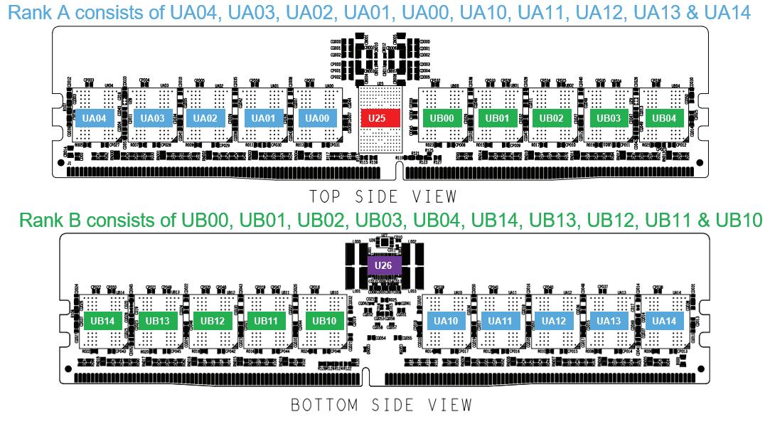
In addition to the presence of two, independent channels on the DDR5 DIMM, each DRAM device allows configuration in a primary/secondary topology, enabling logical ranks for increased density.
• DDR5 DIMMs have two channels, each 40-bits wide (32 data and 8 ECC). DDR4 DIMMs have a single 72-bit bus (64 data and 8 ECC). For the same data width (64-bits), having two smaller independent channels improves memory access efficiency.
• Independent 40-bit wide channels share the RCD that serves each of the left and right side of the DIMM.
• An independent clock for each lane improves signal integrity by increasing the noise margin.
Rank(s) Left Side A
Rank(s) Left Side B
40 Bits Independent Channel A 40 Bits Independent Channel B
Duty Cycle Adjuster (DCA)
The host uses this feature to compensate for duty cycle distortion on all DQS and DQ pins for each device enhancing the accuracy of the Read data.
On-die ECC
DDR5 DRAM allows implementation of 8-bit ECC storage for every 128 bits of data to protect the memory array against single-bit errors.
• On-die ECC is an advanced RAS feature that the DDR5 system can enable for higher speeds.
• The DRAMs internally compute the ECC for the WR data and store the ECC code in the additional storage.
• On a read operation, the DRAMs read out both the actual data as well as the ECC code and can correct any single-bit error on any of the read data bits.
• On-die ECC provides further protection against single-bit errors inside the DDR5 memory arrays.
• As this scheme does not offer any protection against errors occurring on the DDR channel, on-die ECC is used in conjunction with side-band ECC for enhanced end-to-end RAS on memory subsystems.
The following figure shows write and read operation flows with on-die ECC.
WR and RD operation flows with On-die ECC in the figure below.
WRITE operation
DRAM Receive DQ Equalization
READ operation
DDR5 DRAM support equalization for Write data by opening the WR DQ eye at the DRAM end. The improved margins protect the channel from inter-symbol interference (ISI) and enable higher data rates.
Cyclic Redundancy Check (CRC) for RD data
Extending CRC to RD data provides protection against read errors that could potentially occur in the channel.
DQS Delay Monitoring
DDR5 DRAM can monitor DQS delays and report changes due to voltage and temperature variations to the host. The information is useful for recalibrating the channel periodically by the host to maintain memory system performance.
Mode Registers
DDR5 DRAM mode registers store and provide information to the host for changing some performance characteristics on an as-needed basis for optimal system performance.
Post Package Repair Enhancements
Post package Repair (PPR) is broken into two separate repair features, hPPR (hard) and sPPR (soft) which maybe better described as permanent repair (hPPR) and temporary repair (sPPR). hPPR is non-volatile with power cycling whereas sPPR is not.
The DDR4 SDRAM has several rows per bank where are to be backed up prior to an sPPR event. A key DDR5 enhancement is the reduction of rows that need to be backed up before performing an sPPR repair. DDR5 requires only one target row in the bank where the sPPR will occur. This minimizes the system time required to back up and store a large amount of information.
Another key feature added to PPR is the ability to track resource availability. At boot up, each DRAM device will determine the availability of a PPR resource in each bank and then set a group of mode registers to track this information. This enhancement gives added visibility to RAS capabilities of the memory base of any given deployed system.