S
P
E
C
I
A
L
Common defects show "swirl" pattern
F
O
C
U
S
Same Defect
Random Mode Logic
Array Mode SRAM
Physical (non V.C.)
Post-ECD Missing Count
Array Mode DD Test CHIP
Adder Count 1448 306/2978
1142 3288
1644
1644
3288
Physical (non V.C.)
Total True Defects: 306 Displayed Total Defects: 2431 Displayed True Defects: 306 6052M1PL JDP_M1CMP_SW
Stepchart
Post-CMP
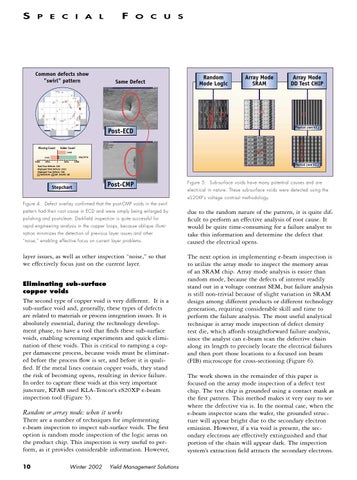
Figure 5. Sub-surface voids have many potential causes and are electrical in nature. These sub-surface voids were detected using the eS20XP’s voltage contrast methodology.
Figure 4. Defect overlay confirmed that the post-CMP voids in the swirl pattern had their root cause in ECD and were simply being enlarged by polishing and post-clean. Darkfield inspection is quite successful for rapid engineering analysis in the copper loops, because oblique illumination minimizes the detection of previous layer issues and other “noise,” enabling effective focus on current layer problems.
layer issues, as well as other inspection “noise,” so that we effectively focus just on the current layer. Eliminating sub-surface copper voids
The second type of copper void is very different. It is a sub-surface void and, generally, these types of defects are related to materials or process integration issues. It is absolutely essential, during the technology development phase, to have a tool that finds these sub-surface voids, enabling screening experiments and quick elimination of these voids. This is critical to ramping a copper damascene process, because voids must be eliminated before the process flow is set, and before it is qualified. If the metal lines contain copper voids, they stand the risk of becoming opens, resulting in device failure. In order to capture these voids at this very important juncture, KFAB used KLA-Tencor’s eS20XP e-beam inspection tool (Figure 5).
Random or array mode: when it works There are a number of techniques for implementing e-beam inspection to inspect sub-surface voids. The first option is random mode inspection of the logic areas on the product chip. This inspection is very useful to perform, as it provides considerable information. However, 10
Winter 2002
Yield Management Solutions
due to the random nature of the pattern, it is quite difficult to perform an effective analysis of root cause. It would be quite time-consuming for a failure analyst to take this information and determine the defect that caused the electrical opens. The next option in implementing e-beam inspection is to utilize the array mode to inspect the memory areas of an SRAM chip. Array mode analysis is easier than random mode, because the defects of interest readily stand out in a voltage contrast SEM, but failure analysis is still non-trivial because of slight variation in SRAM design among different products or different technology generation, requiring considerable skill and time to perform the failure analysis. The most useful analytical technique is array mode inspection of defect density test die, which affords straightforward failure analysis, since the analyst can e-beam scan the defective chain along its length to precisely locate the electrical failures and then port those locations to a focused ion beam (FIB) microscope for cross-sectioning (Figure 6). The work shown in the remainder of this paper is focused on the array mode inspection of a defect test chip. The test chip is grounded using a contact mask as the first pattern. This method makes it very easy to see where the defective via is. In the normal case, when the e-beam inspector scans the wafer, the grounded structure will appear bright due to the secondary electron emission. However, if a via void is present, the secondary electrons are effectively extinguished and that portion of the chain will appear dark. The inspection system’s extraction field attracts the secondary electrons.