D efect M anagement Cross-Channel Rules-Based Binning
With two darkfield angles of incidence and two independent darkfield collectors, plus the brightfield (DIC) subsystem, the new inspector has a total of five distinct data channels (Figure 5). The dual-scan capability means that multiple-channel data can readily be collected on every wafer. Ratios of defect sizing by various channels can be used as attributes for rules-based binning (RBB), providing new capability to distinguish among defect types. Normal
BF DIC
Narrow
Wide
Oblique
Figure 5: Dual scan capability of the Surfscan SP2XP collects inspection data from all five channels. These data are used as defect attributes for advanced binning, using logical and comparison rule-based algorithms.
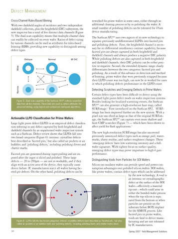
Actionable LLPD Classification for Prime Wafers
Large light point defect (LLPD) is an empirical defect classification referring to any defect captured by both brightfield and darkfield channels by an unpatterned wafer inspection system such as a Surfscan. Defect review shows that LLPDs fall into two broad categories (Figure 6): intrinsic crystalline defects best described as ‘faceted pits,’ but also called air pockets or air bubbles; and ‘polishing defects,’ including polishing divots and chatter marks. Faceted pits are generated during ingot pulling and are exposed after the ingot is sliced and polished. These large defects — 20 to 200µm — are not re-workable, and if they align with an active area of the device, they typically cause device failure. IC manufacturers reject all wafers having faceted-pit defects. On the other hand, polishing defects can be
reworked for prime wafers in some cases, either through an additional cleaning process or by re-polishing the wafer. A small number of polishing defects can be tolerated for 45nm device manufacturing. The Surfscan SP2XP uses two aspects of its new technology to separate previously undifferentiated LLPDs into faceted pits and polishing defects. First, the brightfield channel is necessary for its differential interference contrast capability, because faceted pits are always captured in both brightfield and darkfield channels and always produce a negative DIC polarity. While polishing defects are also captured in both brightfield and darkfield channels, their DIC polarity can be either positive or negative. Second, the extended dynamic range clearly differentiates between the two categories: faceted pits and polishing. As a result of this advance in detection and method of binning, prime wafers that were previously scrapped because their LLPD count was too high, can now be re-worked for cases in which polishing defects predominate in the LLPD count. Detecting Scratches and Emerging Defects in Prime Wafers
Certain defect types have been difficult to detect using the standard light point defect mode on wafer inspection systems. Besides looking for localized scattering events, the Surfscan SP2XP can also generate a high-resolution haze map, called SURFimage.2 First introduced on the Surfscan SP2, SURFimage has been improved further on the new system. With a pixel size one-third as large as that of the original SURFimage, the Surfscan SP2XP can capture even more shallow and faint CMP scratches (Figure 7) — which have been shown to affect yield for flash applications.3 The new high-resolution SURFimage has also uncovered previously unnoticed defect types such as orange peel, watermarks, slurry residue, and surface roughness changes. These ‘emerging defects’ have low scattering intensity and a fullwafer signature. With tighter focus on surface quality, emerging defect types may prove important to high k gate performance. Distinguishing Voids from Particles for SOI Wafers
Silicon-on-insulator wafers can provide speed and power consumption advantages over polished silicon wafers. SOI wafers, like prime wafers, contain defect types which can be addressed by the new technology. A void is an intrinsic or crystallographic defect at the surface of the SOI wafer—effectively a material rip-out—which could arise in either the bonded-wafer process when the top silicon is separated from the bottom or when particles are present on the substrate before BOX implant for the SIMOX process. Like faceted pits in prime wafers, voids are fatal to device manuFigure 6: LLPDs fall into two broad categories: intrinsic crystalline defects best described as ‘faceted pits,’ but also facturing and are not tolerated called air pockets or air bubbles (red); and ‘polishing defects,’ including polishing divots and chatter marks (blue). by IC manufacturers.
30
Spring 2007 Yield Management Solutions