D efect M anagement and the wafer substrate affect the way the defect scatters light, normal and oblique incidence angles, narrow and wide collection channels, and selectable polarizations provide flexibility to capture all defect types. Brightfield Differential Interference Contrast (DIC) Channel
While all Surfscan SPx systems provide darkfield inspection, as described above, the new system incorporates a brightfield channel as well. (Darkfield detection relies on light scattered out of the direct beam, while brightfield detection makes use of the direct beam.) The brightfield channel not only provides another means of detecting challenging defect types, it also includes a DIC capability.1 This technique makes use of the phase of the laser beam to distinguish concave from convex defects. The DIC signal polarity is useful as a descriptor for defect classification.
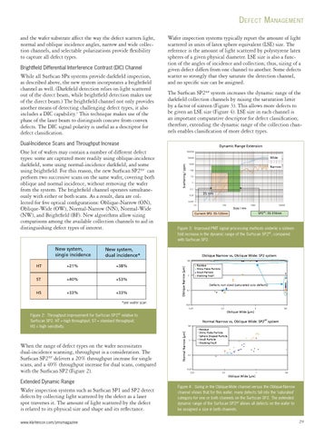
Wafer inspection systems typically report the amount of light scattered in units of latex sphere equivalent (LSE) size. The reference is the amount of light scattered by polystyrene latex spheres of a given physical diameter. LSE size is also a function of the angles of incidence and collection; thus, sizing of a given defect differs from one channel to another. Some defects scatter so strongly that they saturate the detection channel, and no specific size can be assigned. The Surfscan SP2XP system increases the dynamic range of the darkfield collection channels by raising the saturation limit by a factor of sixteen (Figure 3). This allows more defects to be given an LSE size (Figure 4). LSE size in each channel is an important comparative descriptor for defect classification; therefore, extending the dynamic range of the collection channels enables classification of more defect types.
Dual-Incidence Scans and Throughput Increase
One lot of wafers may contain a number of different defect types: some are captured more readily using oblique-incidence darkfield, some using normal-incidence darkfield, and some using brightfield. For this reason, the new Surfscan SP2XP can perform two successive scans on the same wafer, covering both oblique and normal incidence, without removing the wafer from the system. The brightfield channel operates simultaneously with either or both scans. As a result, data are collected for five optical configurations: Oblique-Narrow (ON), Oblique-Wide (OW), Normal-Narrow (NN), Normal-Wide (NW), and Brightfield (BF). New algorithms allow sizing comparisons among the available collection channels to aid in distinguishing defect types of interest.
Figure 3: Improved PMT signal processing methods underlie a sixteenfold increase in the dynamic range of the Surfscan SP2XP, compared with Surfscan SP2.
Figure 2: Throughput improvement for Surfscan SP2XP relative to Surfscan SP2. HT = high throughput; ST = standard throughput; HS = high sensitivity.
When the range of defect types on the wafer necessitates dual-incidence scanning, throughput is a consideration. The Surfscan SP2XP delivers a 20% throughput increase for single scans, and a 40% throughput increase for dual scans, compared with the Surfscan SP2 (Figure 2). Extended Dynamic Range
Wafer inspection systems such as Surfscan SP1 and SP2 detect defects by collecting light scattered by the defect as a laser spot traverses it. The amount of light scattered by the defect is related to its physical size and shape and its reflectance. www.kla-tencor.com/ymsmagazine
Figure 4: Sizing in the Oblique-Wide channel versus the Oblique-Narrow channel shows that for this wafer, many defects fall into the ‘saturated’ category for one or both channels on the Surfscan SP2. The extended dynamic range of the Surfscan SP2XP allows all defects on the wafer to be assigned a size in both channels.
29