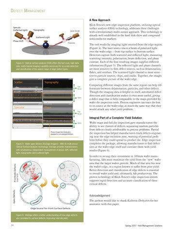
D efect M anagement A New Approach Specula (reflected light)
Topography
Laser Diode
Scattered Light Phase Shift
Polarizer
Figure 4: Optical surface analysis (OSA) offers the fast scan, high data rate, multi-channel imaging capability necessary for accurate detection and classification of the widest range of edge defect types.
Scatter
Topography Top Bevel
Apex
Specular
Phase
KLA-Tencor’s new edge inspection platform, utilizing optical surface analysis (OSA) technology, addresses these challenges with a revolutionary multi-sensor approach. This technology is already well established in the hard disk drive and compound semiconductor markets. The tool works by imaging light emitted from the edge region (Figure 4). The laser source traces a beam of polarized light over the wafer edge – from top surface to bottom surface. Detectors capture both scattered and reflected light, measuring scattering intensity, polarization, beam deflection, and phase contrast. Each of the four resulting images supplies different information (Figure 5). The reflected light and phase channels are most sensitive to film defect sources, such as delamination, flakes, and residues. The scattered light channel is most sensitive to particle sources, chips, and cracks. Together, the images give a complete picture of the wafer edge. Comparing different images from the same region can help differentiate between delamination, particles, and other defects. Though the imaging data is helpful in itself, automated defect detection and classification makes it even more useful, giving a defect map that is fully comparable to the maps provided by wafer die inspection tools. Process engineers can trace die loss to its source at the wafer edge in much the same way that they would attack any other yield problem.
Top Bevel
Integral Part of a Complete Yield Solution Apex
Phase Image best indicates popped vs. un-popped blisters
(darkfield)
In order to recoup their investment in 300mm wafer manufacturing, fabs must maximize the yield from the “new” wafer area that the larger wafers provide. Much of that area lies near the wafer’s edge, in a region known to suffer from poor yield. Better detection and classification of edge defects is essential to overall wafer yield and, ultimately, fab productivity. The proven technology of KLA-Tencor’s edge inspection system supports rapid detection and accurate classification of these critical defects.
Apex Defects
Frontside Defects
Figure 5: Wafer apex blisters (VisEdge images) – With its multi-sensor Optical Surface Analyzer technology, VisEdge provides manufacturers with simultaneous independent measurement of phase shift, reflected light, topographic and scattered light.
Wafer maps and full die inspection gave manufacturers the ability to see clusters of defects, separating random particles from defects clearly attributable to process problems. Partial die inspection has helped manufacturers track defects originating near the edge exclusion zone, warning of potential problems before they could spread to product die. Edge inspection completes the package, allowing manufacturers to find defect sites at the wafer edge itself and correlate them with yield results (Figure 6).
Acknowledgement
The authors would like to thank Katherine Derbyshire for her assistance with this paper. Edge Source for Front Surface Defects Figure 6: VisEdge offers a better understanding of how edge defects are correlated to surface defects, improving total die yield.
20
Spring 2007 Yield Management Solutions