International Research Journal of Engineering and Technology (IRJET) Volume: 06 Issue: 05 | May 2019
www.irjet.net
e-ISSN: 2395-0056 p-ISSN: 2395-0072
2. RESULTS AND DISCUSSION As we know that scaling the MOSFET below sub-20nm node will increase the DIBL value, sub-threshold slope, gate leakage, this is due to decreased gate coupling to the channel. These parameters are important for the performance of a device. Therefore it is necessary to reduce these above mentioned values. In this the doping concentration are varied so that improved performances are obtained. Firstly a device is designed which is explained below In order to design a 10 nm Double gate MOSFET. It is important to make its geometry first in which various regions are well defined like source, drain, gate, body, Oxide. The doping is done in the source, drain and substrate regions. The materials of these regions are given in the table I below .while the Table 2 shows various parameters and there values that we use in this device. Table -1: Regions and materials used in MOSFET Region
Material
Source/drain
Al
Substrate
Silicon
Gate
n-poly Si
Oxide
SiO2
Table -2: Parameters and their values of MOSFET Parameter
Length/T hickness
Mesh conc.
Size/Doping
Gate length
10 nm
Mesh size=.01
Parameter
20nm
Mesh size=.005 1 1015cm-3(acceptor)
Source/drain
5nm
1 1021cm-3(donor)
Oxide(SiO2)
2nm
Mesh size=.01
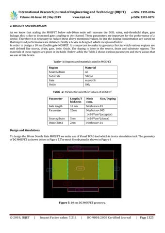
Design and Simulations To design the 10 nm Double Gate MOSFET we make use of Visual TCAD tool which is device simulation tool. The geometry of DG MOSFET is shown below in Figure 5.The mesh file obtained is shown in Figure 6
Figure 5: 10 nm DG MOSFET geometry.
Š 2019, IRJET
|
Impact Factor value: 7.211
|
ISO 9001:2008 Certified Journal
|
Page 1325