METAL POWDERS AND SUSTAINABILITY
WAYLAND ADDITIVE: EVOLVING PBF-EB
AUTOMATING THE AM WORKFLOW


Vol. 10 No. 1 SPRING 2024



in Powder. High performance metal powders. Designed for precision, performance, and innovation.
look.
Unwavering Quality.
Advanced Material Technologies Inc. (Formerly known as Praxair Surface Technologies)
TRUFORM™ metal powders are custom-designed
AM industries and trusted by leading
in aerospace, medical, energy, and industrial markets. With a broad product portfolio that includes custom alloys, we’re always pushing the boundaries of innovation in our R&D additive lab. Making our world more productive TruForm@linde.com | www.linde-amt.com Print the future today.
Precision
New Name. New
Same
Linde
Our
for
OEMs
Discover the Future of Additive Manufacturing with Linde Advanced Material Technologies.
Come visit us in booth #2554 and also attend our technical presentation during the show on: High Strength – High Temperature ODS Materials for AM June 25 - 27, 2024, Los Angeles, CA
Publisher & Editorial Offices
Inovar Communications Ltd
11 Park Plaza
Battlefield Enterprise Park
Shrewsbury SY1 3AF United Kingdom
Tel: +44 (0)1743 469909
www.metal-am.com
Managing Director & Editor
Nick Williams, nick@inovar-communications.com
Group News Editor
Paul Whittaker, paul@inovar-communications.com
Advertising Sales Director
Jon Craxford
Tel: +44 (0)207 1939 749 jon@inovar-communications.com
Assistant News Editor
Charlie Hopson-VandenBos charlie@inovar-communications.com
Editorial Assistant
Amelia Gregory, amelia@inovar-communications.com
Technical Consultant
Dr Martin McMahon
Digital Marketer
Mulltisa Moung, mulltisa@inovar-communications.com
Production Manager
Hugo Ribeiro, hugo@inovar-communications.com
Operations & Partnerships Manager
Merryl Le Roux, merryl@inovar-communications.com
Office & Accounts Manager
Jo Sheffield, jo@inovar-communications.com
Subscriptions
Metal Additive Manufacturing is published on a quarterly basis as either a free digital publication or via a paid print subscription. The annual print subscription charge for four issues is £150.00 including shipping. Rates in € and US$ are available on application.
Accuracy of contents
Whilst every effort has been made to ensure the accuracy of the information in this publication, the publisher accepts no responsibility for errors or omissions or for any consequences arising there from. Inovar Communications Ltd cannot be held responsible for views or claims expressed by contributors or advertisers, which are not necessarily those of the publisher.
Advertisements
Although all advertising material is expected to conform to ethical standards, inclusion in this publication does not constitute a guarantee or endorsement of the quality or value of products or of the claims made by its manufacturer.
Reproduction, storage and usage
Single photocopies of articles may be made for personal use in accordance with national copyright laws. All rights reserved. Except as outlined above, no part of this publication may be reproduced, modified or extracted in any form or by any means without prior permission of the publisher and copyright owner.
Design and production
Inovar Communications Ltd.
ISSN: 2057-3014 ( PRINT )
ISSN: 2055-7183 ( ONLINE )
This magazine is also available for free download from www.metal-am.com
© 2024 Inovar Communications Ltd

Europe’s challenge
At this year’s AM Forum Berlin, AMPOWER’s opening presentation outlined the global business situation for AM machine producers: in short, Asia is seeing strong growth, the US is seeing some growth and European growth has plateaued.
With these statements echoing in the room, the panel discussion that followed was billed as ‘The global battle for 3D printing dominance’ and was even more revealing than the name suggested. The panel consisted of senior figures from Europe and the US, so, in the absence of representation from Asia, there was perhaps a subtle clue as to who this ‘battle’ for dominance might be between.
The discussions that followed were frank and balanced, with participants seeking to pull back from any conflict theme as implied by the panel title, and instead drilling deeper into what is a far more complex a situation for Europe than simply fierce competition from Asia.
What was suggested is that many of the current difficulties faced by Europe’s AM industry have as much to do with internal business and political environments as they do with competition from overseas. Difficulties accessing investment for growth in Europe, it was suggested, is stifling the AM industry and entrepreneurship — this in stark contrast to China and the US, where, despite very different forms of financing, risks are taken.
This is further compounded by a seeming lack of political willingness in Europe to back Additive Manufacturing on a large scale. The obvious point of comparison was with America Makes, which has put a spotlight on this particular sector in the US, and has been backed by a stream of funding for growth. With Europe lacking an equivalent, there is a real risk that it could soon lose its leadership position in an industry it was instrumental in creating.
So, what’s the future for Europe’s Additive Manufacturing industry? Despite the international competition, the power to evolve, at least for now, rests in Europe’s own hands.
Nick Williams Managing Director

Cover image
Inside 6K Additive’s UniMelt® microwave plasma system (Courtesy 6K Additive)

GETPDF 3 METAL ADDITIVE
Metal Additive Manufacturing | Spring 2024
MANUFACTURING
“With our new (WarpSPEE3D) production capabilities, we’ve been able to access multiple multi-million-dollar
And we’ve been able to secure prototyping and production contracts with three Fortune 50 companies. This has been a huge advantage for cash flow over the smaller R&D contracts that we were seeing before.”
Jeremy Schreiber, Co-Founder and CTO/CDO at HAMR Industries LLC.
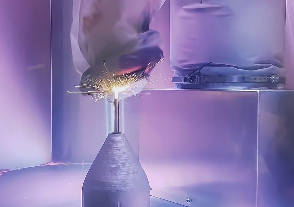

Advance your research with SPEE3D Cold Spray Additive Manufacturing Technology Explore novel alloys, qualified metals, or multi-material blends that haven’t been invented yet—all in record time. Learn more at www.spee3d.com, or find us at RAPID+TCT 2024, Create new research opportunities
with industry partners
workforce grants
Collaborate
Access
contracts.

Contents
127 Metal powders in Additive
Manufacturing: An exploration of sustainable production, usage and recycling
Sustainability has risen to the top of the global manufacturing agenda. Whilst metal AM has long been considered a green technology because of its net-shape capabilities, it is far from being a process absent of environmental impact.
Here, Martin McMahon explores how global efforts are being made to improve this through the use of more sustainable metal powders, combined with a greater focus on powder reuse and recycling. Inextricably linked to this are, of course, economic gains and, in terms of supply chain, national security benefits. >>>
107
143
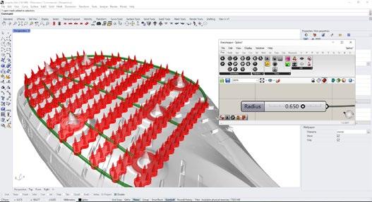
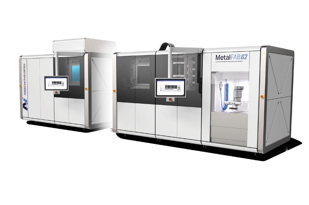
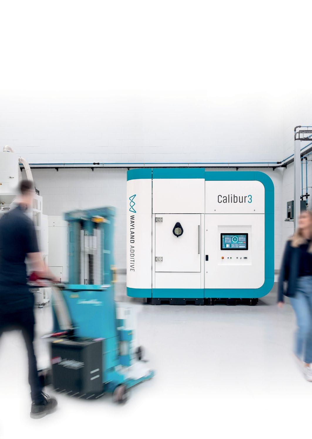
141 Inside Wayland Additive: How innovation in electron beam PBF is opening new markets for AM
UK-based Wayland Additive is convinced that, when it comes to metal Additive Manufacturing, Electron Beam Powder Bed Fusion (PBF-EB) has a bright future ahead. Whilst laser-based PBF is the most widely commercialised AM technology, it has inherent limitations that electron beam-based innovations such as Wayland’s NeuBeam process promise to overcome.
Rachel Park reports on how the technology could open up the AM market by enabling users of the Calibur3 machine to rapidly develop and commercialise a wider range of industrial materials.

GETPDF Metal Additive Manufacturing | Spring 2024 5 Vol. 10 No. 1 © 2024 Inovar Communications Ltd
Vol. 8 No. 3 © 2022 Inovar Communications Ltd
Regular features... 11 Industry news >>> 194 Events guide >>> 197 Advertisers’ index & buyer’s guide >>>
>>>

155 An end-to-end production case study: Leveraging data-driven machine learning and autonomous process control in AM
For Additive Manufacturing to mature as an industrial production process, believe Tommaso Tamarozzi (Oqton) and Juan Carlos Flores (Baker Hughes), it needs to be faster, simpler, and more reliable. This article reports on a step toward this goal through the development of an end-to-end AM workflow for the serial production of a Variable Resistance Trim (VRT) component.
Built on a fully digital framework, it includes simulation, real-time process monitoring, anomaly analysis, and data preparation automation, thus laying the foundation for an AM workflow that delivers consistent quality and the documentation necessary for certification. >>>

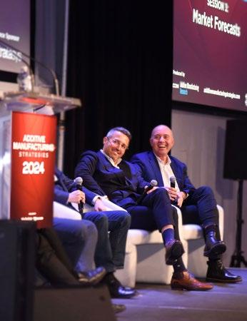
167 Consolidation, competition, and the cost of certification: Insight from New York’s AM Strategies 2024
Additive Manufacturing conferences rarely attract as many industry CEOs as New York’s Additive Manufacturing Strategies event, let alone persuade them to share the stage for panel discussions.
AMS2024 was no exception. On the back of a turbulent financial year for many of the industry’s leading companies, how do those very CEOs see the state of the industry now, and what do they see as the biggest challenges ahead?
Rachael Dalton-Taggart reports for Metal AM magazine. >>>
GETPDF Metal Additive Manufacturing | Spring 2024 7 Vol. 10 No. 1 © 2024 Inovar Communications Ltd
www.metal-am.com/subscribe-to-the-metaladditive-manufacturing-e-newsletter TO OUR NEWSLETTER SUBSCRIBE


Quality, Experience and Customer Relationships
We are driven by these values.


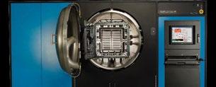
Elnik’s innovations and experiences in all areas of temperature and atmosphere management have led us to become the leaders for the Batch-based Debind and Sinter equipment industry. We have applied these core competencies across a wide variety of industries through our 50 year history and look forward to the emergence of new technologies that will continue to drive demand for new innovative products.
We offer:
First Stage Debind Equipment (Catalytic, Solvent, Water)
Debind & Sinter Furnaces (All Metal or Graphite)
Elnik’s experienced team is driven to be the only partner you need for all your MIM and Metal AM equipment for 2024 and beyond.

12004 Carolina Logistics Drive - Suite A | Pineville, NC 28134 USA | +1 973.239.6066 | elnik.com
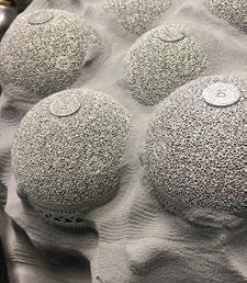
177 Scandium’s impact on the Additive Manufacturing of aluminium alloys
The future of Additive Manufacturing lies in part production at scale. Innovation must, therefore, focus on how to reduce part cost and improve performance. Unlike other manufacturing processes, weight is time in AM – and time is money; raw material costs take a back seat when it comes to overall part cost. Here, Jonathan Meyer (APWORKS) and John Barnes (Metal Powder Works/The Barnes Global Advisors) explore the case for scandium-based aluminium alloys for AM from both technical and economic perspectives. >>>
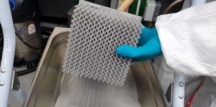
185 AM for medical implants: An analysis of the impact of powder reuse in Powder Bed Fusion
The growing use of titanium Additive Manufacturing for the production of medical implants is a major success story for the industry. With this growth, however, come vast volumes of process data which need to be monitored to ensure compliance with tight regulatory requirements. Here, Peter Lindecke, amsight GmbH, explains how holistic analysis software can be used to monitor the impact of powder reuse strategies in Electron Beam Powder Fusion to ensure the best possible outcomes. >>>
11
194
197
In the digital edition of Metal AM magazine, available at www. metal-am.com, simply click on a company name to view its advert, or on the weblink to go directly to its website. >>>

GETPDF Metal Additive Manufacturing | Spring 2024 9 Vol. 10 No. 1 © 2024 Inovar Communications Ltd Regular features...
Industry news >>>
Events guide >>>
Advertisers’ index & buyer’s guide
advertisers’ index serves as a convenient guide to suppliers of AM machines, materials, part manufacturing services, software and associated production equipment.
Our
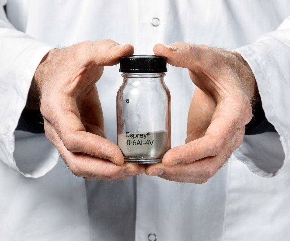
Osprey® online The metal powder webshop
Imagine being able to order Osprey® metal powders at any time, from any device. Imagine hassle-free ordering, fast shipping, and premium quality straight from the source. Osprey® Online is open for business – stocked with powders and expertise! And now we’ve made the check-out process easier, accepting credit card payment for even faster expediting. Browse our online alloy selection optimized for additive manufacturing, including titanium, maraging steel, nickel-based superalloys, and stainless steels. Just add to cart, and we’ll ship within 48 hours!
Shop now metalpowder.sandvik/ospreyonline
Metal Additive Manufacturing | Summer 2021 10 © 2021 Inovar Communications Ltd Vol. 7 No. 2
Industry news
GE Aerospace to invest $161M in US Additive Manufacturing facilities
GE Aerospace has announced plans to invest $650 million in its manufacturing facilities and supply chain in 2024, with the aim of increasing production and improving quality to better support its commercial and defence customers. The plans include some $161 million investment in its Additive Manufacturing facilities located in Alabama and Ohio.
“As GE Aerospace prepares to become a standalone company this spring, we are making significant investments in the future of flight and in the dozens of communities and supplier partners helping us build it,” stated H Lawrence Culp, Jr, chairman and CEO of GE and CEO of GE Aerospace. “These investments are part of the next chapter for GE Aerospace, supporting cutting-edge equipment and safety enhancements that will help us meet our customers’ growing needs.”
GE Aerospace will allocate $54 million to its Auburn, Alabama, site. This will include additional Additive Manufacturing machines and tooling to increase the production of military rotorcraft engine components, along with narrow and widebody commercial aircraft engines.
The company also announced that some $107 million will go to facilities in the greater Cincinnati, Ohio, region. This will see the addition of more Additive Manufacturing machines, new tooling and equipment, and modernisation/upgrades to test cells. This is intended to increase the production capacity of engines in commercial aircraft as well as in US and allied military helicopters and fighter jets.
“This is an investment in the future of manufacturing, ensuring we can continue producing high-quality,
cutting-edge engines and services while meeting customer demand,” said Mike Kauffman, GE Aerospace Supply Chain Vice President.
In total, some $450 million will be put towards new machines, inspection equipment, building upgrades, and new test cells and safety enhancements at twenty-two GE Aerospace facilities across fourteen US states. A further $100 million is allocated to US supplier partners and $100 million at some of its international sites in North America, Europe and India.
In addition to the investments, GE Aerospace announced it is hiring more than 1,000 employees for open external positions at its US factories. www.geaerospace.com
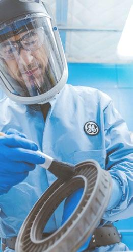
GE Aerospace is investing in its Additive Manufacturing facilities (Courtesy GE Aerospace)
GKN Aerospace’s £50 million boost for its Additive Manufacturing
GKN Aerospace has invested £50 million to expand its Additive Manufacturing capabilities at its site in Trollhättan, Sweden. Set to be operational later in 2024, the new facility is expected to deliver more sustainable aero-engine components by significantly reducing the use of raw materials by up to 80%.
The Swedish Energy Agency’s Industriklivet initiative will fund £12 million of this investment, with the new AM production centre projected to create around 150 new job opportunities for highly skilled operators, technicians, and engineers at the Trollhättan facility.
With research and technology centres in Sweden, the UK and the US, GKN Aerospace has been utilising Additive Manufacturing for almost two decades. The company reports it currently has AM components on seven flying platforms.
“We are committed to driving sustainability in the aviation industry and pioneering improved solutions for our customers,” stated Joakim Andersson, president of GKN Aerospace’s Engines business. “Our development of additive fabrication for large, complex and load-bearing aircraft components is a great example of this and it marks a significant breakthrough for the industry. The benefits we see from this technology are truly game-changing. Government support has been pivotal in enabling us to push our capabilities forward and I am delighted to establish this unique technology in our world-leading facility in Trollhättan, Sweden.”
www.gknaerospace.com
| contents | news | events | advertisers | website | newsletter | GETPDF Metal Additive Manufacturing | Spring 2024 11 Vol. 10 No. 1 © 2024 Inovar Communications Ltd
Fluent Metal launches with $5.5M funding for its liquid metal Additive Manufacturing technology
Fluent Metal, based in Cambridge, Massachusetts, USA, has announced it is developing production-grade liquid metal printing technology for the Additive Manufacturing of functional, sustainable, and economical metal parts. The company recently launched out of stealth, with an additional $3.2 million in venture capital funding, led by E15 with participation from Pillar VC and industry angels, bringing the total funding to $5.5 million.
“Drop-on-demand technology is an elegant approach to create complex metal components,” stated Peter Schmitt, CEO. “Whether it’s prototype iterations of an idea or production runs of a single part, Fluent Metal will provide customers with great operational and material flexibility. This freedom will unlock new creativity and problem-solving abilities across industries.”
The single-step Fluent Metal process uses an inkjet-like
Desktop Metal announces $50M savings plan and 20% workforce reduction
Desktop Metal, Inc., headquartered in Burlington, Massachusetts, USA, has announced a cost-saving plan of $50 million that includes a 20% reduction in its workforce. The move is said to be part of a broader strategic business review aimed at improving its profitability. Other actions include continued consolidation of facilities and product rationalisation.
“The cost-reduction plans announced today, in addition to the $100 million in cost reductions realised in 2023, will help us generate positive cash flow in light of a softer demand environment,” stated Ric Fulop, founder and CEO of
Desktop Metal. “We are committed to getting profitable during this challenging period. The vast majority of the cuts will be completed this quarter, resulting in sequential cost reductions across the first half of 2024.”
“While our industry is working through a challenging period, Desktop Metal’s commitment to its Additive Manufacturing 2.0 vision has not changed. We continue to have a positive long-term outlook for this industry as it transitions to mass production,” Fulop continued.
Desktop Metal has notified US-based employees impacted by the
printhead with wire as the starting material. There is no waste and multi-metal Additive Manufacturing is possible. It is also possible for high-value metals to be intricately combined and complex shapes, such as fully-enclosed voids and internal channels, to be produced.
Fluent Metal’s approach is designed to operate safely on a typical manufacturing floor or even in a prototyping shop, without the need for clean rooms or expensive safety measures. Additionally, material changeover is designed to be easy with a plug-and-play system, reducing setup efforts and allowing for higher machine uptimes.
“As the manufacturing industry evolves in response to the changing needs of global supply chains and sustainability demands, we need novel approaches to drive creativity and expand our collective conception about what’s possible,” shared Philip Liang, Managing Partner, E15. “In the near-term, Fluent Metal will spark the imagination of designers, engineers, and technologists to consider how rapid, on-demand production of custom metal parts could transform their capabilities. At scale, this approach will revolutionise the entire footprint and direction of industrial manufacturing.”
www.fluentmetal.com
cuts. The company is continuing to review modifications to its international workforce, the timing of which will be subject to local regulatory requirements.
This recent action is anticipated to lead to pre-tax restructuring charges of $24.3 million to $31.5 million. The majority of these expected charges are non-cash, with around $5.3 million to $7.5 million of the restructuring charges coming from cash reserves.
Desktop Metal said it is continuing to invest in products and operations in line with near-term revenue generation, positioning the company to achieve its longterm financial goal of sustainable profitability.
www.desktopmetal.com
Metal Additive Manufacturing | Spring 2024 12 © 2024 Inovar Communications Ltd Vol. 10 No. 1 | contents | news | events | advertisers | website | newsletter | Industry News
The Fluent Metal process uses an inkjet-like printhead and wire as the starting material (Courtesy Fluent Metal)

AM METAL POWDER MANUFACTURER Ti64 CHARACTERISTICS Plasma Quality Powder High Sphericity High Purity Traceability Tekna.com W Ta Al ALLOYS Ni ALLOYS
Swiss Steel Group offers range of metal powders for Additive Manufacturing
Swiss Steel Group, headquartered in Lucerne, Switzerland, has announced a range of gas-atomised metal powders developed for the Additive Manufacturing industry. The company is offering powders based on iron, nickel and cobalt as part of its Printdur brand, as well as low- and medium-alloy steels under its Bainidur AM line. A range of nickelfree powders suited to use in medical applications are available under its Medidur AM range.
Iron-based metal powder
The company’s iron-based powders for Additive Manufacturing are divided into austenitic, agehardenable and martensitic grades. The austenitic grade Printdur 4404 is reported to provide high corrosion resistance and good oxidation resistance. Printdur 4545 and Printdur 4548 are focused on the combination of wear, corrosion and oxidation properties. Printdur Powderfort, Printdur 2343 and Printdur 2344 are suitable choices for increased wear resistance.
Nickel-based metal powder
Nickel-based metal powders, suited for applications that require high corrosion resistance, include Printdur Ni625. This alloy is said to offer good resistance to mineral acids, such as nitric, phosphoric, sulphuric or hydrochloric acid, and is also corrosion-resistant to alkalis and organic acids. Furthermore, in the solutionannealed condition, the material has good resistance to hot gas corrosion and high creep rupture strength above 600°C.
Cobalt-based metal powder
Printdur CoCrF7 is a cobaltbased metal powder that can be used in both high-temperature applications and medical technology. Printdur CoCrF75 reports excellent resistance to thermal shock and is resistant to oxidising and reducing atmospheres up to approximately 1,150°C. Its properties also include very good biocompatibility and corrosion resistance.
Kennametal joins ModuleWorks partner programme for intelligent manufacturing
Kennametal Inc, based in Pittsburgh, Pennsylvania, USA, has joined ModuleWorks’ Strategic Partner Program. The network is focused on driving intelligent and integrated digital manufacturing solutions and Kennametal accompanies a range of industry leaders, such as Mitsubishi Electric, AutoDesk, PTC and DMG Mori.
“This partnership combines our robust application knowledge and materials science expertise with ModuleWorks’ industry-leading software to deliver solutions that are technologically advanced and user-friendly, further supporting the evolving needs of our customers,”
stated Sanjay Chowbey, president of Metal Cutting division.
Kennametal’s focus on the computer-aided manufacturing (CAM) market also addresses customer challenges, including the evolving workforce, creating a greater need for technical support helping customers machine with greater precision and efficiency while effectively reducing costs.
Dr Yavuz Murtezaoglu, founder and Managing Director of ModuleWorks added, “We are excited to welcome Kennametal to the Strategic Partner Program. The programme gives solution providers the software development resources they need to
Bainidur AM
The Bainidur AM line expands Swiss Steel Group’s portfolio of metal powders with low- and medium-alloy steels. These are intended to enable fast and efficient Additive Manufacturing of initial samples that also exhibit the subsequent component properties. Heat treatment and thermochemical surface treatments can be tested and optimised with the same material as in series production.
This line also supports the production of spare parts for which the original forging die is no longer available, due, in part, to the good conversion behaviour in the bainite structure.
Medidur AM
The newly-developed material, Medidur, is an austenitic, patent-pending steel powder for Additive Manufacturing. The use of manganese is said to eliminate the need for nickel. The material is non-magnetic, corrosion-resistant and offers high strength, said to make it advantageous for a range of medical applications.
www.swisssteel-group.com
Kennametal offers a range of metal Additive Manufacturing services (Courtesy Kennametal)
empower their digitalisation strategies and collectively advance automation in the manufacturing industry. As a cutting tool manufacturer, Kennametal extends the variety of partners in the programme, thereby further driving the digitalisation initiative in the industry.”
www.kennametal.com
www.moduleworks.com
Metal Additive Manufacturing | Spring 2024 14 © 2024 Inovar Communications Ltd Vol. 10 No. 1 | contents | news | events | advertisers | website | newsletter | Industry News
BUILD PARTS BIGGER,
Maximize
ARCEMY® delivers:
• Superior-quality metal parts that meet rigorous industry standards.
• Unmatched design freedom for fabricating complex, mission-critical parts.
• Reduced lead times and production costs compared to traditional methods.
• Minimized waste through efficient material utilization. Contact us today to discuss how ARCEMY® can transform your mission-critical

Increase manufacturing productivity with ARCEMY® .
efficiency
3D
and performance in your Aerospace, Defense, Maritime, and Oil & Gas operations with ARCEMY® , a revolutionary metal
printing solution powered by proprietary software and our patented Wire-arc Additive Manufacturing (WAM®) process.
manufacturing, delivering unprecedented efficiency and performance.
2024-03-13 MAM FPAutumun CERTIFIED ADDITIVE MANUFACTURING FACILITY QUALIFICATION A P PROVEDMARITIME MANUFACTUR E R DNV.COM/AF Quality Certified ISO 9001:2015 AU1769B-QC Aus. Pat. 2019251514. JP 7225501. EP 3781344. WAM ®: Wire Additive Manufacturing. AML3D ®, WAM ®, WAMSoft ®, ARCEMY® are all registered trademarks of AML3D Limited. www.aml3d.com Australia | United States of America info@aml3d.com | +61 8 8258 2658
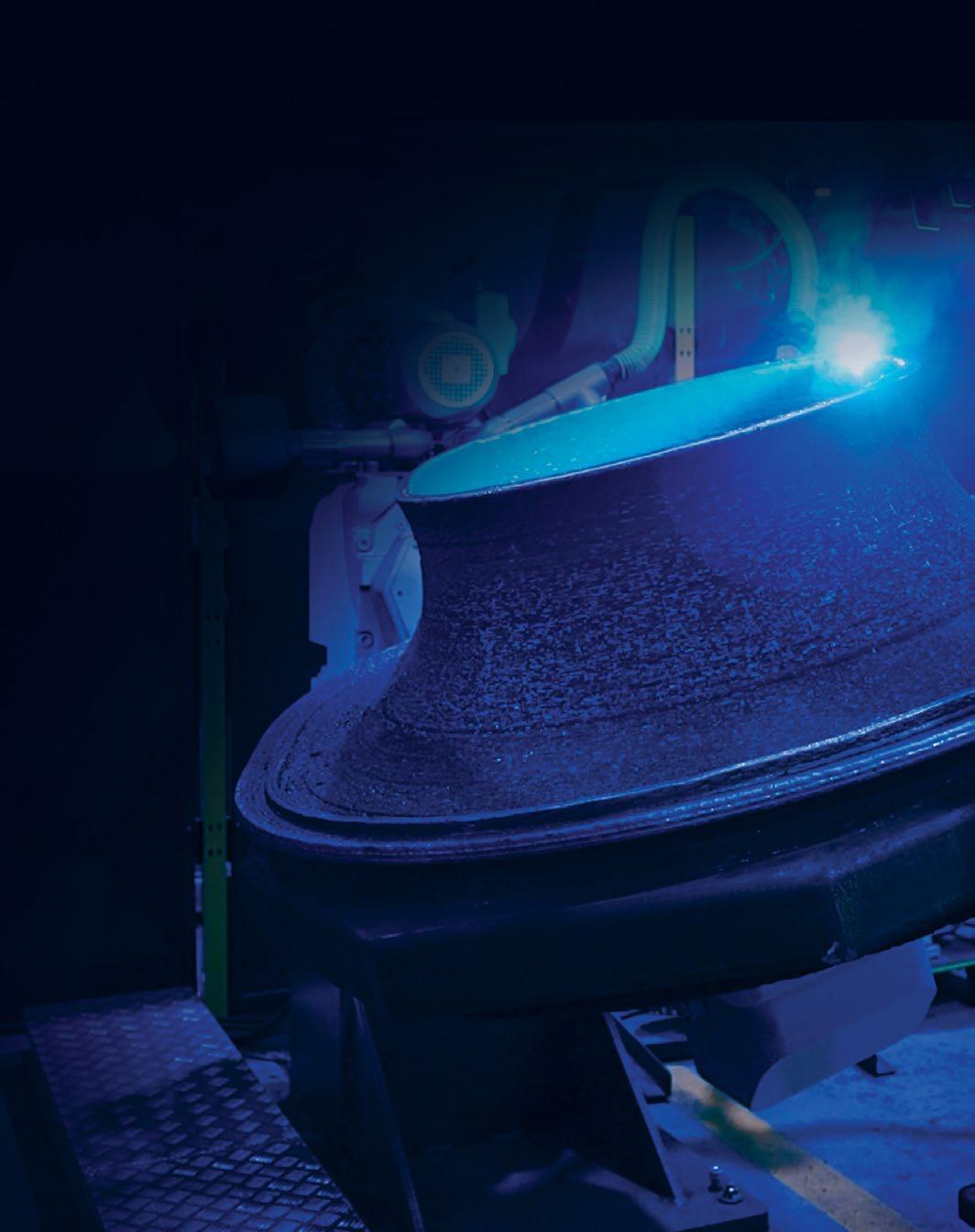
Shown: Panama Chock, ship board fitting. Manufactured with ER70S-6, deposited mass 1.25 tonne, size 1,500 x 1,290 x 540 mm, total print time 188 hrs.
STRONGER, FASTER & GREENER with

Plastometrex and Renishaw aim to increase analysis and part confidence in Additive Manufacturing testing
Plastometrex, a developer of mechanical testing solutions based in Cambridge, UK, reports it has supplied Additive Manufacturing machine maker Renishaw with its proprietary Profilometry-based Indentation Plastometry (PIP) technology. The collaboration focuses on incorporating the enhanced capabilities of PIP into Renishaw’s testing processes, in an effort to increase the precision and efficiency of mechanical property analysis and part confidence in Additive Manufacturing.
Tensile testing in the AM sector presents several challenges: First, the time and material required to produce tensile coupons take up significant chunks of project timelines and budgets, while the use of separately additively manufactured tensile coupons may fail to fully represent the mechanical properties of complex additively manufactured parts, potentially affecting the reliability of data.
Renishaw’s adoption of Plastometrex’s PIP testing is intended to tackle these challenges. The PLX-Benchtop facilitates rapid, direct testing on different sections of AM parts, delivering comprehensive stressstrain curves in minutes. This method provides a more precise evaluation of a part’s mechanical properties and complements Renishaw’s existing testing procedures.
Benjamin Haigh, Materials Scientist at Renishaw, commented, “We can now use cubes built for product development for additional testing, saving us time and money. Additionally, the PLX-Benchtop can generate mechanical data for a wider range of parameters.”
By enabling users to directly test an additively manufactured part (and in several different locations), the PLX-Benchtop equips Renishaw with a more detailed understanding of the mechanical properties of a part while streamlining the testing process.
The test itself is largely automated, taking under five minutes and requiring minimal sample prep. Furthermore, by bypassing the need for coupons and associated material and machining, Renishaw hopes to benefit from mechanical testing cost and time savings.
Jed Robinson-Wall, Materials Science graduate, added, “PIP tech -

nology is a fantastic complement to our existing mechanical testing regime. It gives us even greater insight into the quality of parts produced on our RenAM 500 series of metal Additive Manufacturing systems.”
This collaboration not only surmounts the traditional limitations of tensile testing but also sets a new standard for accuracy and efficiency in mechanical property analysis for Additive Manufacturing.
www.plastometrex.com
www.renishaw.com


Metal Additive Manufacturing | Spring 2024 17 Vol. 10 No. 1 © 2024 Inovar Communications Ltd | contents | news | events | advertisers | website | newsletter | GETPDF Industry News
3DEO secures investment from Seiko Epson and Development Bank of Japan
3DEO, headquartered in Los Angeles, California, USA, has announced a significant investment from the Development Bank of Japan Inc. (DBJ) and Seiko Epson Corporation (Epson), reported to total around one billion yen ($6.8 million).
According to Nikkei Asia, Epson and DBJ participated in a funding round that involved existing investors and, while the full details have not been disclosed, the investment made by the two Japanese companies was believed to account for a roughly 5% stake.
“The collaboration with DBJ and Epson is a powerful endorsement of our mission to empower product and engineering teams across the globe,” stated Matthew Petros, CEO and co-founder of 3DEO. “This investment is not just capital; it’s a commitment to a shared vision of challenging what’s possible through the combination of additive design principles and differentiated capabilities.”
In Japan, there is a strong belief in conventional metalworking based on precision casting, which has supported the growth of the machining and assembly industry, as well as the optimisation of the supply chain in terms of quality and cost. However, while there is a movement toward research and development of AM technologies and DfAM, the adoption rate at production sites faces significant barriers. This collaboration is poised to address these challenges, contributing to

the advancement of AM technologies within Japan’s established manufacturing landscape.
DBJ and Epson’s investment, secured after careful review by the Committee on Foreign Investment in the United States (CFIUS), will enable 3DEO to leverage the Japanese manufacturing industry’s strengths while fostering technological advancements in both regions.
“By integrating 3DEO’s AM capabilities with the meticulous engineering tradition of Japan, we aim to unlock new levels of productivity and expand the manufacturing possibilities in one of the world’s leading economies,” added Payman Torabi, CTO and
co-founder of 3DEO. “This investment is a testament to the trust and potential seen in 3DEO’s innovative approach. We are excited to collaborate with DBJ and Epson, leveraging their expertise and market reach to enhance and refine the landscape of Additive Manufacturing.”
Founded in 2016, 3DEO is an AM service bureau using its in-house patented process it calls Intelligent Layering. The technology is a fusion of Binder Jetting (BJT) and CNC machining that 3DEO claims is faster, cheaper and capable of higher resolution than BJT alone. 3DEO’s unique AM process, and its advanced Design for Additive Manufacturing, is underpinned by a differentiated portfolio of eighteen patents.
www.corporate.epson
www.dbj.jp/en
www.3DEO.co

Metal Additive Manufacturing | Spring 2024 18 © 2024 Inovar Communications Ltd Vol. 10 No. 1 | contents | news | events | advertisers | website | newsletter | Industry News
For Binder Jetting and other sinter-based AM... Read PIM International, our sister publication, for deep dive articles and news covering sinter-based AM technologies. www.pim-international.com
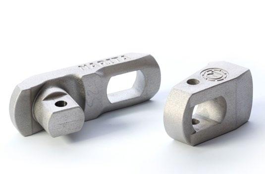
3DEO received a 2023 MPIF Award of Distinction for this fastener assembly used to attach the inter-car baffles to retaining frames on bullet trains (Courtesy MPIF)
CoCr-Alloys Performance in Laser Powder Bed Fusion





1000 Kelvin’s AMAIZE now available as part of Autodesk Fusion 360
1000 Kelvin, headquartered in Berlin, Germany, has announced the availability of its recently launched AMAIZE software as a plug-in for Autodesk’s Fusion integrated CAD/CAM software platform Autodesk Fusion 360.




AMAIZE uses machine learning models informed by physics and manufacturing data to predict design and build issues and then output optimal build files that result in successful builds. As a result, engineers using Additive Manufacturing can eliminate physical trial and error cycles, and handle more complex parts which would otherwise require extensive and time-consuming design iterations.






medical industrial dental

“Availability of AMAIZE on the Autodesk App Store is set to transform manufacturing operations,” said Katharina Eissing, CTO and co-founder of 1000 Kelvin. “This integration will improve manufacturing productivity by increasing uptime, significantly reducing lead times, bolstering process stability, and expediting the training process for staff to gain expertise in 3D printing. I am very excited to partner with Autodesk to democratise Additive Manufacturing.”
These improvements are said to be particularly beneficial for precision Additive Manufacturing companies that are currently facing challenges due to escalating costs and an ageing workforce.
“One of AI’s greatest benefits is its ability to simplify complex processes, expanding access to powerful technology beyond a small circle of domain experts,” stated Stephen Hooper, Autodesk Vice President, Design & Manufacturing Product Development. “By automating the setup and programming of industrial-grade print processes, 1000 Kelvin’s AI, integrated with Autodesk Fusion in the cloud, unlocks the opportunity for a much broader pool of professionals to be successful with Additive Manufacturing. I’m very excited to be offering AMAIZE to Fusion users.”
“One of the main challenges in the manufacturing industry, and especially the US today, is the talent shortage, which is holding companies back from scaling to fulfil fast-growing demand in the market,” shared Omar Fergani, CEO and co-founder of 1000 Kelvin. “Our AI co-pilot AMAIZE is an enabler to overcoming this hurdle, helping companies secure their know-how.”
AMAIZE is now publicly available from the Autodesk App Store.
www.1000kelvin.com
www.autodesk.com
Metal Additive Manufacturing | Spring 2024 20 © 2024 Inovar Communications Ltd Vol. 10 No. 1 | contents | news | events | advertisers | website | newsletter | Industry News
Convince yourself! S&S Scheftner GmbH Dekan-Laist-Straße 52 D-55129 Mainz +49 (0) 61 31-94 71 40 sales@scheftner.dental www.scheftner.dental
Boost print speeds and cut part costs in half.
Unlock greater speed, efficiency, and profitability with high-performance Aluminum powderssame printers, faster production, no compromises.
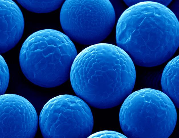
If you want to be a high-performance manufacturer you need to leverage the power, quality, and control of high-performance print materials. Equispheres powders are purpose-built for additive manufacturing. Our unique technology allows us to refine the characteristics of each powder line - optimizing performance for AM production applications.
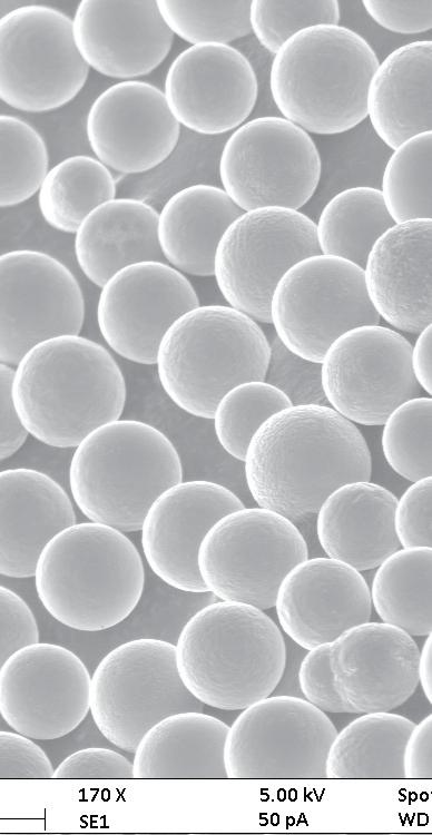
Get in touch to learn about how our high-performance Aluminum powders can improve your printer’s performance, speed up production, and save money on every print.
the future is made of.
equispheres.com | Suite 4100, 500 Palladium Dr. Ottawa, Canada | 1.613.903.5855 | info@equispheres.com
What
EOS, Phillips Federal and Austal USA develop new copper-nickel CuNi30 alloy for Additive Manufacturing
EOS GmbH, located in Krailling, Germany, has announced the development and commercial availability of its new EOS CopperAlloy CuNi30 powder, a copper-nickel alloy engineered specifically for Laser Beam Powder Bed Fusion (PBF-LB) Additive Manufacturing. The copper-nickel alloy was created in partnership with Phillips Federal and Austal USA.
EOS CopperAlloy CuNi30 is said to deliver excellent performance and material properties with a
combination of high strength and ductility, around 510 MPa UTS and more than 20% elongation. The material achieves high corrosion resistance in salt water and sustained performance in low temperatures. With these mechanical properties, EOS claims to have met UNS C96400 specifications as mentioned in ASTM B369-09 for mechanical performance.
Alongside Phillips Federal and Austal USA for the submarine industrial base (SIB), EOS CopperAlloy CuNi30 was developed and tested to alleviate the supply pressure of traditional castings and meet the goal of ‘2+1 Columbia and Virginia Class submarine platforms’ for the US Navy. Phillips Federal has noted that the material’s performance, combined with the competitive cost-per-part (CPP), has created a strong business case for production implementation.
“EOS was provided with a strategic objective to deliver a CuNi30 product to the US Navy submarine industrial base to mitigate casting delays; a material holding unique to the naval construction industry and not widely available for AM technology use. We acted with priority to support the submarine programme schedule,
Oerlikon announces consolidation and relocation of its Additive Manufacturing business to US
Oerlikon, headquartered in Pfäffikon, Switzerland, has announced that it plans to strategically realign its Additive Manufacturing business and consolidate its AM production in the US. The move, whilst acknowledging the US region as the largest growth market for AM technology, is also said to be in response to the adverse market conditions for AM in Germany that Oerlikon states limits growth opportunities.
Focusing AM production in Huntersville, North Carolina, will bring the business closer to the US growth sectors, such as semiconductor, and also enable the business to benefit from the more conducive US framework conditions and higher market acceptance for disruptive technologies. In the future, European and other international customers are planned to be served from the US.
and we are pleased to share our successful product release within a few months of the project start. It is a privilege to contribute to projects of such strategic importance to our national interests,” shared Ankit Saharan, senior manager of metals technology at EOS.
The manufacturing of CuNi alloy components has traditionally involved casting, which can be expensive due to testing and quality requirements. Through the use of Additive Manufacturing and EOS CopperAlloy CuNi30, users can now meet these requirements while also benefitting from the design and production advantages inherent with the AM process.
“We are grateful for the response from EOS and the Additive Minds team to develop EOS CopperAlloy CuNi30 so quickly. This alloy is critical in many marine applications and will be important in our efforts to support the US Navy Center of Excellence,” stated John Harrison, Senior Vice President of Global Additive at Phillips Federal.
EOS CopperAlloy CuNI30 is now commercially available for the midframe EOS M 290 and the large-frame EOS M 400. These will be followed by the four laser EOS M 400-4 later in 2024.
www.usa.austal.com
www.phillipsfederal.com
www.eos.info
In close coordination with existing customers, the company said that its current production at Barleben and Shanghai is planned to be relocated in 2024. The research and development site in Garching, Germany, will focus on developing new advanced materials, surface coating technologies and digitalisation.
Additive Manufacturing is a business of Oerlikon’s Surface Solutions division. The business was founded as a start-up to develop and produce novel 3D applications for sectors such as aerospace and semiconductor, added Oerlikon.
www.oerlikon.com
Metal Additive Manufacturing | Spring 2024 22 © 2024 Inovar Communications Ltd Vol. 10 No. 1 | contents | news | events | advertisers | website | newsletter | Industry News
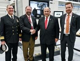
From left: Admiral Scott Pappano; Alan Phillips, president of Phillips Corporation; Carlos Del Toro, Sr., Secretary of the Navy; John Harrison, Sr. Vice President Global Additive at Phillips Federal (Courtesy Phillips Corporation)

Kymera International acquires copper-based powder producer Royal
Metal Powders
Kymera International, a speciality materials company headquartered in Raleigh, North Carolina, USA, has acquired Royal Metal Powders Inc., a manufacturer of water and air-atomised copper-based powders located in Maryville, Tennessee.
Under the continued leadership of Mike Lutheran, president of Royal Metal Powders, Kymera will continue operations at Royal’s facility until all production can be moved to Kymera’s manufacturing sites in North Carolina, Pennsylvania and Germany. It was added that Lutheran will be joining Kymera as Senior Vice President.
“The copper powder markets have encountered headwinds over the past few years, but we remain committed to ensuring Kymera and Royal’s customers receive timely and high-quality supply of these critical materials for decades to come,” stated Barton White, CEO of Kymera. “As demonstrated by our recent $20 million expansion of our North Carolina facility, Kymera is positioned to provide uninterrupted, long-term supply for the entire market.”
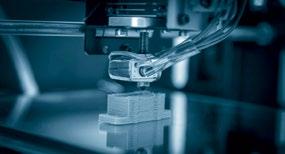


Royal Metal Powders will continue at its Maryville facility until production can be moved to Kymera’s existing facilities (Courtesy Kymera International)
Royal Metal Powders offers a wide variety of powders, including copper, brass, premix and pre-alloyed bronze powders, nickel/silver, tin powder, electrolytic copper powders, lead powders, and phos copper powders.
Adam Shebitz, Partner at Palladium Equity Partners, the parent company of Kymera International, added, “We are pleased that Kymera continues to demonstrate its unwavering commitment towards the copper powder market. Following the recent expansion undertaken at Kymera’s RTP facility, the acquisition of Royal’s assets reinforces Kymera’s position as a well-capitalised and high growth supplier of niche specialty materials.”
www.kymerainternational.com
www.royalmetalpowders.com
Thomas Weissgärber elected co-chair of the European Powder Metallurgy Institute
The European Powder Metallurgy Institutes (EPMI), a Sectoral Group of the European Powder Metallurgy Association (EPMA), has announced Prof Dr-Ing Thomas Weissgärber as co-chair of the EPMI Working Group alongside Adj Prof Dr Dr habil Susanne Norgren. Weissgärber takes over from Prof Elena Gordo following the end of her four-year term in the position.
The EPMI is an association of twenty major European PM research centres. Under the umbrella of the EPMA, the experts support and promote cooperation between industry & research and advocate relevant policies on education and research topics in the field of PM.
Thomas Weissgärber is Director of Fraunhofer IFAM Dresden and has held a professorship in Powder Metallurgy at Technische Universität Dresden since April 2022. He has published over 200 articles and had involvement in over eighteen patent applications. In 2018, he won the Skaupy Prize and, in 2022, the EPMA Fellowship Award.
www.epma.com
Metal Additive Manufacturing | Spring 2024 24 © 2024 Inovar Communications Ltd Vol. 10 No. 1 | contents | news | events | advertisers | website | newsletter | Industry News
Contact Us DIGITISE YOUR AM POWDER MANAGEMENT & WORKFLOWS ALL IN ONE PLACE www.amtrace.com (44) 7802257840 info@amtrace.com Digitally Trace All Metal Powders from virgin through recycling or recovering to build parts and ultimate disposal Ask about our 30 Day Free Trial Available until 30th June 2024

MIM & AM
METAL POWDERS
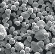
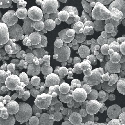
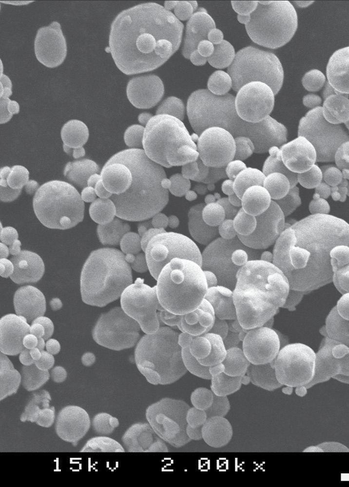
Buy direct from a US producer of fine spherical powders with over 30 years of experience. Ultra Fine uses unique, inert gas atomizing technology to produce spherical metal powders that work in your MIM or metal AM application on a small or large production scale.
Our team has the experience to make your powders, as we have been working with customers to produce standard and custom fine powders for unique applications since 1990! With partner Novamet, Ultra Fine’s high quality powders can be further enhanced through coating or other postatomization treatments. Providing Quality Metal Powders Since 1976

ISO9001:2015CERTIFIED
Toshiba Drive, Suite E Lebanon,
1420
TN 37087 USA www.novametcorp.com
ISO9001:2015CERTIFIED www.ultrafinepowder.com 500 Park East Drive | Woonsocket, RI 02895 USA AS9100:2016 CERTIFIED
Sandvik adds Osprey C18150 CuCrZr for high-temperature applications
Sweden’s Sandvik AB has launched Osprey C18150, a copper-based metal powder tailored for applications which require increased mechanical strength at high temperatures, whilst maintaining high electrical and thermal conductivity. These attributes are said to make the powder suitable for electrical, electronic and thermal transfer components in a variety of industries such as aerospace and automotive.
Osprey C18150 (CuCrZr) is a copper-based alloy that contains
small amounts of chromium and zirconium to balance copper’s high conductivity and heat dissipation capabilities. Thanks to the precipitation of Cr- and Zr-rich particles upon ageing, this balance persists even at elevated temperatures. It can withstand service temperatures up to 500°C.
The alloy has been developed as fine powder for Metal Injection Moulding (MIM) and Binder Jetting (BJT) using Osprey High Yield Technology, but also as a coarser

ADDiTEC and MECHA partner to boost advanced metal manufacturing
ADDiTEC, headquartered in Palm City, Florida, USA, has announced a strategic partnership with MECHA, Inc., Raleigh, North Carolina, which aims to leverage ADDiTEC’s metal Additive Manufacturing technologies with MECHA’s high-volume precision machining and finishing services.
The partnership looks to provide customers with diverse, costeffective end-to-end solutions from technological integration to post-sales support. With MECHA focused on rapid prototyping and ADDiTEC focused on minimised time to market, the companies believe that its partnership will be well-suited to industries such as aerospace, automotive, biotechnology and medical.
“As we join forces with MECHA Inc, we are not just forming a
partnership; we are crafting a synergy of innovation and precision in advanced metal manufacturing,” stated Brian Matthews, founder & CEO of ADDiTEC. “This collaboration allows us to combine ADDiTEC’s groundbreaking technologies with MECHA’s exceptional machining and metal services, promising unparalleled solutions for our clients. Together, we are shaping the future of metal manufacturing with a shared commitment to quality, efficiency, and cutting-edge excellence.”
The partnership is also intended to facilitate collaborative research and development initiatives in an effort to enable the companies to enhance product design and performance. Their joint efforts
powder for Laser Beam Powder Bed Fusion (PBF-LB) and Directed Energy Deposition (DED).
“Our metal powder portfolio continues to grow, and we are very excited about our latest addition, Osprey C18150,” stated Dr Eleonora Bettini, Customer Application Specialist for metal powder at Sandvik. “With our wide range of Osprey C18150 powders, with customised properties and particle size distributions, manufacturers from a variety of industries can enjoy the many benefits that this material has to offer.”
Osprey C18150 is manufactured by inert gas atomisation, producing a powder with a spherical morphology which provides good flow characteristics and high packing density. The powder has been tested and qualified with several customers in different industries and for different applications.
Available via the Osprey Online webshop in Europe and through KBM
Advanced Materials in the US, Osprey C18150 is also available in other fractions and for other manufacturing technologies from Sandvik.
www.metalpowder.sandvik
aim to push the boundaries of what is achievable in advanced metal manufacturing, bringing cuttingedge solutions to clients.
Bobby Boyd, founder and president of Mecha, Inc., added, “At MECHA, we continually push the limits of CNC machining, so we are extremely excited to take things to the next level through our partnership with ADDiTEC, a leader in advanced metal manufacturing. This strategic alignment will allow our respective customers to innovate in ways that were previously inconceivable, while experiencing an unmatched level of service and support for their cutting-edge designs. Metal manufacturing is going to evolve rapidly in the near future because of ADDiTEC’s technology, and we are glad to play a role in that evolution.”
www.additec3d.com
www.mechainc.com
Metal Additive Manufacturing | Spring 2024 26 © 2024 Inovar Communications Ltd Vol. 10 No. 1 | contents | news | events | advertisers | website | newsletter | Industry News
Sandvik’s Osprey C18150 (CuCrZr) powder is available for Additive Manufacturing and Metal Injection Moulding (Courtesy Sandvik)




































































Our ambition: To become net zero by 2037
In the world of metal powders, Höganäs is always at the forefront of innovation.
From more sustainable production processes to new and patented powder compositions, we are dedicated to offering you optimal solutions while reducing environmental impact. With our range of powders designed for additive manufacturing, we can offer powders designed for any application. Combining optimal powder performance with improved sustainability is a priority for Höganäs, as we are on a journey to becoming the world’s first sustainable metal powder producer.
In addition to our material innovations, we have also committed to Science Based Targets and are founding members of the Additive Manufacturing Green Trade Association, demonstrating our ongoing commitment to leading sustainable transformation in our industry.
Scan the QR code to read our 2022 sustainability report
www.hoganas.com
3374HOG
Fastech joins Meltio’s manufacturing partner network in the USA
Meltio, Linares, Spain, has announced that Fastech Inc, Danville, Virginia, USA, has joined its US manufacturing partner network. Fastech is an additive and subtractive manufacturing services company that applies Wire Arc Additive Manufacturing (WAAM), CNC, and reverse engineering techniques to provide an end-to-end manufacturing solution to a variety of industries.
“We at Fastech are excited to start this great partnership with Meltio to continue our growth trajectory,” stated Alan Pearce, CEO of Fastech. “This partnership will enhance our capabilities to provide an ‘End-to-End’ solution for our customers. The Meltio Engine Robot Integration will allow us to print metals in an environment using a six-axis robotic system. This grants us to manufacture very large titanium components, as well as other reactive alloys within this homogeneous environment, assuring the utmost level of quality every day.”
“The ability to undertake a build volume for components up to 6 ft cubed [.17 m 3], using wire and laser can be beneficial in manufacturing thin, more detailed features seamlessly whilst maintaining excellent mechanical properties,” he continued. “Furthermore, our post-processing five-axis machining services, full component 3D dimensional inspection, as well as offering nondestructive and destructive inspection of test specimens, closes the gap to complete our customers’
DED [Directed Energy Deposition] needs with our end-to-end service.”
The Meltio Engine Robot Integration is well suited for large, complex Additive Manufacturing, repair, cladding and feature addition. It also allows the manufacturing of highly complex parts with machining tolerances in the same process. The company’s AM technology precisely stacks weld beads on top of one another when introduced into a laser-generated melt pool. The process uses commodity welding wire, reputedly one of the cleanest, safest, and lowest-cost metal feedstocks on the market. The Meltio Engine integrates with both robotic and CNC equipment, bringing new metal Additive Manufacturing capabilities to a wide range of industries and applications.
Meltio stated, “Fastech will play a crucial role in Meltio’s manufacturing network by supporting the ever-growing demand for wire-laser metal 3D printed parts from the North American market. This demand comes mainly from a very large pull from defence, heavy machinery, energy, oil and gas, and automotive and aerospace sectors. This is an example of how Meltio partners can develop third-party solutions to meet the industry needs and contribute to the development of our technology and application development alongside end-users.”
www.meltio3d.com
www.fastech-engineering.com

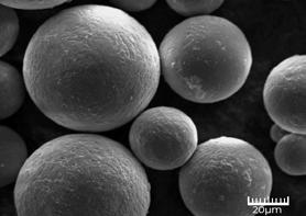
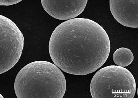
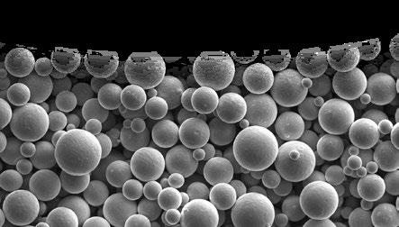
THE ART OF SPHERICAL POWDER
Aerospace
Cu-Alloys
CuCr1Zr
Ti-Alloys






Metal Additive Manufacturing | Spring 2024 29 Vol. 10 No. 1 © 2024 Inovar Communications Ltd | contents | news | events | advertisers | website | newsletter | GETPDF Industry News
Alloys developed and produced with EN 9100 certified quality
Ti64ELI / Ti5553 / TiCP
/ GRCop -42
HIGH QUALITY spherical and pore free metal powder for AM applications (LPBF, DED, ebeam,…)
part of UN Global Compact Initiative
Any metal or alloy based on www.metalpine.at
Bodycote completes Lake City takeover, ends Stack deal, announces £60M share buyback programme
Bodycote plc, headquartered in Macclesfield, Cheshire, UK, has, completed its previously announced acquisition of Lake City Heat Treating (HT), Warsaw, Indiana, USA. The company also announced that it had ended the agreement to acquire Stack Metallurgical Group, based in Albany, Oregon, due to a failure to satisfy all closing conditions to the agreement.
Lake City HT is a prominent Hot Isostatic Pressing (HIP) and vacuum heat treatment business, primarily supplying the orthopaedic implant market as well as civil aerospace. The move is expected to significantly increase Bodycote’s customer reach in the medical market.
The consideration paid on closing for Lake City HT was $66.5 million
on a cash and debt-free basis. After expected tax benefits worth approximately $7.5 million, the net price paid was $59 million. Lake City HT is forecasted to have achieved 2023 fullyear revenues of around $14 million, with operating profit expected to be around $6 million. The business achieved 30% revenue growth in 2023 and is expected to continue to deliver good progress.
“Completion of the acquisition of Lake City HT is an exciting further step in our strategy to grow our Specialist Technologies businesses and footprint,” stated Stephen Harris, Group Chief Executive of Bodycote plc. “This acquisition is an excellent fit, enhances our profitability and earnings per share in addition to allowing us to capitalise on the
appealing structural growth opportunities in medical and aerospace markets.”
£60 million share buyback programme
Bodycote also reported that, in light of the lower-than-anticipated acquisition spend, the group’s strong balance sheet and balanced approach to capital allocation, it has announced the intention to launch a share buyback programme of up to £60 million. The share buyback programme is expected to commence on March 18, 2024.
“The share buyback programme represents an attractive use of our capital,” Harris continued. “It highlights the strength of the group’s balance sheet, together with our commitment to a balanced and disciplined approach to capital allocation to drive growth and shareholder value.”
www.lakecityheattreating.com
www.bodycote.com

Metal Additive Manufacturing | Spring 2024 30 © 2024 Inovar Communications Ltd Vol. 10 No. 1 | contents | news | events | advertisers | website | newsletter | Industry News
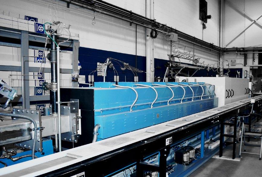
The furnaces have both debind and sinter capabilities 103 Dewey Street Bloomfield, NJ 07003-4237 | Tel: 973-338-6500 | Fax: 973-338-1625 www.cmfurnaces.com info@cmfurnaces.com Continuous high temperature pusher furnaces for high volume 3D printed metal parts
Lucideon partners with Naval Nuclear Laboratory to provide materials expertise
Lucideon, headquartered in Staffordshire, UK, is partnering with the US Naval Nuclear Laboratory (NNL) to help develop mission-critical technology to support component supply for the US Navy nuclear-powered fleet. Working with NNL in support of the Naval Nuclear Propulsion Program, Lucideon will contribute to research into the Hot Isostatic Pressing (HIP) process, which uses high pressure and elevated temperatures to densify materials.
From Lucideon’s two US sites – Greenville, South Carolina, and Schenectady, New York – the company will evaluate the thermal, physical, mechanical, and microstructural properties of a nickel-based superalloy, which has undergone the HIP process over a wide range of processing conditions.
Lucideon is a leading development and commercialisation organisation (DCO) with a global service portfolio, bringing together innovation and commercial knowledge. Its expertise spans the nuclear sector, in areas including new materials development and selection, comprehensive testing and analysis, and Additive Manufacturing support.
Lucideon’s work will be supported by its partner Dynamic Systems Incorporated (DSI), Austin, Texas, which has more than sixty years’ experience in the thermophysical simulations of materials. Complex evaluation of the material’s thermal diffusivity and expansion will be overseen from Lucideon’s base in the UK, working from the new high-technology AMRICC Centre. The project will be led by NNL’s Reactor Equipment Development unit, which is currently working to develop innovative manufacturing methods to enable new designs in support of the next generation of US Navy reactors.
“NNL is driving forward the development of this technology in an effort to supplement conventional forging for large, high-value, metallic components required within nuclear propulsion systems,” shared Tony Kinsella, CEO of Lucideon. “Increasing production volumes for submarines and surface ships are putting stress on existing supply chains, and this technology offers an opportunity to expand capacity and reduce the significant lead times that exist today. Under the twelve-month programme, we will be drawing on our world-leading material science testing and assurance capabilities, expertise, and technologies to enable and accelerate the R&D activity.”
“Ultimately this will provide the robust data NNL needs to fully characterise the PM-HIP process,” Kinsella added. “This is a highly complex project, which has the potential to deliver significant benefits to the US Navy nuclearpowered fleet.”
www.lucideon.com
www.amricc.com
Metal Additive Manufacturing | Spring 2024 31 Vol. 10 No. 1 © 2024 Inovar Communications Ltd | contents | news | events | advertisers | website | newsletter | GETPDF THE ART OF SPHERICAL POWDER HIGH QUALITY spherical and pore free metal powder for AM applications (LPBF, DED, ebeam,…) Any metal or alloy based on YOUR PARTNER FOR METAL POWDERS
Screening, classifying and packaging to our customers‘ needs
All processing steps possible under Argon 5.0 atmosphere
Standard PSDs for 5-20, 15-45, 20-63, 45106 µm
Specific PSDs for customized applications Customized to your needs Your benefits
Pure and uniform powders with 0% pores
High flowability
Lower oxygen content
Lower specific surface
Increased production rate www.metalpine.at part of UN Global Compact Initiative Industry News
•
•
•
•
•
•
•
•
•
Boeing funds Space Foundation’s new Additive Manufacturing Space Lab
Space Foundation, headquartered in Colorado Springs, Colorado, USA, has announced that Boeing has awarded the Space Foundation Discovery Center a grant to fund a new Additive Manufacturing Space Lab. Devoted to 3D design, manufacturing, and other AM and fabrication methods, the Boeing Additive Manufacturing Space Lab will be a new immersive education lab serving students, teachers and industry.
The Boeing Additive Manufacturing Space Lab aims to transform student learning, enhance visitor experiences, and foster global engagement through interactive digital activities and cutting-edge physical technology. Within the Lab, displays on the Additive Manufacturing industry will educate and inspire museum visitors, showcasing groundbreaking technology that has significantly impacted manufacturing and the space industry.
Space Foundation CEO Heather Pringle commented, “Boeing’s commitment to education aligns seamlessly with our mission, and we are immensely grateful for their continued support in propelling our Space

Boeing has awarded the Space Foundation Discovery Center a grant to fund a new AM Space Lab (Courtesy Space Foundation Discovery Center)
Foundation Discovery Center to the forefront of innovative educational offerings. This generous grant will fuel the creation of a new state-of-the-art Additive Manufacturing Space Lab, empowering educators, inspiring students, and connecting with partners worldwide. We are excited to continue this transformative partnership with Boeing, working hand in hand to inspire the next generation of space innovators.”



“The Space Domain is no longer the future of human discovery and national defence — it is the here and now, and students need the right skills to meet today’s moment,” stated Kay Sears, vice president and general manager of Boeing Space, Intelligence and Weapons Systems. “We are proud to support the Space Foundation’s new Additive Manufacturing lab at the Discovery Center in Colorado, which will serve as an important resource for students to learn through hands-on training and experience.”
Boeing has extensively utilised Additive Manufacturing in satellites, often surpassing traditionally-produced parts. With plans to advance AM in commercial, civil and government sectors, Boeing aims to be at the forefront of this technology for future crewed space missions. Recognising a shortage of skilled professionals in related fields, Boeing intends to partner with the Space Foundation to address this gap. Together, they will develop lab programming that targets students from the first grade onwards, with the goal of creating a diverse and inclusive learning environment that nurtures skills essential for AM careers.
The lab will integrate with other Discovery Center experiences, enhancing the overall learning environment. This synergy with existing labs, such as the Drone Lab and Lockheed Martin Mars Robotics Lab, amplifies the educational journey by leveraging AM technology. The lab fosters cross-disciplinary connections, promoting a comprehensive understanding of cutting-edge technologies. As the design and development phase continues, Space Foundation welcomes Boeing’s insights to optimise the lab’s components.
www.discoverspace.org
www.spacefoundation.org
www.boeing.com
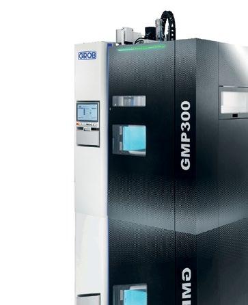
Metal Additive Manufacturing | Spring 2024 32 © 2024 Inovar Communications Ltd Vol. 10 No. 1 | contents | news | events | advertisers | website | newsletter | VISIT US! IN-HOUSE EXHIBITION April 16th – 19th ADDITIVE MANUFACTURING GROB METAL PRINTING Future-oriented, economical & flexible WANT TO KNOW MORE? CONTACT US AND VISIT OUR WEBSITE! www.grobgroup.com GROB_Anzeige_2024_Metal_AM_Additive_Manufacturing_91x120mm.indd 1 04.03.2024 11:07:30
Industry News


United States Metal Powders appoints Eric Degenfelder president
United States Metal Powders, Inc (USMP), Palmerton, Pennsylvania, USA, has announced the appointment of Eric Degenfelder as its president, effective February 2024. USMP, founded in 1918, is a global leader in the production of aluminium powder with two production facilities: AMPAL, Inc, also in Palmerton, and Poudres Hermillon, SARL (PH), in Hermillon, France. AMPAL has been operating in Palmerton for the last forty-two years, growing to be the largest US producer of aluminium powder. The company’s products are sold globally and used in a wide variety of end markets including aerospace & defence, automotive, industrial, consumer, building & construction and energy.
“We are very excited to have Eric join our team and welcome him to USMP,” said Louise Ramsey Thomas, board member and retiring president. “Eric brings a wealth of leadership experience in the specialty materials arena, and a strong track record of
enhancing growth through innovation, customer centricity and production excellence. We have great confidence in the USMP leadership team now in place and our ability to continue to deliver in a differentiated way for our customers. Over the last year, this team has also been enhanced with the additions of Danny Perez as General Manager of AMPAL, and Jean-René Cavaille as General Manager of PH.”
Degenfelder shared, “I am excited to join USMP and lead us into the next phase of growth. I have been highly impressed by the rest of the leadership team at AMPAL and PH, and was attracted to USMP’s strong market position, customer centric philosophy and the orientation toward continued investment and growth enabled by its fortress balance sheet and low financial risk profile. Rest assured we will continue our strong heritage of customer focus and quality in the years ahead.”
Degenfelder has leadership and cross-functional experience in
Jiangsu Vilory Advanced Materials Technology raises $50M for facility expansion
Jiangsu Vilory Advanced Materials Technology Co., Ltd (VMP), located in Jiangsu, China, has successfully raised $50 million in two rounds of financing. The funding will be used to finance the construction of VMP’s new production facility.
VMP offers a wide range of metal powders, produced using the company’s vacuum inert gas atomisation (VIGA) powder production technology. Currently, the company operates ten VIGA machines and has an annual capacity of 750 tonnes. It was stated that Phase II of the new facility is nearing completion and will soon be operational. Phase III of the development has now commenced.
The funding rounds were led by China State-owned Enterprise Mixed Ownership Reform Fund Co., Ltd., which became VMP’s second-largest strategic external shareholder. This was followed by Jiangsu State-owned Enterprise Mixed Ownership Reform Fund (Limited Partnership) and other Chinese institutions.
China’s Enterprise Mixed Ownership Reform Fund focuses on core technologies in key areas, striving to build a model for the reforming of state-owned science and technology enterprises and pioneering independent innovation. Its investment in VMP is expected to further strengthen the

Eric Degenfelder has been named
United States Metal Powders President (Courtesy Eric Degenfelder/ LinkedIn)
specialty materials. He was CEO of U-C Coatings, headquartered in Buffalo, New York, for the past four years, and prior to that held a series of functional and geographic roles of increasing responsibility spanning product management, sales, marketing and strategy for Axalta Coating Systems, DuPont, Air Products and Millennium Chemicals. He received his BS in chemical engineering from Cornell University, and an MBA from Kellogg School of Management.
www.usmetalpowders.com
company’s position in the industry, and promote the development of metals for the Additive Manufacturing sector.
Jiangsu Mixed Reform added that its investment is intended to help VMP strengthen its research and development capabilities, expand production capacity and serve the country’s manufacturing strategy.
During 2023, VMP undertook two national key R&D projects and reported new breakthroughs in the research and development of five materials. The company also developed what is reputed to be the country’s first single-furnace VIGA equipment with a charging capacity of 500 kg, which has now been put into production. Throughout the year, twenty-six invention patents were authorised, resulting in a total of 143 patents now authorised.
www.wllxcl.com
Metal Additive Manufacturing | Spring 2024 34 © 2024 Inovar Communications Ltd Vol. 10 No. 1 | contents | news | events | advertisers | website | newsletter | Industry News
3D Printing Guide for Dental Technology
Find the right TruPrint machine for your application!

Are you searching for the right machine for your applications in dental technology? Find the perfect solution with our intuitive Product Finder, guiding you through the exceptional capabilities of the TRUMPF TruPrint 1000 and TruPrint 2000 Take advantage of our special offer until May 31st 2024: Receive the Preform or Multiplate option for free when purchasing your new TruPrint 1000!
More information at http://www.trumpf.com/s/truprint-productfinder

SPECIAL OFFER
AddUp appoints Nick Estock as Deputy CEO for North America
AddUp Inc., headquartered in Cébazat, France, has appointed Nick Estock as its Deputy Chief Executive Officer for North America, succeeding Rush LaSelle.
Estock has over fifteen years in the manufacturing industry across multiple Additive Manufacturing technologies. With AddUp since 2021, the company has said that Estock emphasises a relentless commitment to driving customer success and embracing cutting-edge technologies.
“I am honoured to take the role of Deputy CEO for AddUp North America,” Estock stated. “Additive technology is not just a profession for me, it is a passion that drives me to push the boundaries of what’s possible. I am proud to be at the forefront of this technology built on the 200+ years of industrial experience of Michelin and Fives.”
“I feel privileged to lead our team in Cincinnati [Ohio]. I have witnessed this group deliver time and time again real industrial solutions to our customers’ most difficult challenges and I look forward to fostering our customer-first culture,” he concluded.
Estock has a background in design, product development, and new product introduction and found success early on in his career with companies like GE Additive, Case New Holland and BAE Systems. Prior to joining AddUp, Estock held several leadership roles within GE Additive culminating in the Program Leader for its metal Binder Jetting (BJT) development where he oversaw the first production parts off the company’s BJT machine.
“Nick brings with him a deep and intimate understanding of our

customers’ unique challenges for the US Market,” explained Julien Marcilly, CEO of AddUp. “His passion for manufacturing excellence and dedication to customer satisfaction align seamlessly with the company’s core values, setting the stage for an exciting chapter of growth and innovation.”
www.addupsolutions.com

| contents | news | events | advertisers | website | newsletter | Industry News
Nick Estock has been named AddUp’s Deputy CEO of North America (Courtesy AddUp)

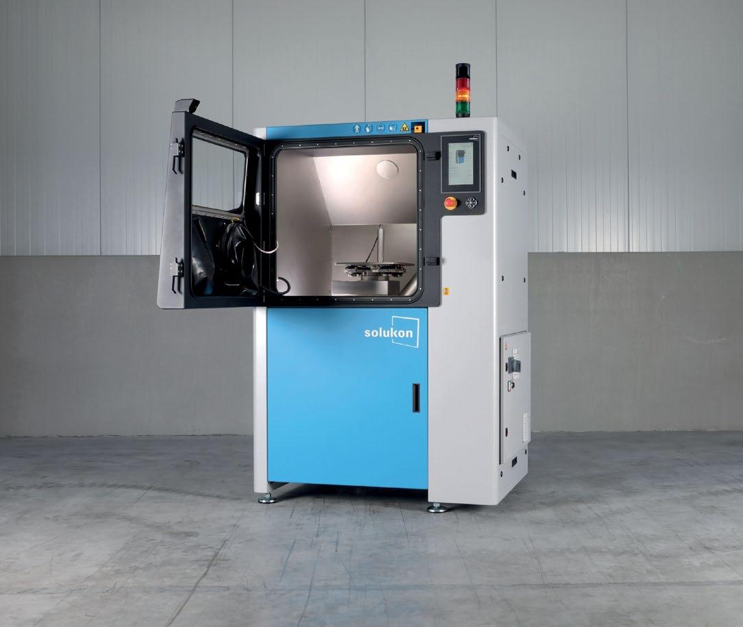
For delicate structures
SFM-AT350-E with piezoelectric excitation in ultrasonic range
NEW
self-regulating excitation
avoiding harmful vibrations
silent process
minimized compressed air consumption
solukon.de
NEW
Zeda’s acquisition of Orthopaedic Implant Company to expand options for Additive Manufacturing in medical sector
Zeda, Inc, Fremont, California, USA, has acquired the Orthopaedic Implant Company (OIC), based in Reno, Nevada. The move will enable Zeda to produce OIC’s implant designs in an effort to fortify and accelerate its goal of providing accessible, high-value trauma implants to patients on a worldwide scale.
“The acquisition of OIC represents a pivotal moment for Zeda,” stated Shri Shetty, CEO of Zeda. “Its leadership in value-based implants perfectly complements our Additive Manufacturing technologies that can deliver high-quality orthopaedic devices and implants that are accessible to all patients, regardless of country and socioeconomic
status. Together, our strengths and expertise will raise the standard of care globally and equitably for the world’s entire population.”
Itai Nemovicher, CEO and co-founder of The Orthopaedic Implant Company, added, “We are proud to join forces with Zeda, a company that shares in our values and dedication to advancing access to critical orthopaedic care because it can and should be done. Under Zeda, OIC will reach new heights in providing cost-effective, high-quality orthopaedic solutions in the US and abroad.”
Under the terms of the acquisition by Zeda, OIC will operate worldwide as a Zeda Health company. The deal is intended to
solidify Zeda’s position in the global orthopaedic industry as a company developing and using leading design and manufacturing technologies that push device design forward whilst improving affordability and access to care.
www.orthoimplantcompany.com www.z8a.com

Metal Additive Manufacturing | Spring 2024 38 © 2024 Inovar Communications Ltd Vol. 10 No. 1 | contents | news | events | advertisers | website | newsletter | Industry News
Aluminum Alloy Powders for Additive Manufacturing
Zeda uses metal Additive Manufacturing to produce a range of medical implants (Courtesy Zeda Inc)
Ursa Major tipped to supply additively manufactured rocket motors to Pentagon
Ursa Major Technologies Inc, located in Berthoud, Colorado, USA, is close to receiving a contract to produce solid fuel rocket motors for the Pentagon, reports Reuters.
US officials are said to be seeking suppliers beyond the two dominant rocket engine makers, Northrop Grumman and L3 Harris Technologies, as it looks to meet missile and rocket orders to supply the war efforts in Ukraine and Israel, and to re-stock dwindling US inventories.
The contract, although expected to be relatively small and fall under the Pentagon’s development programmes, would be seen as a big vote of confidence in Ursa Major and its metal Additive Manufacturing technology.
“As soon as I get the FY (fiscal year) ’24 budget, I am going to drop it on a small company that is going to do Additive Manufacturing of a solid rocket motor,” Heidi Shyu, under secretary of defence for research and engineering, told Congress last week. “We can’t wait to get them on contract.”
While Shyu did not name the company or reveal the size of the contract during her testimony, she did say that the company had been working closely with the Navy. A congressional aide and an industry executive who spoke on condition of anonymity reportedly said Shyu was referring to Ursa Major.
An industry executive from a large defence prime contractor said Ursa Major’s motors can be used in any small diameter weapons like the new Boeing and SAAB Ground Launched Small Diameter Bomb (GLSDB), RTX’s SM-6 rockets and Lockheed Martin’s Guided Multiple Launch Rocket System (GMLRS) which are used heavily in Ukraine.
www.ursamajor.com
Desktop Metal files prospectus for mixed shelf offering up to $250M
Desktop Metal, Inc, headquartered in Burlington, Massachusetts, USA, has filed a prospectus for a mixed securities shelf offering up to $250 million.
The prospectus was submitted on February 14, 2024, in a Securities and Exchange Commission (SEC) Form S-3 filing. The mixed shelf offering
includes a range of securities, such as preferred stock, debt securities, warrants, units and up to $75 million of class A common stock.
The offering follows Desktop Metal’s announcement of a $50 million savings plan in January of this year.
www.desktopmetal.com
Metal Additive Manufacturing | Spring 2024 39 Vol. 10 No. 1 © 2024 Inovar Communications Ltd | contents | news | events | advertisers | website | newsletter | GETPDF Industry News
Freemelt collaborates with Weaream to bring eMELT Additive
BESPOKE MACHINES

Manufacturing to Italian industry
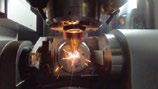
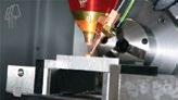
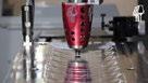
Freemelt AB, Mölndal, Sweden, has entered a strategic collaboration with Weaream, an Additive Manufacturing service provider based in Brescia, Lombardia, Italy. Together, the companies aim to use Freemelt’s eMELT Electron Beam Powder Bed Fusion (PBF-EB) Additive Manufacturing machines for serial production.
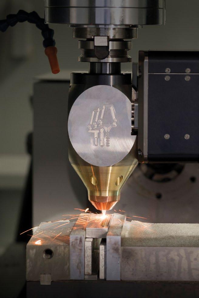
”Freemelt and Weaream are a perfect match! It is exactly this kind of strategic collaboration the manufacturing industry needs and embraces – competence and application centres supporting industrial companies in the transition to more innovative manufacturing technology, like 3D printing,” stated Daniel Gidlund, Freemelt CEO. “This strategic partnership ensures that eMELT and the E-PBF technology (Electron Powder Bed Fusion) take another important step in establishing Freemelt and eMELT as the leading technology for innovative serial production of industrial applications.”
Industrial companies that are transitioning from traditional manufacturing to Additive Manufacturing can experience a significant gap in competence and support in application and product development, it was stated. This gap needs to be bridged to ensure an efficient transition to serial production with Additive Manufacturing, which is essential when moving towards a more innovative, cost-effective, and sustainable manufacturing sector.
Paolo Folgarait, Weaream CEO, added, ”With this strategic partnership, Weaream and Freemelt will enable the full
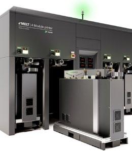
potential by complementing each other perfectly to serve the market, support clients and the industry to adopt high-tech solutions based on new materials and the most innovative Additive Manufacturing technologies. Weaream is proud and excited about this collaboration with Freemelt.”
The Italian AM industry has been experiencing steady growth of approximately 20% over the past decade. The northern region has for many years been a cluster of key early adopters and innovative companies in research, design, and engineering, which have been driving the industrialisation of AM. The Italian State and the European Union are said to be strong drivers behind the successful development of Additive Manufacturing in Italy, providing funding and resources.
Maurizio Romeo, Weaream CTO, concluded, “Thanks to our long-term expertise in E-PBF technology, Weaream is a perfect partner for Freemelt to ensure that the eMELT technology will deliver effective industrial production of demanding applications, where new materials and cutting-edge technologies will make the difference.”
www.freemelt.com
www.weaream.it
© 2024 Inovar Communications Ltd Vol. 10 No. 1 | contents | news | events | advertisers | website | newsletter | Industry News ADDITIVE SUBTRACTIVE INSPECTION
INNOVATING
START
TODAY
AND VERSATILITY WWW.HYBRIDMANUTECH.COM
FLEX20
EFFICIENCY
AMBIT™
AMBIT™FLEX20 AMBIT™MULTI20WIRE AMBIT™WAVE AMBIT™ONE10 AMBIT™XTRUDE
The eMELT-iM is an Electron Beam Powder Bed Fusion Additive Manufacturing machine for serial production (Courtesy Freemelt AB)
USING ARGON OR NITROGEN?
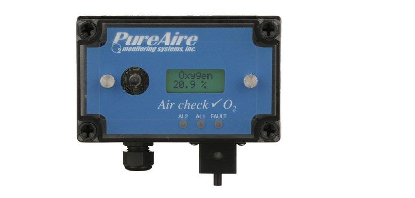
THE OXYGEN SAFETY SOLUTION
Inert gases displace oxygen, creating an oxygen-deficient environment ideal for printing processes but not for personnel safety. Oxygen deficiency monitors contribute to safe working environments in any applications utilizing oxygen-depleting gases.
• Long-Life 10+ Average Sensor Life
• Measures 0-25% Oxygen
• Continuously Measures Inert Gases Including Argon and Nitrogen
• Operating Temperatures -40º to 140ºF (-40º to 60ºC)
• No Scheduled Maintenance
• Plug and Play Set-Up
• Built-In 90dB Horn

wwww .P ureAireMonitoring.com
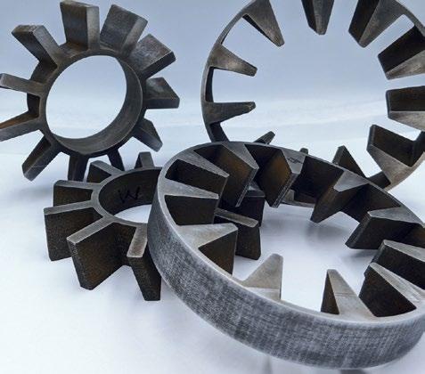
Steel Powder for Additive Manufacturing
Water Atomized Low Carbon and Low Alloy Steel
Low-Cost Solution for Industrial AM Applications
• Laser Powder Bed Fusion
• Powder Bed Binder Jetting
• Direct Energy Deposition
• Cold Spray Additive Manufacturing
• E-Beam Additive Manufacturing
Authentise secures three grants in support of its Open Innovation initiatives
Authentise has announced it has been awarded three grants in support of its Open Innovation initiatives. Supported by Innovate UK, the US Department of Energy and Eureka, the projects look to drive Additive Manufacturing applications and make the process more secure and efficient.
“These grants show that Authentise keeps pushing the boundaries of Additive Manufacturing to help accelerate the technology benefits of our customers: AM power users,” stated Erica Vlahinos, VP of Additive Manufacturing at Authentise. ”Together, we are delivering a more secure and efficient technology, ready to penetrate further into the heart of manufacturing as a whole.”
Simon McCaldin, VP Open Innovation at Authentise, added, “Authentise has always pursued a very intentional open innovation approach working with a myriad of partners around the world to address some of the industry’s most pressing challenges. We’re delighted to have been trusted by both our project and funding partners to provide the digital backbone of the solutions. We’re excited to share the progress of these and many other projects to come.”
The grants include
METAMAT: Lattice structures are a key value driver for AM, but manufacturing challenges remain. Together with NS85, Teesside University, Lancaster University, and Holdson, Authentise aim to overcome these challenges and ensure highly-functional metallic lattice parts at scale. Authentise’s role in the project is to develop a seamless integration between manufacturer, designer and customer.
DISTOPIA: Together with EPOCH, AMRC, Queen Mary University London, ION Metal, and Turkish Aerospace, Authentise aims to develop a seamless, ready-to-use plasma-based Directed Energy Deposition solution that addresses the needs of the manufacturing, repair, and remanufacturing sectors, especially in aerospace. Authentise will use its expertise in data-driven workflow management and digital manufacturing methods with state-of-the-art material technology.

AM-Verify: Authentise is one of ten selected for funding by the US Department of Energy through the Cybersecurity Manufacturing Innovation Institute (CyManII). The project aims to build a secure real-time measurement system specifically to detect if malicious third parties have infiltrated an AM system. Authentise, I3D MFG, and Addiguru will demonstrate multiple verification data streams, all integrated into the CyManIIdeveloped Cyber-Physical Passport.
www.authentise.com
Metal Additive Manufacturing | Spring 2024 42 © 2024 Inovar Communications Ltd Vol. 10 No. 1 | contents | news | events | advertisers | website | newsletter | Industry News
IATF 16949 ISO 9001
Specialty Grades - Composition (wt%) Grade C Mn Mo Cr Ni Si ATOMET 0.20-0.35 0.70-0.90 - - - 0.10-0.25 1025 ATOMET 0.38-0.43 0.60-0.80 0.20-0.30 0.70-0.90 1.60-2.00 0.10-0.25 4340 ATOMET 0.55-0.60 0.15-0.20 0.80-0.90 - -4405 Find out more
AM
qualloy launches online metal powder marketplace for Additive Manufacturing
A new online metal powder marketplace has been established by qualloy, a Düsseldorf, Germany-based intermediary for buyers and sellers in the metal powder market. The platform is designed to transform the way businesses procure metal powders for Additive Manufacturing and related applications by providing full transparency on prices and delivery terms. It is expected to enable users make informed decisions quickly.
“Our team at qualloy is dedicated to driving innovation in the Additive Manufacturing industry,” stated Yannik Wilkens, co-founder of qualloy. “With the launch of our marketplace, we are empowering businesses to access a diverse range of high-quality metal powders with ease and efficiency.”
The qualloy marketplace offers a range of features designed to enhance the sourcing experience for users, including advanced search algorithms, transparent pricing, and detailed product specifications. Additionally, qualloy’s team is on hand to provide guidance and support throughout the procurement process.
The marketplace will connect customers with globally-certified powder suppliers by way of a variety of filtering options, including application, base material, atomisation process, and particle size distribution. This is intended to allow users to find the most suitable metal powder for their requirements with ease. As soon as powders are in the shopping basket, the purchase can be confirmed with one click. The marketplace’s interface and clear

qualloy has launched its online metal powder marketplace (Courtesy qualloy)
categorisation of products is an effort to simplify navigation, making the sourcing process effortless.
“We believe that our marketplace will not only simplify metal powder sourcing but also accelerate the adoption of Additive Manufacturing technologies,” added Wilkens.
www.qualloy.com
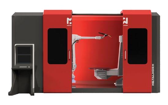
Multi-purpose use:
Metal Additive Manufacturing | Spring 2024 43 Vol. 10 No. 1 © 2024 Inovar Communications Ltd | contents | news | events | advertisers | website | newsletter | GETPDF Industry News Real-time monitoring of the entire system and offers a unique digital twin solution. Complete solution for flexible and user friendly offline robotic tool path planning software Non limited manufacturing with Special Robotic WAAM system Allows for printing parts that are dozens of meterslong and weigh tons. Customized robotic system configurations are available.
WAAM, Repair and Welding
Wire Arc Additive Manufacturing System
Robotic
Oechsler Group announces restructuring with centralised production and management
The Oechsler Group, headquartered in Ansbach, Germany, has announced it is reorganising its group structure into three business units with a central production responsibility. Under the internally-named BE:FOCUSED programme, Oechsler is aiming to streamline structures, simplify the organisation, and centralise operations.
It was stated that evolving demands in tasks and job roles will result in the creation of new positions as well as job reductions. Globally, approximately 220 positions are impacted by the job cuts, with around 135 in Germany.
A structure with three divisions and centralised production
The new corporate structure will focus on three business units (BU) aligning with the company’s strategic market opportunities: Mobility, Innovative Solutions, and Health.
Oechsler has decided to discontinue its Sporting Goods business and will
only engage in sales in China in this sector if favourable opportunities arise. China will serve as a supplier base for multinational clients in the region. Enhanced collaboration with Chinese toolmakers and utilising their production capacities will enhance efficiency and optimise the product range for customers. Additionally, adjustments are expected in the realm of Additive Manufacturing, it was stated.
Oechsler will centralise worldwide production and its management in one location. The plants within the global group will focus on enhancing production efficiency. Sales responsibilities for regions and countries where Oechsler operates will now be coordinated centrally at the company’s headquarters in Ansbach, rather than being managed locally at the plants. The three German locations of Oechsler will reportedly continue to play a significant role.
“With BE:FOCUSED, we are launching an extensive investment
Additive Plus to market Farsoon’s industrial Additive Manufacturing solutions to the West Coast US
Farsoon Americas, the US-based division of Farsoon Technologies, headquartered in Hunan, China, has announced a distribution agreement with Additive Plus, based in Torrance, California. Through this partnership, Additive Plus will market Farsoon’s industrial-grade metal and plastic Additive Manufacturing machines to the American West Coast.
Additive Plus delivers AM hardware and technical solutions targeting series production that span various industries, including automotive, dental, healthcare, education, and beyond.
“Given that Additive Manufacturing and laboratory atomisation technolo -
gies are our core offerings, we’ve learned from our clients that the ability to work with custom and traditional materials is a game changer,” stated Harry B Saltos, Business Development Manager of Additive Plus.
“Access to an open system providing full laser control is the emerging trend in both industry and academia. Farsoon offers the freedom to work with any material and control all printing parameters, making it the key to next-generation manufacturing,” added Saltos.
Don Xu, Managing Director of Farsoon Americas, added, “I am excited to partner with Additive
programme for our successful future. Over the past few months, we have analysed very intensively how we can return to a profitable growth path in the long term. We too have been navigating increasingly stormy waters for several years due to changing market conditions, geopolitical changes and increased competitive pressure from our customers. For this reason, we will reorganise ourselves and set the right course again with BE:FOCUSED,” stated Karl Ostler, CEO of Oechsler AG.
“We understand that ultimately, it’s about people and not just ‘jobs.’ Therefore, we will proceed with caution,” added Ostler. “Unfortunately, some colleagues will have to leave the company. We shared our plans with the General Works Council early on and in a transparent manner. I want to express my gratitude to our works council members for their positive discussions. They have passionately represented our employees’ interests and acknowledged the necessity for action. This has allowed us to achieve an agreement and promptly provide clarity for our colleagues.”
www.oechsler.com
Plus to bring the latest Farsoon’s laser powder bed technology to the western US market. With their strong knowhow in a variety of manufacturing technologies, Additive Plus will be a valuable resource for customers and Farsoon.”
www.additiveplus.com
www.farsoon-gl.com
Metal Additive Manufacturing | Spring 2024 44 © 2024 Inovar Communications Ltd Vol. 10 No. 1 | contents | news | events | advertisers | website | newsletter | Industry News
From left: Harry B Saltos, Business Development Manager at Additive Plus; Don Xu, Managing Director of Farsoon Americas; Ashkhen Ovsepyan, CEO of Additive Plus (Courtesy Farsoon Technologies)
TANIOBIS
Based on our 60 years expertise in manufacturing and development of refractory metals, we have developed AMtrinsic® atomized tantalum and niobium spherical powders and their alloys for demanding additive manufacturing technologies. Our ability to adjust specific intrinsic material properties enables us to push the limits according to the requirements of your application.

AMtrinsic® spherical tantalum and niobium powders provide outstanding combinations of material properties customized for specific applications. Aligned with 3D-printing technology, AMtrinsic® powders can help overcome hurdles in various high-tech industries. The high temperature stability, excellent corrosion resistance and biocompatibility of AMtrinsic® Ta, Nb powders and their alloys deliver a perfect fit for biomedical (Ta, TNT and TNTZ), chemical (Ta, Nb, Ta-W) and aerospace (Ta-W, C103 and FS-85) applications. In addition, AMtrinsic® Nb with its prominent superconducting properties is ideal for the superconducting industry.
and
1Zr) pre-alloyed powders. Hightemperature strength, superior creep properties and their excellent workability with Additive Manufacturing make these alloys great candidates as structural materials for various aerospace applications. AM offers design freedom enabling manufacturing of lightweight components with complex features e.g. rocket thruster with integrated cooling channels which is one of the many applications of our AMtrinsic® C103 and FS-85 alloys.

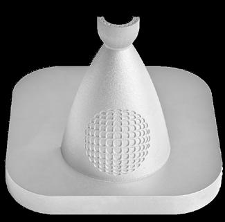
 TANIOBIS offers atomized AMtrinsic® C103 (Nb-10Hf-1Ti)
FS-85 (Nb-28Ta-10W-
HEA
Ti-Nb-Ta
Ta-W
FS-85
C103
TANIOBIS offers atomized AMtrinsic® C103 (Nb-10Hf-1Ti)
FS-85 (Nb-28Ta-10W-
HEA
Ti-Nb-Ta
Ta-W
FS-85
C103
108.95 73
TNTZ Ta
92.906 41
Nb
Prototal Industries acquires Additive Manufacturing specialist CA Models in UK expansion strategy
Prototal Industries, headquartered in Jönköping, Sweden, has recently acquired CA Models, an Additive Manufacturing specialist based in Stirling, Scotland. The deal is said to mark a significant milestone in Prototal Industries’ growth strategy, demonstrating its commitment to expanding its presence and offerings in the UK. The addition of CA Models to the group looks to add expert competence and capacity to the already established Prototal UK operations, located in Newbury, England.
“We are thrilled to welcome CA Models into Prototal Industries. This strategic move aligns with our vision for growth and innovation and will strengthen our capabilities for production volumes with
Additive Manufacturing. We are confident that the integration of our teams will be successful and further strengthen our position as the preferred production partner in Europe and the UK,” shared Jan Löfving, CEO, Prototal Industries.
The acquisition of CA Models brings complementary strengths, expertise, and capabilities to Prototal Industries. As a result, Prototal can now offer a broader range of services and solutions, including metal Additive Manufacturing, five-axis CNC machining, CNC turning, EDM wire erosion, CMM inspection, 3D scanning and a vast range of polymer Additive Manufacturing, such as SLA and SLS, requiring highly intricate model-making skills.
Gregory Campbell, Operations Director of CA Models stated, “We are delighted to join the Prototal Industries family and are excited to contribute our skills and expertise to expand on the wide range of technology the group already has. With our strong experience in metal Additive Manufacturing and precision CNC machining, Prototal Industries can now offer its customers an even wider range of component manufacturing solutions.”
The acquisition was completed on February 1, 2024, and Prototal Industries and CA Models are now working to ensure a smooth and effective integration of the new team. Collectively, CA Models and the Prototal UK team aim to expand its market presence, enabling Prototal to reach a wider audience and serve customers more effectively and efficiently across the UK. www.prototalindustries.com www.camodels.co.uk

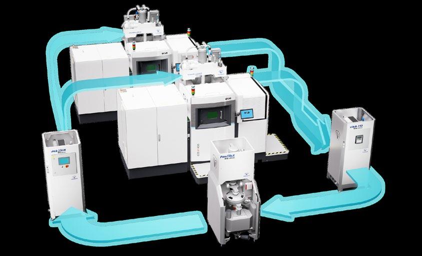
Metal Additive Manufacturing | Spring 2024 46 © 2024 Inovar Communications Ltd Vol. 10 No. 1 | contents | news | events | advertisers | website | newsletter | Industry News
Acerinox to invest €67 million in VDM Metals, boosting powder production
Acerinox Group, Madrid, Spain, has announced plans to invest €67 million in VDM Metals, its high-performance alloys (HPA) division. The funds will be allocated to German facilities in Unna, Altena and Werdohl, with three new remelting units and a second powder atomisation plant being built at the Unna site.
VDM Metals produces nickel alloys and high-alloy special stainless steels in sheet, strip, bar, wire and powder form. The investment will enable the company to expand production capacity across its range of products.
VDM has represented the Acerinox’s HPA division since March 2020. In 2022, VDM Metals achieved a turnover of €1.262 billion and a record EBITDA of €125 million; finished goods production amounted to 44,000 tonnes. VDM Metals employs over 2,000 people worldwide, around 1,600 of whom work at the Unna, Altena and Werdohl sites.
www.vdm-metals.com
www.acerinox.com
Laboratory Testing Inc invests $3M to expand fatigue testing lab
Laboratory Testing Inc. (LTI), Hatfield, Pennsylvania, USA, has invested over $3 million to install sixteen new fatigue testing frames at its facility, bringing the total it now has in the lab to fifty-two. This expansion aims to meet the increasing demand it is witnessing for comprehensive materials testing services, particularly in the aerospace, space, defence and Additive Manufacturing sectors.
Fatigue testing is a critical method for assessing material performance under various conditions, ensuring the reliability and durability of components in mission-critical projects. LTI’s enhanced capabilities will enable engineers and technicians to conduct strain-controlled fatigue testing across a spectrum of temperatures.
Brandon McVaugh, LTI President, shared, “We are thrilled to enhance our support for clients in the aerospace, space, defence, and Additive Manufacturing sectors through the expansion of our fatigue testing lab. This investment underscores our commitment to providing high-quality, advanced testing solutions to meet the evolving needs of our mission critical customers. As the industry experiences an upturn in the coming years, LTI will continue to lead by developing capacity, investing in expanding technologies, and furthering our capabilities to support the progression of the industry.”
LTI offers a range of complex testing procedures, including metal powder characterisation, non-destructive testing, crack propagation, high cycle fatigue, and low cycle fatigue testing.
www.labtesting.com
Metal Additive Manufacturing | Spring 2024 47 Vol. 10 No. 1 © 2024 Inovar Communications Ltd | contents | news | events | advertisers | website | newsletter | GETPDF Industry News
IperionX’s commercial-scale titanium production on schedule
IperionX Limited, based in Charlotte, North Carolina, USA, has announced that its titanium furnace has completed final mechanical assembly and successfully passed factory acceptance tests with the IPX technical team. The Hydrogen Assisted Metallothermic Reduction (HAMR) titanium industrial furnace is now being transported to the US, with anticipated delivery to the Titanium Manufacturing Campus during the first quarter of 2024.
Installation and commissioning of the HAMR titanium furnace is expected during the second quarter before producing the first titanium metal in mid-year 2024.
Named a critical IperionX production asset, this large-scale, industrial titanium furnace leverages patented company technologies – such as HAMR1 and HSPT2 – to produce sustainable, high-strength titanium metal products at commercial scale.
The application of this conventional furnace technology for titanium production has undergone a comprehensive furnace test work programme. In 2023, the IperionX technical team successfully completed two full-scale titanium production test runs that reportedly
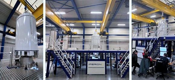
surpassed the core target production parameters for the Titanium Production Facility.
Construction progress
Construction of the Titanium Production Facility is advancing to schedule, with the construction of the Advanced Manufacturing Center also on schedule and anticipated to be commissioned during the second quarter of 2024.
Further, IperionX has received the first $2.4 million payment from the $12.7 million US Department of Defense DPA Title III grant to fund Phase I ramp-up of its Virginia Titanium Production Facility, comprising the Titanium Production Facility and the Advanced Manufacturing Center.

This advanced manufacturing unit will utilise angular and spherical titanium powders from the Titanium Production Facility to manufacture a wide range of low-cost and high-performance titanium products using Powder Metallurgy, Hydrogen Sintering & Phase Transformation (HSPT) forging and Additive Manufacturing. It will also leverage CNC machining, post-processing equipment and advanced R&D laboratories to support customer and government engagement.
“IperionX is nearing an important milestone designed to revitalise the US titanium supply chain with a unique end-to-end solution that spans from recycled scrap titanium to high-performance forged titanium products,” stated Anastasios (Taso) Arima, IperionX CEO. “Our patented titanium technologies can produce a wide range of high-performance titanium products – including angular and spherical titanium powders, semi-finished titanium products, near-net titanium shape products and additively manufactured titanium components – with superior energy efficiency, lower costs, and lower environmental impacts.”
“We have a strong pipeline of potential US government funding and incentive programmes designed to re-shore and secure critical mineral and metal supply chains. The commissioning of our Virginia Titanium Manufacturing Campus will be a pivotal step forward, positioning IperionX with an innovative end-to-end titanium supply chain capable of manufacturing high-performance and low-cost titanium products for advanced American industries.”
www.iperionx.com
Metal Additive Manufacturing | Spring 2024 48 © 2024 Inovar Communications Ltd Vol. 10 No. 1 | contents | news | events | advertisers | website | newsletter | Industry News
IperionX’s HAMR furnace in the Titanium Production Facility (Courtesy IperionX)
ILLUMINATING
ALL THINGS AM

IN THE COMPLEX LANDSCAPE OF AM, LET LUCIDEON BE YOUR GUIDING LIGHT
PARTNER WITH US AND UNLOCK A PATHWAY TO STREAMLINED SOLUTIONS, INNOVATIVE PROCESSES, AND UNPARALLELED SUPPORT IN AM
• Gain priority access and a partnership style approach with our tailored solutions
• We s treamline processes for swift turnarounds while ensuring accountability and transparency
• Ben efit from industry-leading technical support and partnerships on validation and qualification
• Our c onsultative approach offers exclusive client treatment, enhanced customer service, and cross-material expertise
• Colla borate with us for supplier benchmarking, equipment validation, process optimization, and more
CONTACT US NOW AND WE’LL HELP YOU REACH NEW HEIGHTS...

query@lucideon.com
www.linkedin.com/company/lucideon
www.lucideon.com
ADDITIVE MANUFACTURING SOLUTIONS (LAMS)
EOS extends range with EOS M 290 1kW metal Additive Manufacturing machine
EOS GmbH, headquartered in Krailling, Germany, has expanded its EOS M 290 range with the new EOS M 290 1kW, specifically designed for copper and copper alloy additively manufactured applications. At launch, the Laser Beam Powder Bed Fusion (PBF-LB) metal Additive Manufacturing machine is fully qualified to process EOS copper CuCp and EOS copper CuCrZr, with
additional materials expected to be added to the machine compatibility portfolio later in 2024.
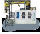



“Our award-winning EOS M 290 is one of the most widely used metal AM machines in the world, and now the family is growing. Interestingly, the EOS M 290 1kW was developed by EOS’ AMCM group as part of its custom AM portfolio. The call to further commercialise this platform was exceptionally strong due to market demand, so now we are slip-streaming it into EOS’ broader portfolio,” shared Monica Smith, EOS metal product line manager.
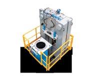
The new EOS M 290 1kW is specifically designed for copper and copper alloy additively manufactured applications (Courtesy EOS)

The EOS M 290 1kW was developed by EOS’ AMCM group to support the design and manufacturing of copper inductor applications and is ideal for a wide range of industries, including space, energy, and mobility/ transportation.
The new Additive Manufacturing machine features a build volume of 250 x 250 x 325 mm and includes a 1,000 W laser. It has a build volume rate of up to 55.4 mm³/h and a scanning speed of up to 7.0 m/s. The focus diameter of the EOS M 290 1kW is approximately 90 µm.
One early adopter of the technology was GBZ Mannheim GmbH & Co.KG, a specialised manufacturer of inductors and other highly engineered components for the automotive industry.
“Additive Manufacturing and the new one-kilowatt technology allow us to design and manufacture copper inductor applications that are more capable, durable and now produced in one piece with no soldering points,” said Thomas Corell, managing director at GBZ Mannheim. “The core elements of inductor applications are now integrated in a single build, and the results are much higher optimisation of the cooling channels, lower power consumption during the product lifecycle, and we are seeing great reproducibility on the production side of things.”
www.eos.info
Metal Additive Manufacturing | Spring 2024 50 © 2024 Inovar Communications Ltd Vol. 10 No. 1 | contents | news | events | advertisers | website | newsletter | Industry News HOT & COLD ISOSTATIC PRESSES MANUFACTURERS Equipment for metal and ceramic components post-processing TECHNOLOGY MANUFACTURERS Efficient Production Improved Properties Cost Reduction 100% Theorical Density DISCOVER OUR INDUSTRIAL PRESSES Wire wound vessel Robust yoke design Compressorsmade in house Fast cooling capabilities www. hiperbaric.com GLOBAL LEADER IN HIGH PRESSURE TECHNOLOGIES Visit us & try your products at our HIP INNOVATION CENTER Hiperbaric factory in Spain Meet us at Booth 838 C M Y CM MY CY CMY K
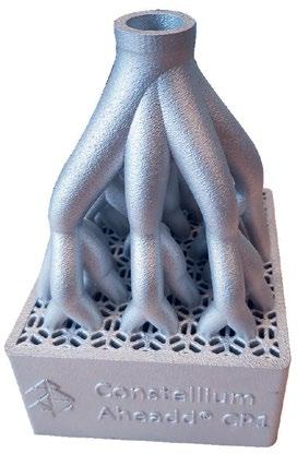
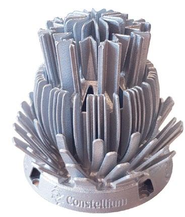
Aheadd® Aluminium powders Specifically designed and optimized for Additive Manufacturing Aheadd® CP1 High conductivity & productivity Aheadd® HT1 High temperature & strength The solution of choice for: n Aerospace n Automotive/Motorsport n Defense n Transportation n Semiconductor Courtesy Volum-e, designed by Gen3d Courtesy GMP Expanding the boundaries of your application Aheadd® aheadd@constellium.com
Incus is expanding its material portfolio with 99.9% pure copper
Incus GmbH, based in Vienna, Austria, is expanding its material portfolio with the progression of 99.9% pure copper material to the production stage. While it has closely collaborated with external partners on copper development, Incus has now initiated its internal R&D activities.
Incus has been focusing on improving the binder system of its lithography-based metal manufacturing (LMM) – defined as a vat photopolymerisation process (VPP) by ISO/ASTM – for nearly a year. After conducting the first furnace runs, Incus was able to achieve isotropic 92% of the electrical and thermal conductivity of conventionally produced copper. Furthermore, the total time spent in the sintering furnace was optimised below twelve hours.
Oxygen-free copper is used in various applications, such as thermal management systems, electrical connectors, and RF communication. Using LMM, Incus can additively manufacture copper pieces with unparalleled surface aesthetics and the highest geometrical complexity. LMM’s strength lies in its ability to eliminate the need for support structures during the manufacturing process, ensuring a homogenous powder distribution free of any defects and the best possible material performance.
The Incus technology offers a high solid loading of up to 60Vol.% of copper powder, enabling the highest density and optimal shape post-sintering. High solid loading is key to achieving the best mechanical properties and preventing deformation during sintering.
Incus is expanding its material portfolio with 99.9% pure copper material (Courtesy Incus)
Incus has been able to reach such high solid loadings in LMM due to the combination of the binder system and its recoating mechanism. This enables consistent part homogeneity and quality, regardless of part volume. With one parameter set, Incus can manufacture both smaller complex parts and larger volume parts simultaneously.
www.incus3d.com
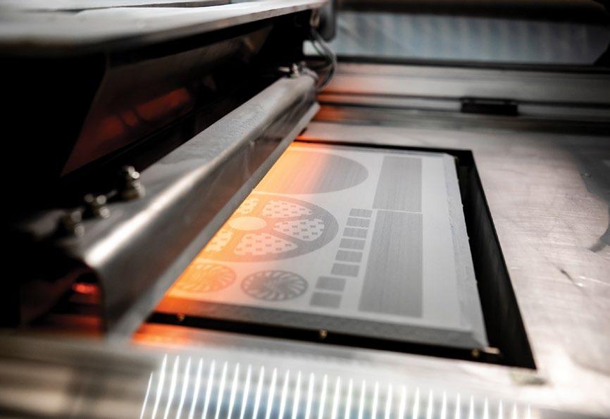
Metal Additive Manufacturing | Spring 2024 52 © 2024 Inovar Communications Ltd Vol. 10 No. 1 | contents | news | events | advertisers | website | newsletter | Industry News www.kennametal.com/am Contact us today to find out how we can help you unlock the full value of 3D printing for your demanding wear, erosion, corrosion, and high-temperature applications. 3D-PRINTED TUNGSTEN CARBIDE WEAR SOLUTIONS METAL POWDERS | PRINTED COMPONENTS | SERIES PRODUCTION
Up to 99.8% less support in Metal PBF
Enclosed parts with low overhangs
Reduced material use
Ease of post-process
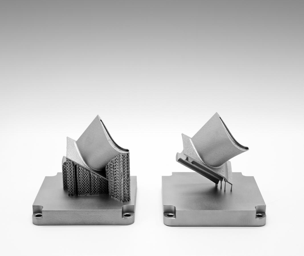
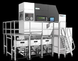
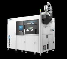



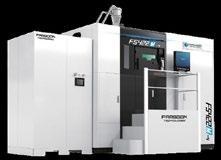
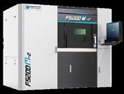
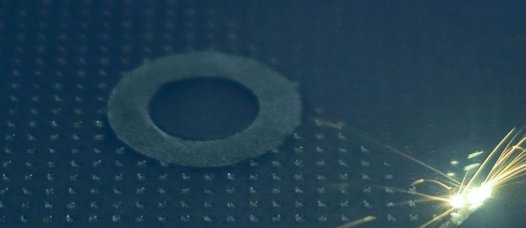

Metal Additive Manufacturing | Spring 2024 53 Vol. 10 No. 1 © 2024 Inovar Communications Ltd
Build Envelope 620×620×1100mm
FS621M-4
Build Envelope 425×425×550mm
FS422M-4
Build Envelope 425×230×300mm
FS200M-2
Build Envelope 433×358×400mm
upport
Meet SRS Technology
With SRS Farsoon Americas Corp | Austin, Texas contact@farsoonam.com Farsoon Europe GmbH | Stuttgart, Germany wehelpyou@farsoon-eu.com Farsoon Technologies | AMEA globalinfo@farsoon.com
FS350M-4
S
R eduction S ystem
Before
farsoon-gl.com
RAM3D adds its twelfth metal AM machine
Rapid Advanced Manufacturing Ltd (RAM3D), based in Tauranga, New Zealand, has added a twelfth metal Additive Manufacturing machine to its fleet: the RenAM 500Q from Renishaw, headquartered in Wotton-Under-Edge, Gloucestershire, UK. The new Laser Beam Powder Bed Fusion (PBF-LB) machine is RAM3D’s first four-laser machine and will offer high-volume production and versatility.
RAM3D has continued to expand its fleet of machines following its relocation to a new facility in 2016. Then, the company had three AM machines from Renishaw and one from Nikon SLM Solutions. Partnering with Renishaw has allowed RAM3D to respond to anticipated customer needs by following a phased rollout
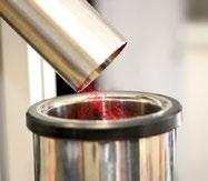
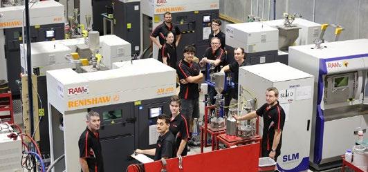
of additional metal AM machines over the past eight years.
“The Renishaw machines offered us the flexibility, openness and easy set up that we were looking for,” the company stated. “We had our own ideas about what we wanted to do in terms of optimising our manufacturing process, and these machines gave us the freedom to implement them.”
The RenAM 500Q, featuring four 500 W lasers, is designed to handle larger production numbers. It has a build volume of 250 x 250 x 350 mm, and features automated powder and waste handling systems that enable consistent process quality, reduces operator intervention and ensures high standards of system safety. www.ram3d.co.nz
www.renishaw.com




Metal Additive Manufacturing | Spring 2024 54 © 2024 Inovar Communications Ltd Vol. 10 No. 1 | contents | news | events | advertisers | website | newsletter | Industry News
Rapid Advanced Manufacturing has added a RenAM 500Q four-laser Additive Manufacturing machine from Renishaw to its fleet (Courtesy RAM3D)
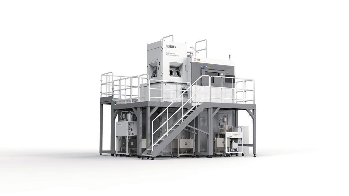
Metal LPBF System
BLT-S615
Build Dimension
600mm×600mm×1500mm (W×D×H)
650mm×650mm×1300mm (W×D×H)
Application Industry
Aviation/Aerospace/Automotive/Engine

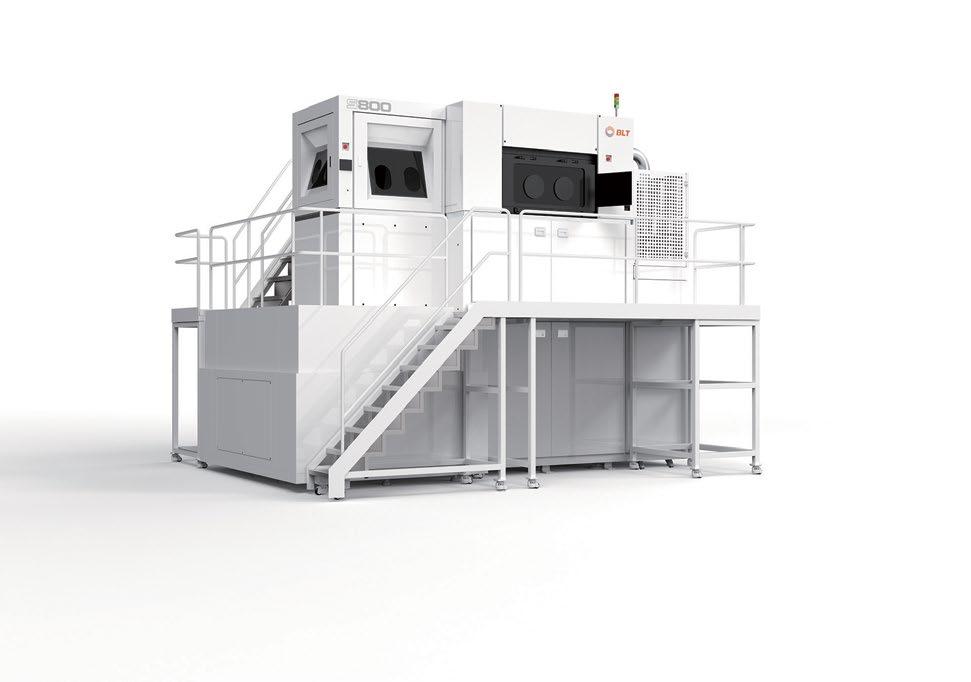
BLT-S800
Build Dimension
800mm×800mm×600mm(W×D×H)
Application Industry
Aviation/Aerospace/Automotive/Engine





BOOTH 2223 Bright Laser Technologies Large Format Metal Printing https://www.xa-blt.com/en/ HessenstraBe 11, 65719 Hofheim am Taunus, Germany +49 6122 1704 058 sales.global@xa-blt.com LinkedIn @Bright Laser Technologies-BLT YouTube @Bright Laser Technologies *BLT reserves the right of final explanation. Health and Well-being in BLT IS09001:2015/IS014001:2015/ IS045001:2018 Laser FDA Safety Certification
Metal LPBF System

THE HOPPER HAS LANDED
Your full-scale AM revolution starts now with the next-gen stainless steel Hopper, a bulk supply of premium AM powder.
• Think big: More than 1 metric ton of powder per Hopper
• Eliminate waste: One Hopper replaces 100+ non-recyclable plastic bottles
• Lock down safety and quality: Minimize contamination, maximize efficiency and traceability
PREMIUM AM POWDER: NICKEL | STEEL | TITANIUM | ALUMINUM | COBALT | COPPER Hop to it: CarpenterAdditive.com/Hopper
Ursa Major’s additively manufactured Hadley engine reaches hypersonic speeds in first flight
Ursa Major Technologies Inc, located in Berthoud, Colorado, USA, has flown its additively manufactured Hadley engine for the first time, reaching supersonic speeds approaching Mach 5. The Hadley engine, designed to meet America’s commercial and national security space needs, was used to power Stratolaunch’s Talon-A1 (TA-1) testbed during a flight over the Pacific Ocean.
The Hadley is a 5,000-pound-thrust (lbf) liquid oxygen and kerosene, oxygen-rich staged combustion cycle rocket engine for small vehicles. Customers can use Hadley to launch small payloads into orbit or hypersonic platforms.
Unlike historical rocket engines, Ursa Major uses metal Additive
Manufacturing to speed up the production process, allowing the company to build engines in a matter of days.
“For the first time since SpaceX fundamentally transformed space launch with privately-developed rockets, Ursa Major and Stratolaunch have come together to advance a critical national mission,” stated Ursa Major founder and CEO Joe Laurienti. “Hypersonic flight has been a massive military and governmental challenge. Today, private companies were able to propel a leap forward.”
Hadley is the first product in a family of propulsion systems, including liquid rocket engines and solid rocket motors, designed, developed, and produced by Ursa
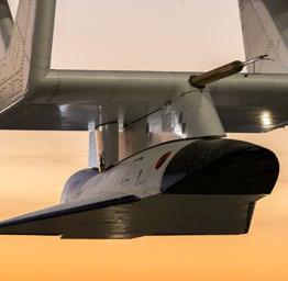
Ursa Major’s Hadley engine was used to successfully power the Stratolaunch Talon-A1 test vehicle during its first powered flight (Courtesy Stratolaunch)
Major. This engine, as well as other Ursa Major products, are said to enable the US Department of Defense to field solutions more quickly and push speed, range and payload metrics.
www.ursamajor.com

Metal Additive Manufacturing | Spring 2024 57 Vol. 10 No. 1 © 2024 Inovar Communications Ltd | contents | news | events | advertisers | website | newsletter | GETPDF Industry News
www.carbolite-gero.com LEARN MORE! EXPLORE HOW THE OXYGEN CONTENT INTERACTS WITH METALS LIKE TITANIUM SOLUTIONS FOR ADDITIVE MANUFACTURING High quality parts in Additive Manufacturing are desirable. During heat treatment processes too many molecules of oxygen may discolor the parts and even change its properties. The correct understanding of the heat treatment process will help to chose the right technology, safe money, and brings your project to a success without unnecessary delay. Carbolite-Gero-Advert-GB-175x120_AM.indd 1 19.02.2024 10:12:37
GPAINNOVA America and Xact Metal partner to streamline metal Additive Manufacturing in dental sector
GPAINNOVA America, based in Sunrise, Florida, USA, a subsidiary of Spain’s GPAINNOVA, has entered a strategic partnership with Xact Metal, State College, Pennsylvania, USA, to offer a complete solution encompassing design, Additive Manufacturing and finishing processes, leveraging the technologies developed by both companies.
The agreement involves the utilisation of GPAINNOVA’s patented dry electropolishing process, known as the DryLyte Technology, as a postprocessing solution for Xact Metal’s metal AM machines. This collaboration aims to streamline the metal AM process, making it more accessible to organisations of all sizes.
Together, the companies will focus on the digitalisation of manual labour in dental laboratories, leading to significant time and cost savings. The process is designed
to be less hazardous, providing a safer and more efficient alternative. By incorporating DryLyte finishing technology with the metal AM process, substantial advantages are expected, including a 60-80% reduction in polishing time compared to non-automated methods, faster manufacturing than traditional casting, and a notable reduction in manual labour. “We are eager to expand our knowledge of how the manufacturing industry integrates the Xact Metal technology into its daily fabrication environment,” stated Jesús Contreras, Business Developer at GPAINNOVA America. “Xact Metal has developed a unique market strategy that creates synergies similar to GPAINNOVA’s; combining our expertise, we can shape the proper perspective for the AM adopters and have a final product to fulfil their needs.”
Armadillo Additive launches advanced Additive Manufacturing facility specialising in titanium medical devices
Armadillo Additive, a contract manufacturer based in Granbury, Texas, USA, has launched its new advanced metal Additive Manufacturing facility targeting precision engineering for the medical device sector. The
company has installed a FormUp 350 Laser Beam Powder Bed Fusion (PBF-LB) Additive Manufacturing machine from AddUp, and will specialise in Ti-6Al-4V Grade 23 titanium products.
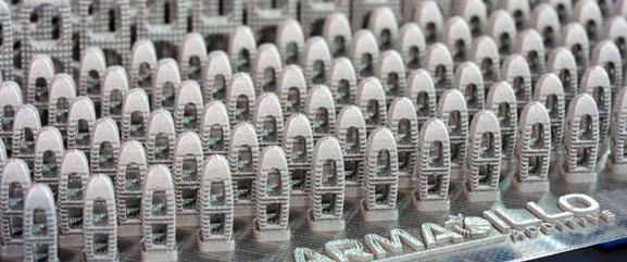
GPAINNOVA’s dry electropolishing
DryLyte process will be incorporated with Xact Metal’s AM technology (Courtesy Xact Metal)
“We are very excited to begin this partnership with GPAINNOVA to offer a full solution from design to finished part using their patented wet and dry electro-polishing,” shared Xact Metal CEO, Juan Mario Gomez. “It allows the customer to automate the finishing process, reducing the need for manual labour and saving them time.”
www.xactmetal.com
www.gpainnova.com
The new facility is complemented by comprehensive in-house services, such as laser marking, heat treatment, and bead blasting, helping it deliver end-to-end solutions that are said to meet the rigorous demands of medical engineering.
Armadillo Additive selected a four-laser FormUp 350 AM machine with a build volume of 350 x 350 x 350 mm. “The FormUp 350 is a dream come true for us,” shared Noah Smith, Armadillo Additive’s Director of Operations. “It’s on the cutting edge from both a software and hardware perspective. The large build volume and quad laser system allow us to get production jobs done faster than the competition, while the roller recoater lets us push the design envelope to the next level.”
www.armadilloadditive.com
www.addupsolutions.com
Metal Additive Manufacturing | Spring 2024 58 © 2024 Inovar Communications Ltd Vol. 10 No. 1 | contents | news | events | advertisers | website | newsletter | Industry News
AM spinal implants made on the FormUp 350 (Courtesy Armadillo Additive)
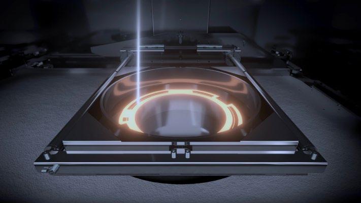
Advancing JEOL’s EB-PBF Printer’s Capability
AMS7032 Operational Qualification: Ti6Al4V Grade 5 samples complied with AMS7011 requirements.
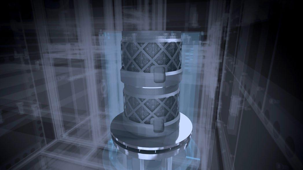
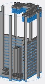
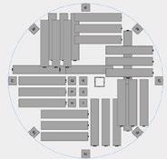
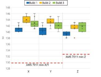
JAM-5200EBM was installed at Cumberland Additive in Pittsburgh in 2023 with another being installed at the Technical University of Munich, TUM School of Engineering and Design.
www.jeol.com
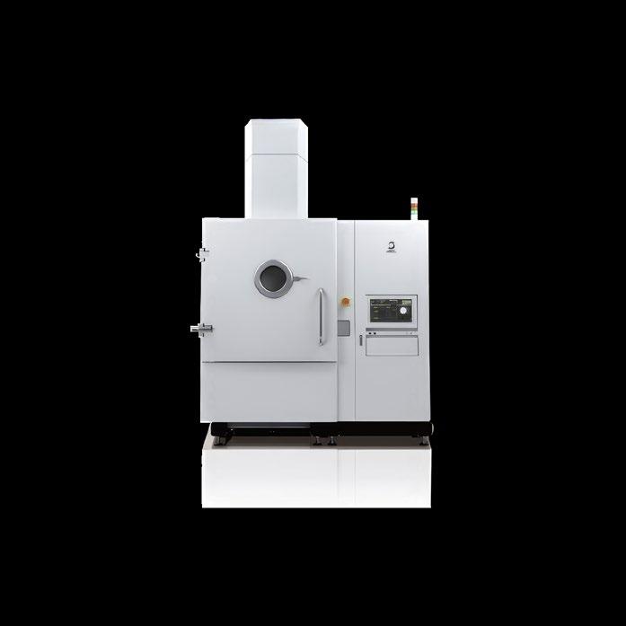

June 25 - 27, 2024
Los Angeles Convention Center
South Hall No.2421
AMS7032 Build Design, ISO and Top Views
Ultimate Tensile Strength
6K again named to Global Cleantech 100 list for UniMelt Platform
6K Inc, based in North Andover, Massachusetts, has been recognised on the Global Cleantech 100 list for the second year in a row. The Global Cleantech 100 is intended to showcase the most promising private companies in the ‘cleantech’ ecosystem. The report aims to offer insight into organisations with outstanding technologies, original business models, and bold plans to act on the ever-increasing climate and environmental crisis.
The recognition is largely driven by the success of 6K’s UniMelt Microwave Plasma Production Platform, which is capable of producing metal Additive Manufacturing powders and battery materials via a fast, clean process.
“When we first introduced the UniMelt platform, one of our goals was to transform manufacturing
of critical materials. Our UniMelt solution takes a sustainability-first approach, replacing outdated, dirty processes with clean and efficient production – dramatically reducing production times from days to seconds at significantly lower carbon emissions than legacy processes,” stated Bruce Bradshaw, Chief Marketing Officer at 6K. “We’re honoured the industry experts at Cleantech Group have once again recognised 6K for our efforts in creating a more sustainable, productive planet.”
This recognition builds on the company’s recent execution of a $50 million award with the US Department of Energy’s (DOE) Office of Manufacturing and Energy Supply Chains for its PlusCAM battery material production plant in Jackson, Tennessee. Additionally,
6K Additive initiated a significant investment programme to expand current capacity and add to its metal processing capabilities. This programme was supported by a $23.4 million grant award for upcycling critical metals for use in key defence applications through the Office of the Assistant Secretary for Industrial Base Policy via its Manufacturing Capability Expansion and Investment Prioritization directorate.
“Companies included in the Global Cleantech 100 like 6K are industry leaders and transformers – driving positive change and at the forefront of powering global transition to a more sustainable future,” shared Richard Youngman, CEO, Cleantech Group. “The Global Cleantech 100 is a recognition of the market’s positive view on their progress to date and their potential impact in building a cleaner, decarbonised world.”
www.6kinc.com
www.cleantech.com
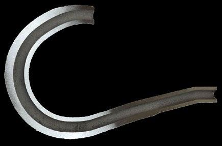
• exceptional wear
•
•
Metal Additive Manufacturing | Spring 2024 60 © 2024 Inovar Communications Ltd Vol. 10 No. 1 | contents | news | events | advertisers | website | newsletter | Industry News VIBENITE® Hardness up to 75 HRC IS WEAR RESISTANCE ON
THE AGENDA?
With our patented Vibenite® alloys you get:
resistance
extreme heat resistance
ening service,
order the
steel with
up to 75 HRC. Get in touch for more information about our unique materials.
VIBENITE® REDEFINING WEAR RESISTANCE Our material Your application A new performance Blasting nozzle cross-section
complex geometry With our in-house Hot Isostatic Pressing and hard-
you can now
world’s hardest
a hardness of
vbncomponents.com
Wayland Additive raises £4.2 million to expand operations and in-house production
Wayland Additive, based in Huddersfield, UK, has successfully secured £4.2 million in funding to expand operations following a successful year of operations.
Wayland designs, develops, makes and sells industrial Electron Beam Powder Fusion (PBF-EB) Additive Manufacturing machines. This latest funding round – led by the UK’s leading investor into university spinouts, Parkwalk Advisors – will enable the company to expand its manufacturing capabilities, further scaling up its operations and expanding its global customer base.
“Wayland has grown exponentially over the past year, with this latest raise representing a major milestone for our business as we continue to seek additional funding over the coming year,” stated Will Richardson, CEO of Wayland. “After a successful 2023, we’re setting our sights on further developing our in-house production capacity and increasing our global customer base to enable more sectors to benefit from our cutting-edge election beam printing technology.”
This funding comes after Wayland Additive rolled out its technology to a range of buyers across different sectors, including aerospace, mining, engineering, medical, motorsport, military, and defence. Customers include Exergy Solutions in Canada and a recent installation in Europe. The company’s operations currently occur across North America and Europe.
Parkwalk Advisors, which has supported Wayland since 2021, invested £2 million as part of this round, which also included longterm backer Longwell Ventures with a total of £4.2 million already raised in the round. This funding round will remain open, with a
target of £10 million. It follows a £4.6 million oversubscribed Series A funding round in April 2023, building on previous funding successes.
Martin Glen, Investment Director of Parkwalk Advisors,
shared, “We are proud to be playing a leading role in growing Wayland Additive as it continues its journey to scale up its operations. Wayland is a prime example of a university spinout driving real positive change by deploying unique, cutting-edge technology to a range of sectors and challenges. We’re excited to see the company grow further.”
www.waylandadditive.com
www.parkwalkadvisors.com

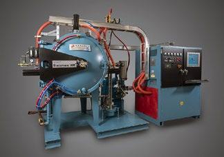
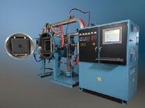
Metal Additive Manufacturing | Spring 2024 61 Vol. 10 No. 1 © 2024 Inovar Communications Ltd | contents | news | events | advertisers | website | newsletter | GETPDF Industry News • Metal or graphite hot zones • Processes all binders for metals or ceramics • Sizes from 8-1500 liters (0.3–54 cu ft.) • Pressures from 10-6 mbar to Atmosphere • Precision heat treating post processing available • Vacuum, Ar, N2 and H2 • Max possible temperature 3,500°C (6,332°F) • Worldwide field service, rebuilds and parts for all makes Centorr Vacuum Industries 55 Northeastern Blvd Nashua, NH 03062 USA Tel: +1 603 595 7233 Fax: +1 603 595 9220 Email: sales@centorr.com www.centorr.com/am Sintervac® AM WorkhorseTM AM Sintervac AM debind and sinter vacuum furnaces for Additive Manufactured parts Over 6,500 production and laboratory furnaces manufactured since 1954 ®
Xact Metal and Uddeholm partner to supply Corrax tool steel for Additive Manufacturing
Xact Metal, State College, Pennsylvania, USA, has announced its partnership with Uddeholm, a voestalpine company headquartered in Hagfors, Värmland, Sweden, to supply Corrax tool steel for Additive Manufacturing. The introduction of Corrax grants Xact Metal customers access to a corrosion-resistant, cobalt-free tool and mould steel capable of superior surface finish post-polishing.
“We are proud of our partnership with Uddeholm,” said Juan Mario Gomez, Xact Metal CEO, “which grants us the ability to offer their revolutionary Corrax metal powder. This intersection between our affordable, high-performing 3D printing technology and Uddeholm’s material expertise is the point where the adoption of Additive Manufacturing can begin serving the tooling and moulding industry. Uddeholm’s rich history and practical knowledge in the steel industry brings a legacy of excellence and innovation to our collaboration.”
Typically, moulders and mouldmakers have faced limitations in
creating optimal internal structures for moulds due to the constraints of traditional manufacturing methods. This solution will bring the unprecedented capabilities of metal Additive Manufacturing to the sector.
“We are excited to be partnering with Xact Metal,” stated Kevin Rochford, Vice-President of Sales from Uddeholm. “This partnership not only signifies a milestone in Additive Manufacturing but also brings in a new era of possibilities for the mould and tooling industry, where complexity meets efficiency, and tradition meets innovation. With our long history in the steel industry, this is a natural step forward for Uddeholm.”
In addition to technological advancements, the environmental benefits of Corrax powder are significant. Uddeholm prioritises sustainable production practices, utilising fossil-free electricity to achieve a fossil-free powder manufacturing process.
www.xactmetal.com
www.uddeholm.com
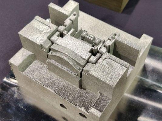
BLT expands presence in South Korea, Baltic Sea region and Africa
Bright Laser Technologies (BLT), located in Xi’an, China, has announced the signing of three distributor agreements that will expand its presence in South Korea, the Baltic Sea Region, and Africa.
South Korea is seen as one of the key locations for BLT’s expansion in Asia, with the company looking to tap into the country’s growing technological landscape. To meet this demand, BLT has partnered with Lincsolution, a leading AM service provider based in Anyang-si, Gyeonggi Province. Together, the companies will focus on delivering turnkey solutions for metal AM in the region, with BLT offering its extensive range of machines and metal powders.
Also announced was a partnership with CadXpert, headquartered in Kraków, Poland, with the aim of bringing BLT to the Baltic regions, including Lithuania, Latvia, and Estonia. As an established distributor of both polymer and metal AM machines from a number of equipment manufacturers, CadXpert will offer post-sales support and services that include equipment installation, maintenance, repair, customer training and CAD design.
In Africa, RusselSmith, a leading energy services provider based in Lagos, Nigeria, will offer BLT’s range of AM machines and powders to West Africa, Namibia, Angola, and Uganda regions. RusselSmith is ISO 9001:2015 and ISO 45001:2018 certified, with a focus on technology solutions for oilfield management, smart manufacturing, and sustainable energy. The company also has a division selling Additive Manufacturing machines and AM components.
en.lincsolution.com
www.cadxpert.pl
www.russelsmithgroup.com
www.xa-blt.com
Metal Additive Manufacturing | Spring 2024 62 © 2024 Inovar Communications Ltd Vol. 10 No. 1 | contents | news | events | advertisers | website | newsletter | Industry News
Xact Metal has announced its partnership with Uddeholm to supply Corrax tool steel for Additive Manufacturing (Courtesy Xact Metal)
Demanding environments require high pressure technology
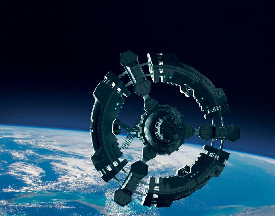
The global leader in high pressure technology
Mission critical parts for rockets, satellites and future space exploration need robust and light-weight solutions to withstand the rigorous demands of launch and long-term space flight. Quintus high pressure equipment is key to improving payload volume by reduction of mass in re-usable launch vehicles and payload structures.
Quintus Technologies designs, manufactures, installs, and supports high pressure systems in three main areas: densification of advanced materials, sheet metal forming and high pressure processing for food and beverage innovation, safety, and shelf life.
Quintus has delivered over 1,900 systems to customers within industries from energy, medical implants, space, aerospace, automotive and food processing. The company is headquartered in Västerås, Sweden, with a presence in 45 countries worldwide.
Visit www.quintustechnologies.com for more information!

www.quintustechnologies.com
Visit us at booth #1300 at Rapid + TCT June 25–27, 2024 Los Angeles Convention Center, Los Angeles, CA
FIT becomes Meltio’s first official service bureau in DACH region
Meltio, headquartered in Linares, Spain, has announced that FIT AG, based in Lupburg, Germany, has become its first official service bureau, and a key contributor to its application development, in the Germany/Austria/Switzerland (DACH) region.
FIT AG provides Additive Manufacturing services to a wide variety of industries and, after verifying Meltio’s wire laser metal deposition (LMD) process, a form of Directed Energy Deposition (DED), has incorporated the technology into its portfolio.
Carl Fruth, founder and CEO of FIT AG, announced, “The laser DED wire technology by Meltio is what appears to be an ideal enhancement of our inventory of AM technologies. We see fantastic opportunities here to develop ground-breaking new
applications all along with our customers.”
The Meltio Engine integrates with both robotic as well as CNC equipment, bringing metal Additive Manufacturing capabilities to a wide range of industries and applications. The process uses commodity welding wire, being a clean, safe and relatively lowest-cost metal feedstock. By adding the Meltio Engine into a robotic arm at its facility, FIT AG hopes to play a key role in making this technology more accessible across the DACH region.
“We are thrilled to be working with FIT AG and KnowHow Wilhelms [Meltio’s first official sales partner for Germany] as this collaboration between us serves as a great indicator of how Meltio’s partner ecosystem is evolving. Together we will be able to cater to the ever-
FIT AG has become the first official service bureau for Meltio in the DACH region, adding the Meltio Engine into a robotic arm at its facility (Courtesy Meltio)
growing interest in Meltio’s technology and its applications. As well as by leveraging FIT’s knowledge, we will be able to further develop the adoption of Meltio unique wire-laser metal Additive Manufacturing for different industries,” shared Moisés Moza Sanchez, Sales Manager in DACH region at Meltio.
www.meltio3d.com
www.fit.technology
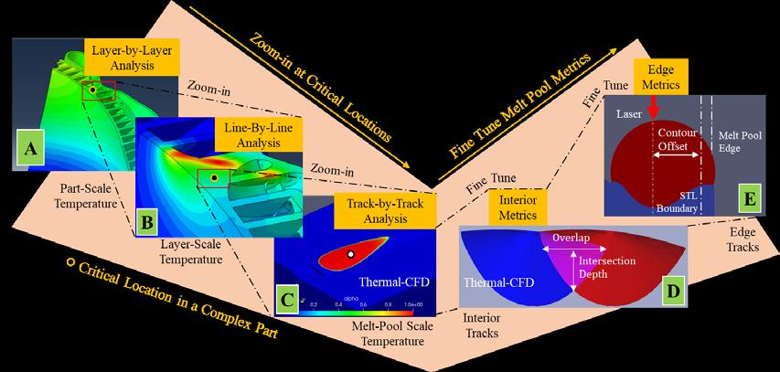


Metal Additive Manufacturing | Spring 2024 64 © 2024 Inovar Communications Ltd Vol. 10 No. 1 | contents | news | events | advertisers | website | newsletter | Industry News
AM Parameter Predictor (AMP2) Applied Optimization, Inc. www.appliedO.com\amp2 Track-by-Track High-Res Melt Pool Thermal Imaging Validated AM Parameter Prediction Technology Predict Optimize Defects US Patent No: 11,915,405 B2

SPECIALTY MATERIALS SHAPING
THE FUTURE OF MANUFACTURING
PERFORMANC
P r i m a r y p o w d e r p r o d u c e r G l o b a l m a n u f a c t u r i n g n e t w o r k A l u m i n u m , C o p p e r , T i t a n i um & c u s t o m a l l o y s F l e x i b i l i t y f o r c u s t o m d e v e l o p m e n t w i t h a b i l i t y t o s c a l e C o n t r o l o f p o w d e r a t t r i b u t e s f o r g r e a t e r p e r f o r m a n c e S p e c i a l i z e d p r o c e s s e s t a i l o r e d t o y o u r n e e d s T r u s t e d g l o b a l l e a d e r i n m e t a l p o w d e r s a n d a l l o y s
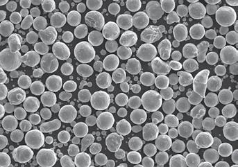
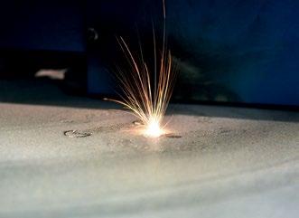
INNOVATION
D e e p t e c h n i c a l e x p e r t i s e a n d v a s t R & D c a p a b i l i t i e s
P o w d e r s f o r B i n d e r J e t t i n g , P o w d e r B e d F u s i o n & D E D
C u s t o m i z e d s e r v i c e s , i n c l u d i n g C o l d S p r a y & C o a t i n g s
P r o p r i e t a r y a t o m i z i n g t e c h n o l o g i e s
E x t e n s i v e s i n t e r i n g k n o w l e d g e I n v e s t m e n t i n e q u i p m e n t a n d p a r t s p r o d u c t i o n
PARTNERSHI
P r e m i e r d e v e l o p m e n t a n d p r o d u c t i o n p a r t n e r D e c a d e s o f e x p e r i e n c e p r o d u c i n g h i g h q u a l i t y m a t e r i a l s S p e c i a l i z e d p o w d e r m o r p h o l o g y , c h e m i s t r y & p a r t i c l e s i z e s S u p p o r t o f c r i t i c a l a p p l i c a t io n s a t a n i n d u s t r i a l s c a l e
P r i m e d t o f o r t i f y t h e r a p i d l y g r o w i n g A M m a r k e t
www.kymerainternational.com | info@kymerainternational.com
Kittyhawk acquires Stack HIP from Stack Metallurgical Group
Kittyhawk, Inc, Garden Grove, California, has announced that it has acquired Stack HIP, LLC, Albany, Oregon, from Stack Metallurgical Group (SMG). With the backing of Dallas-based private equity firm Trive Capital, the acquisition represents a significant expansion of its Hot Isostatic Pressing (HIP) capacity and capabilities for aerospace, space, defence and medical applications.
“SMG built a world-class facility in Stack HIP. With this acquisition, Kittyhawk is the premier provider of HIP services on the West Coast. We look forward to supporting our customers’ growth and will continue to make significant investments in capacity to meet the demands of our growing customer base,” commented Tanner Cope, Managing Director at Trive.
Stack HIP provides HIP services to aerospace, defence, and medical customers. The company reportedly possesses the largest high-pressure HIP vessels in North America, enabling the processing of the biggest and most complex castings and additively manufactured
metal parts. Post-closing, SMG will continue to operate its classical heat treatment and aluminium special processing facilities in Portland, Oregon; Spokane, Washington; and Salt Lake City, Utah.
“We’re excited to welcome Stack HIP customers, employees, and suppliers into the Kittyhawk family,” said Brandon Creason, President of Kittyhawk. “Stack HIP will allow Kittyhawk to service mission critical parts up to 160 cm in diameter, enabling us to process the full array of components for our customers.
At Kittyhawk, we commit every day to providing the best service and quality to our customers, and we’re thrilled to now do that with the added capabilities and dedicated employees of Stack HIP. We look forward to the continued relationship with SMG to deliver unmatched special processing services to our valued customers.”
Doug Puerta, CEO of SMG commented, “We look forward to continued collaboration with Kittyhawk to deliver a differentiated level of service, quality, and value to our shared customers. This transaction will allow both companies

Stack Metallurgical Group entered the Hot Isostatic Press market in 2019 with the addition of a QIH 286 Mega-HIP manufactured by Quintus Technologies (Courtesy Stack Metallurgical Group)
to further drive capacity, quality, and capabilities in our respective services to best serve the PNW market.”
“This is an important step in growing the platform specialised in this highly-differentiated HIP capability. The Company continues to benefit from strong industry tailwinds, and we are excited to support our customers by investing in capacity,” said David Stinnett partner at Trive.
www.trivecapital.com
www.stackmet.com
www.kittyhawkinc.com








Metal Additive Manufacturing | Spring 2024 66 © 2024 Inovar Communications Ltd Vol. 10 No. 1 | contents | news | events | advertisers | website | newsletter | integrated sintering furnace for high volume production additive manufacturing technical ceramics powder metallurgy hard metals high vacuum, inert gas, hydrogen benchmark for cleanest atmosphere combinded debinding & sintering furnace from laboratory scale to high volume production MUT ADVANCED HEATING 30 YEARS MUT FURNACES: MUT ADVANCED HEATING MUT FURNACES: Industry News

● GAS AND ULTRASONIC ATOMIZERS FOR SPHERICAL POWDERS WITHOUT ANY SATELLITES for LPBF, MIM, Binder Jetting and other Additive Manufacturing applications. High purity, sphericity and wide range of reproducible particle size distribution.
● WATER ATOMIZERS FOR MORE IRREGULAR POWDERS ideal for recycling/refining process, press & sinter process and others.
● AIR CLASSIFIERS FOR THE PRECISE SEPARATION OF METAL POWDERS into fine and coarse powder fractions especially in the range < 25 µm
● MAXIMUM PURITY BY OXIDATION-FREE PROCESSING
● FOR A WIDE RANGE OF METALS AND FOR SMALL TO MEDIUM AMOUNTS
● ALL SYSTEMS DESIGNED FOR EASY HANDLING AND CLEANING, QUICK ALLOY CHANGE WITH MINIMUM CROSS CONTAMINATION
www.bluepower-casting.com
BLUE POWER. EQUIPMENT & EXPERTISE FOR YOUR METAL
POWDER PRODUCTION
Ultrasonic atomization
75045 Walzbachtal · Germany · Phone +49 7203 9218-0 · E-mail: info@bluepower-casting.com
Gas atomization
Atomizer powered by AMAZEMET Air Classifier AC series Inert gas air classification on AC 1000 G
Ultrasonic
AddUp appoints Julien Marcilly CEO
Julien Marcilly has been appointed Chief Executive Officer of AddUp, Cébazat, France, succeeding Frank Moreau. Prior to this appointment, Marcilly served as the Deputy Chief Executive Officer at the company since 2019.
Before joining AddUp, Marcilly worked in leadership roles with the Fives Group for almost fifteen years. As the CEO of Fives Conveying, Marcilly was committed to helping the world’s largest automakers enhance machine productivity with smart automation solutions. Prior to Fives Conveying, Marcilly was successful as the Operations Director of Fives Stein supporting large projects and optimising production lines for steel and glass manufacturers across Europe, Asia, and North and South America.
With a background in traditional manufacturing methods, Marcilly believes that metal Additive Manufacturing has the potential to revolutionise the manufacturing industry. It was stated that he is committed to demonstrating AddUp’s ability to fully support large industrial companies on their Additive Manufacturing journey.
“AddUp is a bonafide Additive Manufacturing OEM built upon the pedigree of our parent companies, industry pioneers Michelin and Fives,” shared Marcilly. “We understand the world of manufacturing because we were born from it. We understand industrial challenges because we have lived them. This is why we are industrialising Additive Manufacturing. We know how to use it, qualify it, and scale it, making it a reliable and repeatable solution for our customers.”
Marcilly said that anticipating the future of Additive
Manufacturing will be a top focus, with priorities on productivity and repeatability, sustainability, software monitoring and data management, all while providing exceptional customer support so that they may realise the full potential metal Additive Manufacturing has to offer.
“AddUp not only has best-in-class PBF and DED machines, but also a best-in-class service team to fully support our customers throughout their Additive Manufacturing journey from design to production and qualification,” explained Marcilly. “I am excited to see the future of Additive Manufacturing and proud to be at the forefront with AddUp, industrialising the technology to solve manufacturers’ toughest challenges. I look forward to leading such an innovative company and to driving the growth of our industry.”
www.addupsolutions.com


Metal Additive Manufacturing | Spring 2024 68 © 2024 Inovar Communications Ltd Vol. 10 No. 1 | contents | news | events | advertisers | website | newsletter | Industry News
Accuron Technologies boosts investment in WAAM3D
Accuron Technologies, based in Singapore, has announced an additional investment and the acquisition of a majority stake in its associate company, WAAM3D Ltd, located in Milton Keynes, UK.
“We are excited about our journey with WAAM3D,” said Tan Kai Hoe, Group CEO and president of Accuron Technologies. “As the company’s first strategic investor when it was spun out of Cranfield University, we provided additional resources to support its growth as the company developed. I see this as a testament to the shared belief the founders and we have in the company, as well as the mutual trust we have developed over the past years.”
Hoe added, “In addition to providing financial support, Accuron’s industrial expertise and network also help to accelerate the company’s technology, product, and business development, but we think it takes a village to raise a child. Indeed, we look forward to working with partners and customers in a long-term relationship to bring this innovative, energy-efficient, and disruptive WAAM technology to key manufacturing industries. I am convinced WAAM will enable us to serve these industries to shape better lives.”
WAAM3D, founded by Cranfield University in 2018, is a spin-out company created to commercialise WAAM technology developed by its leading research group. The aim of the company is to provide industry with the ability to manufacture parts using the technology. In late 2019, Accuron provided initial investment funding for WAAM3D’s transition into an independent entity. Since then, WAAM3D has successfully developed complete turnkey solutions through in-house development and strategic partnerships, to address its customers’ needs for WAAM equipment, dedicated software, wires, parts, and part-making expertise. WAAM3D continues to work closely with Cranfield University, ensuring that the company’s products and services are always at the forefront of new technological innovation in wire-based Directed Energy Deposition (DED) Additive Manufacturing.
WAAM3D uses advanced WAAM techniques allowing manufacturers in the aerospace, oil and gas, mining, semiconductor, and other industries to create largeformat parts. They have greater design freedom, lower costs, a reduced environmental footprint, and shorter lead times.
WAAM3D and Accuron have also established Addept3D, a WAAM application centre based in Singapore. This joint venture seeks to develop and advance the technical expertise necessary to implement WAAM for parts manufacturing in Singapore and the surrounding region.
www.accuron.com
www.waam3d.com
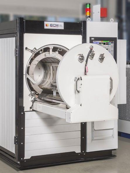
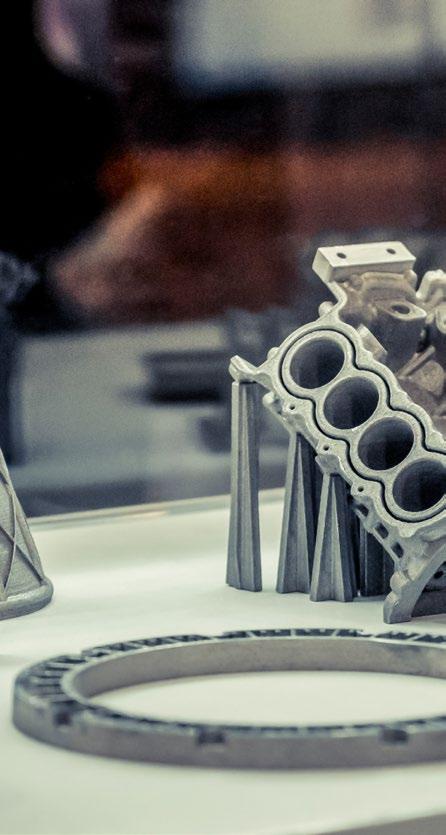

Metal Additive Manufacturing | Spring 2024 69 Vol. 10 No. 1 © 2024 Inovar Communications Ltd | contents | news | events | advertisers | website | newsletter | GETPDF Industry News VACUUM TREATMENTS OF 3D PRINTED METAL PARTS A GLOBAL OFFER ONE SUPPLIER AUTOMOTIVE - AERONAUTICS - MEDICAL
KBM Advanced Materials to distribute Sandvik Osprey metal Additive Manufacturing powders in the USA
Metal powder producer Sandvik AB, headquartered in Stockholm, Sweden, has announced that KBM Advanced Materials, LLC, based in Fairfield, Ohio, USA, will distribute its range of metal powders for Additive Manufacturing across the USA.
KBM, established in 2021, provides a unique supply network in the United States that helps bridge the gap between a dispersed customer base and metal powder producers. The collaboration will increase the availability of Sandvik’s Osprey metal powders in the region.
“We are thrilled to offer our customers in the United States easy access to our market-leading range of Osprey metal powders,” stated Andrew Coleman, Head of metal powder and Additive Manufacturing at Sandvik. “We are seeing increasing demand for our high-quality powders and have listened to our customers’ needs for a US-based stock with short delivery times. We are very proud to offer a customer-centric business solution that will enable them to access high-quality alloys fast, without compromising on quality.”

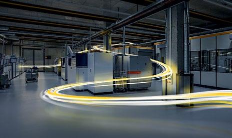
CROSS-DIMENSIONAL
We set the pace to keep you a step ahead of the competition.
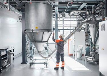
Sandvik is a leading producer of metal powders for advanced manufacturing processes such as Additive Manufacturing and Metal Injection Moulding (Courtesy Sandvik AB)
In April 2023, Sandvik announced the launch of its e-commerce platform, Osprey Online, designed to offer the European market a range of metal AM powders directly from stock. The partnership with KBM is expected to bring the same quick access to its Osprey metal powders in the US.
Luke Harris, Sales Director for metal powder business at Sandvik, added, “We often say ‘The Right Partner is Everything’, and that is certainly as true for us as it is for our end users. KBM shares Sandvik’s focus on creating value for our customers and we feel very optimistic having entered this partnership to provide the US market premium metal powders quickly and efficiently. Our wide range of Osprey metal powders is well-known and trusted across several demanding industries, thanks to our long-standing experience, unique level of traceability, and overall quality. I’m convinced our metal powder offering in combination with KBM’s attractive platform will prove beneficial to our US customers.”
KBM offers a wide range of ready-to-order metal powders to customers in the metal AM and Metal Injection Moulding (MIM) sectors through its online shop system.
“KBM is excited to partner with Sandvik to increase accessibility of Osprey metal powders in the United States,” stated Kevin Kemper, KBM CEO. “On-demand availability of products drives growth in the metal powder industry, and our e-commerce solution features an easy-to-use interface, secure online transactions, detailed product information, pricing transparency, and the ability to ship products within a day of purchase. Our customers will embrace the addition of Sandvik’s quality products to the KBM marketplace, increasing demand for Osprey metal powders.”
www.kbmadvanced.com
www.metalpowder.sandvik
Metal Additive Manufacturing | Spring 2024 70 © 2024 Inovar Communications Ltd Vol. 10 No. 1 | contents | news | events | advertisers | website | newsletter | Industry News
Maker for High-End Precision Parts www.toolcraft.de/en
additive manufacturing, robotics, machining to injection moulding, mould making and quality assurance – with toolcraft by your side, you can unleash the power of innovation. As your technology partner, we bring together additive and subtractive manufacturing across the production process. This creates a unique consulting and manufacturing standard.
Pace
From
MANUFACTURING
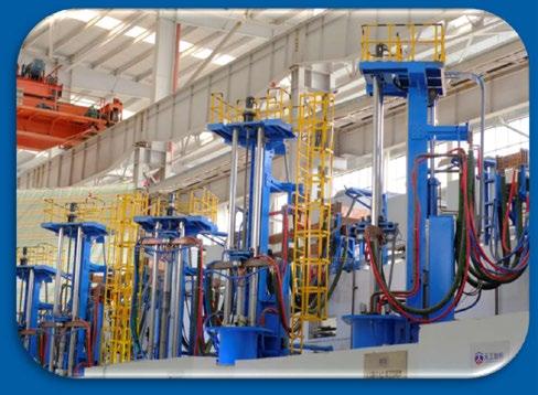
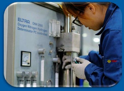
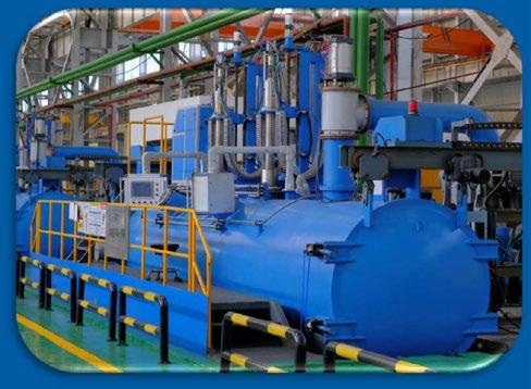
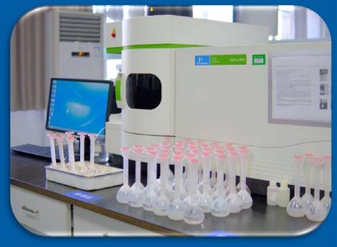

Aerospace-Grade Titanium Wire and Bars for Atomization High-End Manufacturing Equipment Rigorous Quality Control Engineering Support Facilitated Qualification Process Visit our new website: Tiangongti.com
Michelin adds sixth FormUp 350 for the production of tyre moulds
Michelin Moulding Solutions (MMS), based in Greenville, South Carolina, USA, has purchased its second FormUp 350 Laser Beam Powder Bed Fusion (PBF-LB) Additive Manufacturing machine from AddUp SAS, headquartered in Cébazat, France. The new machine represents the sixth to be added to Michelin’s expanding global fleet of FormUp AM machines, currently in use across Europe and North America.
MMS is Michelin’s worldwide division for production of tyre curing moulds. From locations in Europe, Asia and North America, MMS supplies moulds to Michelin’s tyre
manufacturing plants throughout the world. The complex tyre geometries demanded by Michelin to deliver superior tyre performance require equally complex mould geometries which can’t always be produced with traditional manufacturing processes. For almost twenty years, MMS has used metal Additive Manufacturing to meet those demands.
“MMS is very pleased with the productivity and quality achievable on AddUp’s FormUp 350. This level of productivity allowed us to decommission older and less productive 3D printers. We’ve seen improvements in the cleanliness and
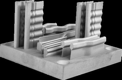
safety of our operations and our operators very much appreciate its ease of use from build plate programming to machine set up and the machine user interface,” explained Glen Nelson, Technical Development Manager at MMS.
One FormUp 350 can reportedly manufacture the quantity of tyre mould inserts which previously required five metal Additive Manufacturing machines and can achieve it faster and more reliably. By using metal AM, MMS has reportedly been able to produce millions of mould sipe inserts over the past two decades, with increasingly sophisticated shapes, to improve traction and wear over the life of the tyre.
www.addupsolutions.com
www.michelin.com
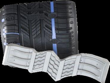
KSB Group first to receive DNV AMC 3 certification for Additive Manufacturing
The KSB Group, headquartered in Frankenthal, Germany, is reported to be the first manufacturer to be awarded the DNV facility qualification certificate AMC 3 for the Additive Manufacturing of ALLOY 625.
KSB is a manufacturer of pumps and valves and has, over the past ten years, built comprehensive expertise in Additive Manufacturing using metal-based Powder Bed Fusion (PBF) at its site in Pegnitz, Germany, where it operates four systems for this type of Additive Manufacturing. In the Additive Manufacturing Center,
specialists work with materials such as stainless steel, nickel-based alloys and other iron-based metal powders.
One of the systems was awarded the ‘Qualification of Manufacturer’ certificate to DNV-SE-0568 and DNV-ST-B203 at Level AMC 3 for the impeller part family. All other Additive Manufacturing facilities have been approved as Level AMC 1 for all part families. With this certification, supplying spare parts quickly –especially to plant operators in the oil and gas industry and the power station sector – will be an option in the future.
Using Additive Manufacturing for producing new and spare parts creates opportunities for operators to order spare parts ‘on demand’ and reduce their spare parts stock, particularly for upstream, midstream and downstream applications of the oil and gas industry.
With a system certified to DNV’s highest level, AMC 3, KSB will be able to supply a large number of spare parts made by Additive Manufacturing, meeting the most stringent of standards in the oil and gas industry or drastically shortening the delivery times of new pumps or valves.
www.ksb.com/en-global
Metal Additive Manufacturing | Spring 2024 72 © 2024 Inovar Communications Ltd Vol. 10 No. 1 | contents | news | events | advertisers | website | newsletter | Industry News
The build plate with tyre sipe mould inserts (left), and the tyre showing the tread pattern produced (Courtesy AddUp)





A erospace P ower Generation B iomedical E lectronics O il & Gas M ilitary Serving the HIP industry for over 45 years Pressure Technology, Inc Warminster, PA | 215-674-8844 Concord, OH | 440-352-0760 Alachua, FL | 386-518-0502 www.pressuretechnology.com IS O 9001/AS9100 13 HIP Units in Continuous Operation Units to 30" in Diameter and 105" in Length with Pressures to 30,000 psi and Temperatures to 2550°F Improving Properties of AM Parts 415 Patricia Drive Warminster, PA 18974 7996 Auburn Road Concord, OH 44077 13451 NW 104th Terrace Alachua, FL 32615 Serving the Northeastern, Mid-Atlantic, Midwestern and Southeastern United States BOOTH 2367
NCMT signs exclusive UK & Ireland distribution agreement with Tritone
NCMT Limited, headquartered in Coventry, UK, has signed an exclusive distribution agreement with metal and ceramic Additive Manufacturing machine maker Tritone Technologies, based in Rosh-Ha’ayin, Israel. Through this partnership, Tritone is seeking to expand its global presence in the UK and Ireland. This agreement will also enable NCMT to transition from conventional machining to Additive Manufacturing solutions.
“We are excited to start our partnership with Tritone Technologies, seeing them as the owners of a groundbreaking technology poised to influence the AM market in the coming years,” stated Jonathan Smart, Managing Director, NCMT. “As a company renowned for its commitment to innovation and cutting-edge technology, this strategic move positions NCMT at the forefront of industrial advancement. We are now
entering the AM sector, elevating our capabilities to meet the evolving demands of modern industry. The integration of Tritone’s advanced MoldJet technology not only diversifies our company’s portfolio but also solidifies its position as a leader in shaping the future of precision engineering and manufacturing.”
Tritone has two AM machines in the market: the Dominant and the Dim. These machines use Tritone’s MoldJet technology, a ‘powder-free’ Additive Manufacturing technology that enables industrial production of high-quality metal and ceramic parts at an industrial speed. Designed for producing a large quantity of high-density parts with complex geometries, MoldJet enables a simplified changeover between a wide variety of metals and ceramics for parallel Additive Manufacturing of parts of various sizes, shapes, and applications.
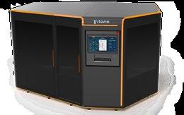
NCMT customers will now be able to buy Tritone Dominant (above) and Dim (Courtesy Tritone Technologies)
“We are delighted to join forces with NCMT in a strategic partnership, emphasising Tritone’s commitment to advancing AM on a global scale,” added Omer Sagi, VP Products and Business Development at Tritone.
“The decision by NCMT to embrace Tritone’s MoldJet technology as their gateway into the AM market is a testament to the innovation and transformative capabilities of our technology. Together, we eagerly anticipate pushing the boundaries of manufacturing excellence and shaping the future of industrial production.”
www.tritoneAM.com
www.ncmt.co.uk
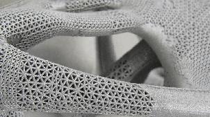
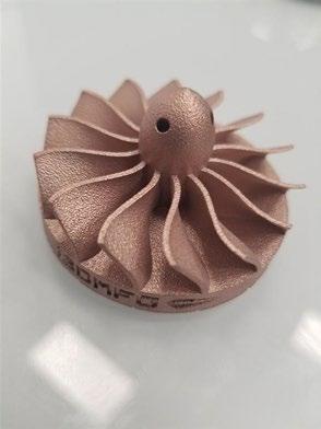
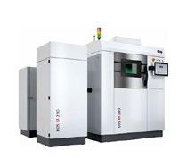
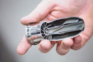
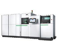
Metal Additive Manufacturing | Spring 2024 74 © 2024 Inovar Communications Ltd Vol. 10 No. 1 | contents | news | events | advertisers | website | newsletter | Industry News
Authentise announces generative AI and 3D annotation for Threads software
Authentise, based in Philadelphia, Pennsylvania, USA, has announced new features for Threads, its collaboration software, that allows users to share, discuss and manage engineering projects. These innovations are said to build on many months of close collaboration with existing Threads users, including the US Department of Defense and Boeing.
New features include the ability to:
• Natively annotate 3D models and tie those comments back to broader conversations related to the project
• Use AI-generated suggestions to capture milestones related to the user’s conversations
• Tie teams together into a synchronous conversation about

Sizes
Work
Operating
a 3D model, allowing users to see each colleague’s point of view
Summarise each Thread with AI to make it easier for colleagues to understand the context of each conversation
Investigate the content of individual customer threads using the AI-powered Threads Andre Wegner, CEO of Authentise, commented, “The continuing disruption to supply chains and pressure to innovate highlights the need for tools that can help us turn ideas into parts, faster. By listening to our customers, it’s become clear that enabling 3D annotation, deepening collaboration opportunities as well as enriching insights and tracking with AI can do just that.”

Following close collaboration with Threads users, Authentise has announced a host of new features for Threads (Courtesy Authentise)
The R&D organisation of a leading surgical robotics company was reportedly working on the platform in less than thirty minutes. Within two weeks, it was reportedly seeing a 1.5X ROI, tracking 100% of its R&D decisions digitally while saving 150 hours and twenty meetings across a distributed team, including external partners. It doubled the effective size of its team.
www.authentise.com
to


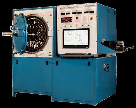
Metal Additive Manufacturing | Spring 2024 76 © 2024 Inovar Communications Ltd Vol. 10 No. 1 | contents | news | events | advertisers | website | newsletter | Industry News VACUUM FURNACES FOR POST ADDITIVE MANUFACTURING www.tmvacuum.com +1-856-829-2000 info@tmvacuum.com Perfect choice for stress relieving, solution treatment, ageing, sintering, brazing or other thermal processes
metal hot zones High vacuum, bright and shiny Integrated quick cool Controlled atmosphere ±3°C uniformity
All
from
0.25 to 16ft3 (7-453l)
(23-726kgs)
loads from 50
1,600lbs
pressure 10-6 torr
T-M Vacuum Products, Inc. Cinnaminson, NJ Super Series High Vacuum Furnace BOOTH 1001
to 6 bar
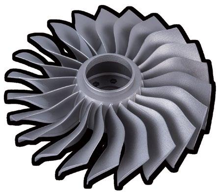

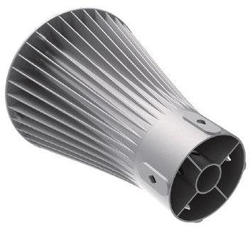


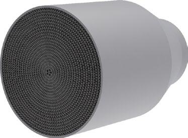

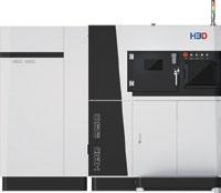
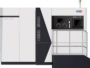
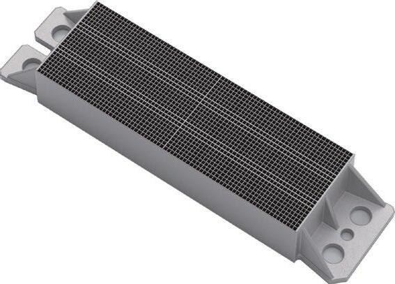
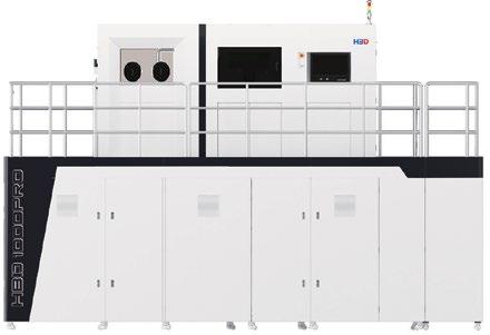




KOREA, 1-5 APR ITALY, 16-18 MAY SPAIN, 3-7 JUN TURKEY, 5-8 JUN USA, 25-27 JUN
REAL-WORLD APPLICATIONS OF HBD METAL AM SYSTEMS
Norsk Titanium expands part production capabilities at USA facility
Norsk Titanium, headquartered in Hønefoss, Norway, is expanding part production capabilities at its Plattsburgh, New York, USA, facility with the addition of heat treatment, ultrasonic non-destructive testing (NDT), finish machining operations, and coordinate measuring (CMM).
The new equipment will enable Norsk to perform the necessary tasks for designing, developing, and qualifying parts, without the extra time required when outsourcing these operations.
“With our RPD Builder rapid part design tool and these new capabilities, we can now take a customer’s final part geometry, design the RPD preform, and validate the design all at our Plattsburgh, New York, facility,” stated Steve Eaton, Norsk Titanium VP of Operations. “We will be able to verify parts in accordance our customers’ aerospace material specifications in as little as six weeks.”
The expanded capabilities will also allow the delivery of limited production rapid prototypes to customers,
Vectoflow raises €4 million for energy and aerospace instrumentation expansion
Vectoflow, based in Gilching, Germany, announced the successful completion of its Series A investment round with €4 million in funding. The funds raised will be used to drive Vectoflow’s expansion into serial production for instrumentation tailored to the aerospace and energy market. The company aims to extend its reach globally by collaborating with new partners.
“We’re preparing for future expansion by strengthening our in-house capabilities,” stated Christian Haigermoser, co-founder and co-CEO of Vectoflow. “This includes ramping up Additive Manufacturing, improving part post-processing, optimising instrumentation assembly, enhancing sensor calibration, and developing software solutions for test rig data acquisition and control. Our extensive know-how in flow instrumentation design, manufacturing, and calibration will play a crucial role in supporting business development across various markets.”
Founded in 2014, Vectoflow produces standardised and customised flow measurement technology for various applications.
Flow measurement systems and Air Data Systems from Vectoflow accurately measure the static pressure, total pressure, velocity, and angle of attack of a flow. These systems are adapted to their respective field of application in wind energy, aviation, turbomachinery development, and research, in terms of shape, size, and material. The manufacturing process is said to greatly increase their robustness, enabling reliable functioning under challenging environmental conditions.
The closure of the investment round is said to demonstrate confidence in Vectoflow’s capabilities; investors include new key players such as Bayern Kapital Innovationsfonds II, WN Invest GmbH, One Investment GmbH, argo vantage GmbH, Schwarz Holding GmbH, and Dr Rolf Pfeiffer. Additionally, existing seed investors AM Ventures and KfW Bankengruppe also participated.
“We are proud of having supported Vectoflow from its early stage,” stated Johann Oberhofer, Managing Partner of AM Ventures. “Katharina Kreitz and Christian Haigermoser recognised that industrial 3D printing
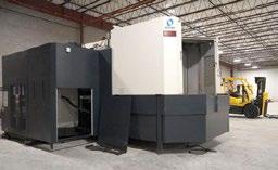
Norsk Titanium is adding heat treatment, ultrasonic non-destructive testing, finish machining operations and coordinate measuring at its facility in Plattsburgh USA (Courtesy Norsk Titanium)
and is in line with the company’s objective of developing a ‘part-in-aday’ operation.
www.norsktitanium.com
is predestined for fluid-dynamic metrology devices due to its freedom of design allowing very complex structures. The fact that Vectoflow’s customers are now directing their attention towards series production projects underscores the expertise they have diligently cultivated over the years in the R&D sector. With both existing and new partners on board, we are looking forward to support their further development and growth into series manufacturing.”
Monika Steger, Managing Director of Bayern Kapital, commented, “We are delighted to support Vectoflow in its continued growth. This dynamic and innovative company, with its futureoriented high-tech solutions and a high degree of innovation, embodies the kind of innovation and technological advancement we want to promote. Their impressive development and forward-looking solutions align excellently with our commitment to nurturing visionary companies.”
Katharina Kreitz, co-founder and co-CEO, concluded, “Our track record has built trust among our current customers, which we plan to leverage for expansion in existing and new markets. I’m particularly enthusiastic about our ventures into aerospace and wind energy applications, as these are future markets with significant societal relevance.”
www.vectoflow.de
Metal Additive Manufacturing | Spring 2024 78 © 2024 Inovar Communications Ltd Vol. 10 No. 1 | contents | news | events | advertisers | website | newsletter | Industry News

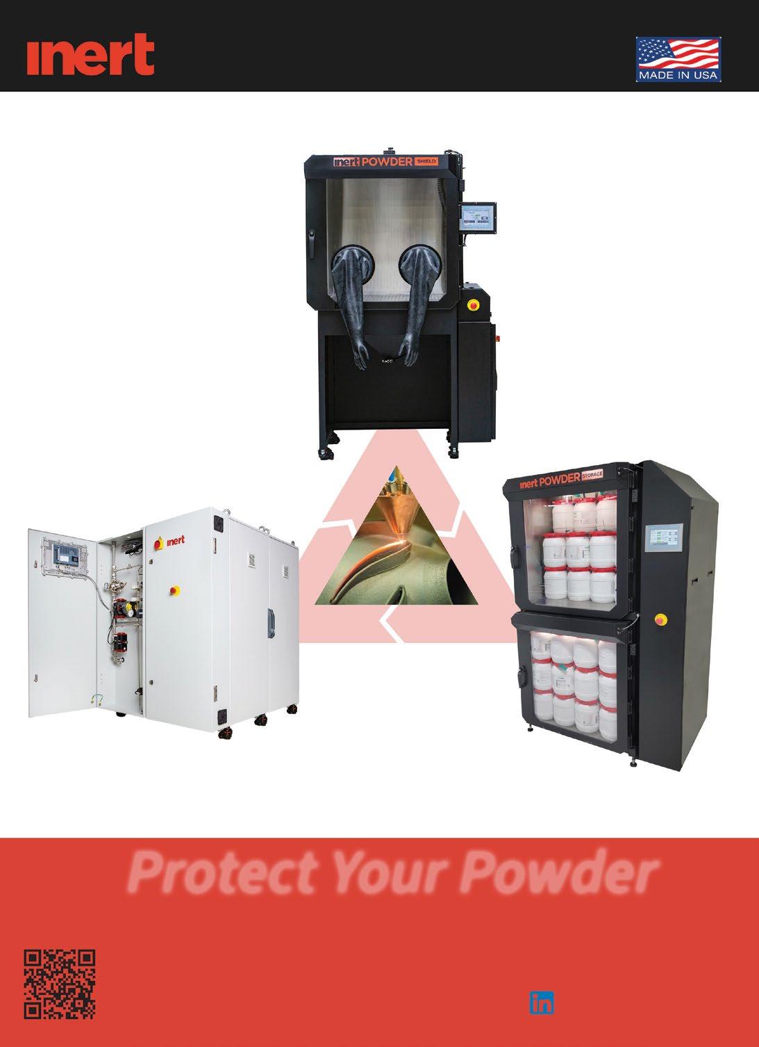


Volkmann and EOS GmbH offer automated metal powder management systems for Additive Manufacturing
Volkmann, Soest, Germany, and EOS GmbH, located in Krailling, Germany, have entered into a cooperation agreement to offer a new line of Volkmann’s automated metal powder management systems. The systems are designed to seamlessly integrate
with the EOS M 400 series metal Additive Manufacturing machines.
The new EOS Edition line of metal powder management systems will facilitate the transfer and loading of material from storage into one or more AM machines, capture and sieve
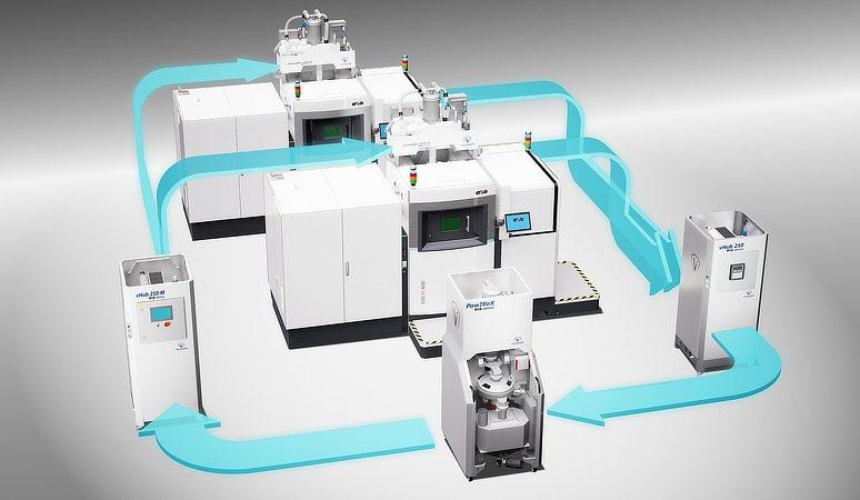
TriAlCo and Fehrmann partner to produce AlMgty aluminium alloy in North America
TriAlCo, a leading North American aluminium manufacturer based in Chicago Heights, Illinois, USA, and aluminium alloy developer Fehrmann, headquartered in Hamburg, Germany, have entered into a partnership following the signing of a Know-how and License Agreement.
Under the agreement, TriAlCo is now licensed to market and produce Fehrmann’s AlMgty aluminium alloy. AlMgty is noted for its strength and elongation performance. It is corrosion-resistant, can be anodised in various colours and can reduce weight by 20-30%
without sacrificing strength, making it well-suited to industries looking for lighter and more efficient materials.
“AlMgty is not just a product,” stated Jay Armstrong. “It’s a catalyst for change in the aluminium industry. Its unique blend of strength and ductility, sustainability, and efficiency sets a new standard for what our clients can expect.”
Henning Fehrmann added, “Our collaboration with TriAlCo is a testament to our commitment to innovation and sustainability. AlMgty is the result of years of research and
excess powder for reprocessing, and the automated vacuum drying of metal powders. Additionally, buffer storage units and other accessories are also available with the new systems.
The EOS Edition is now available in North America through EOS North America. This edition can function as a sealed circuit, which can help eliminate metallic dust from the workplace, enabling worker safety and protecting the metal powders from ambient moisture and contamination. The system is scalable, can be operated unattended 24/7 and can be controlled and monitored remotely.
“Our new systems provide EOS end-users with a complete, plug-and-play, automated powder handling solution that can scale as their production needs increase,” stated Christian Mittman, director of advanced solutions for Volkmann. “This is a logical next step in our close relationship with EOS, and one that we feel will benefit EOS customers with faster, safer, more reliable printing and consistently high-quality printed parts.”
uk.volkmann.info
www.eos.info

Henning Fehrmann, CEO and chairman of Fehrmann
and Jay Armstrong, president of TriAlCo, have signed a Know-how and License Agreement between the two companies (Courtesy Fehrmann)
development, and we’re excited to see its impact across North America. It is a milestone for our internationalisation.”
www.trialco.net
www.fehrmann.tech
Metal Additive Manufacturing | Spring 2024 80 © 2024 Inovar Communications Ltd Vol. 10 No. 1 | contents | news | events | advertisers | website | newsletter | Industry News
EOS closed loop Additive Manufacturing system diagram featuring Volkmann powder transfer (Courtesy Volkmann)
(left)

LARGE MOLDS
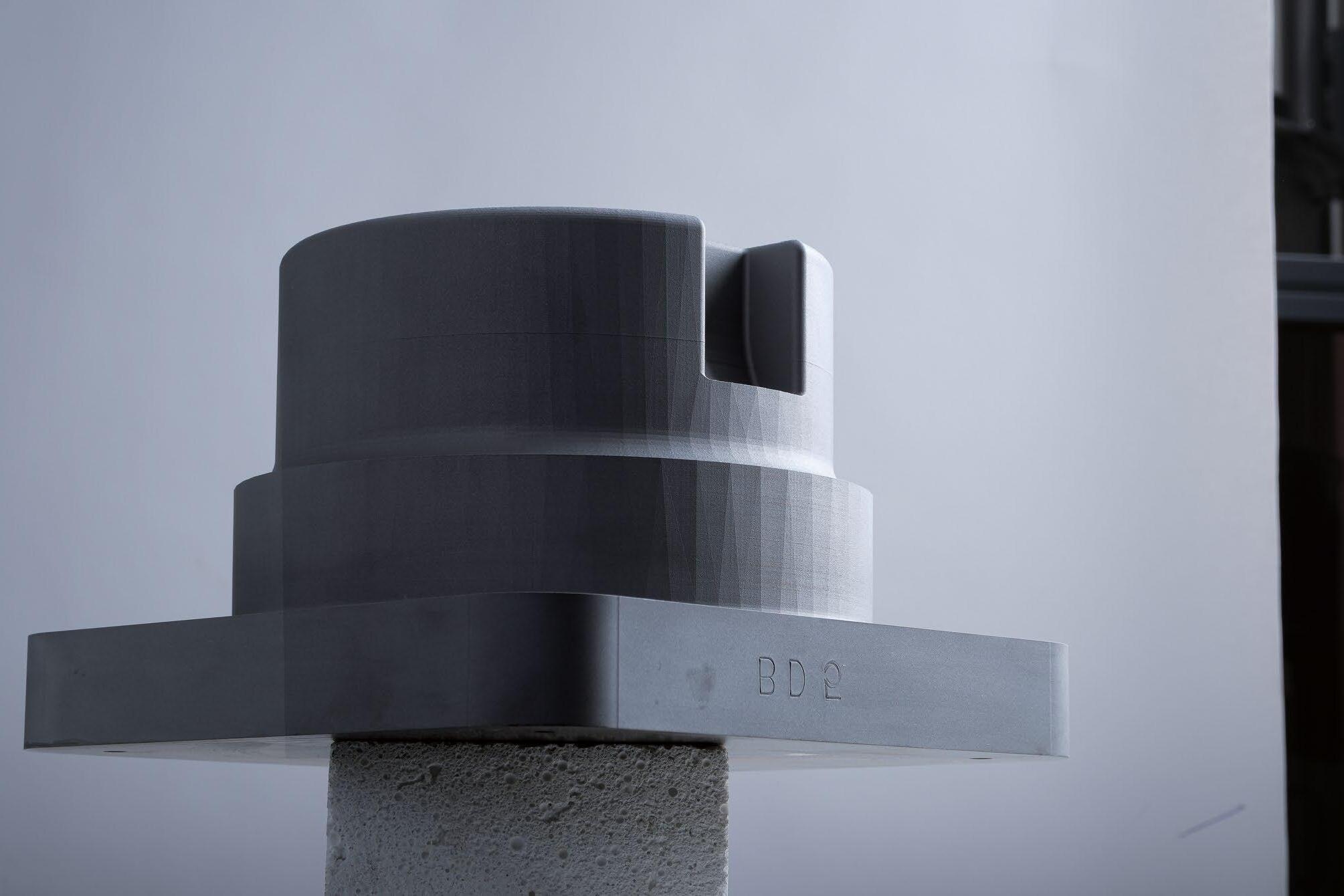
COBALT FREE METAL POWDER FOR AMDAP TM LT X C 0.25 Si 0.1 Ni 6 Cr 5.2 Mo 1.2 V 0.4
150×150mm WITHOUT CRACKING
OVER
https://www.daido.co.jp/en/products/powder/dap_am2/
6K Additive awarded $23.4M US DoD grant to expand critical metal upcycling
6K Additive, a division of 6K Inc based in Andover, Massachusetts, USA, has announced the initiation of a $50 million investment programme which will expand its current capacity and metal processing capabilities. The programme is supported by a $23.4 million grant awarded through the Office of the Assistant Secretary for Industrial Base Policy, through its Manufacturing Capability Expansion and Investment Prioritisation (MCEIP) directorate.
The agreement, entered into under Defense Production Act (DPA) Title III authorities, will help 6K Additive increase capabilities to upcycle high-grade metals – including titanium, nickel and refractory metals – used in alloys for aircraft structural components, turbine engine blades, rocket engines, radar systems, and many other critical
defence applications. In addition to doubling capacity, the programme will enable expansion in scrap sort, segregate, and processing, as well as the production of powder and remelt ingot to increase capability of domestic mill product capacity. The investment will support 6K Additive’s core efforts in facility renovation, talent acquisition, equipment installation, and engineering.
6K’s proprietary upscaling processes leverage abundant domestic sources of metal feedstock to include end-of-life components, machine-shop swarf, and scrap from manufacturing processes such as casting and forging. With MCEIP’s help, 6K expects to expand its capabilities and achieve full rate production at its Burgettstown, Pennsylvania, facility by the end of 2026.
“Our country’s national security relies heavily on materials used across numerous applications and controlling the supply chain from within the borders of the United States is paramount,” stated Frank Roberts, president of 6K Additive. “We are excited to announce this important expansion programme which enhances our capabilities to support our defence and commercial customer base.”
“The $23.4 million award from the DoD is a testament to the capabilities of 6K Additive for upcycling the most critical metals and alloys,” Roberts continued. “No other organisation has the history, experience, infrastructure or potential 6K Additive has in upcycling materials like titanium, nickel superalloys and refractory metals. We’re honoured to be selected for the award and recognise the trust the DoD has placed in our organisation.”
www.6kinc.com

Metal Additive Manufacturing | Spring 2024 82 © 2024 Inovar Communications Ltd Vol. 10 No. 1 | contents | news | events | advertisers | website | newsletter | Industry News
Tekna’s CA$20 million government funding plan extended
Tekna Holding ASA, Sherbrooke, Quebec, Canada, has announced the extension of a CA $20 million contribution agreement with the Canadian federal government’s Strategic Innovation Fund (SIF) programme. Under the terms of the reported amendment, the maximum amount to be disbursed remains unchanged at CA $20 million, however the programme has now been extended to March 2027. To date, CA $6.6 million has been disbursed.
“This amendment is a significant milestone, confirming Tekna’s position as an industry leader,” stated Luc Dionne, CEO of Tekna. “The extended support and enhanced financial framework under the SIF program are instrumental in driving forward our strategic initiatives. We
are committed to leveraging this opportunity to further our technological advancements and market leadership.”
The SIF programme aims to stimulate high-quality business investments across various sectors. It supports R&D initiatives that enhance technology transfer, commercialisation of innovative products, services, and processes, and encourages the growth of innovative firms.
“The SIF’s contribution has been pivotal in our growth journey,” added Espen Schie, CFO of Tekna. “The amended terms not only provide us with financial flexibility but also affirm the value of our ongoing projects. We are grateful for the support of Innovation, Science, and Economic Development Canada (ISED)
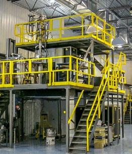
The
throughout the amendment process. This collaboration is a testament to our commitment to innovation and sustainable development in the advanced materials sector.”
www.tekna.com





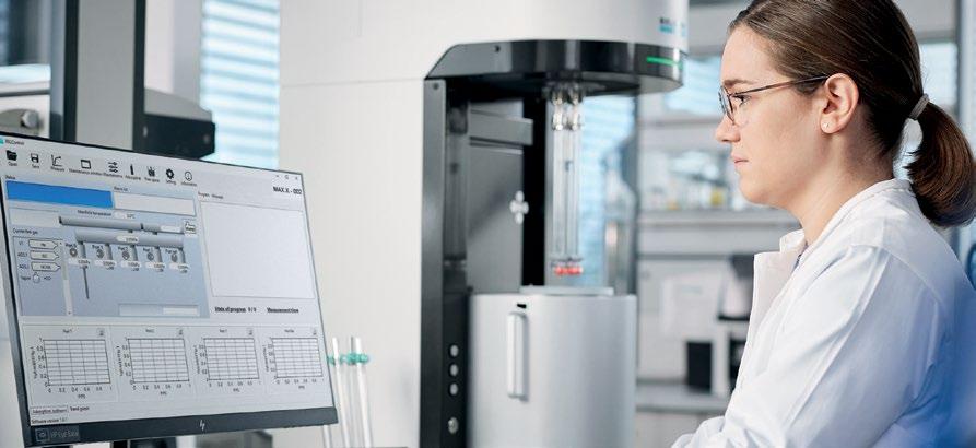
Metal Additive Manufacturing | Spring 2024 83 Vol. 10 No. 1 © 2024 Inovar Communications Ltd | contents | news | events | advertisers | website | newsletter | GETPDF Industry News www.microtrac.com PARTICLE CHARACTERIZATION OF METAL POWDERS Determine BET surface areas of metal powders quickly, accurately, and economically with MICROTRAC’s BELSORP MAX X Sorption Analyzer: I The specific surface area (m²/g) is an important parameter in the evaluation of metal powders regarding their processability. I Simultaneous measurement of up to 4 samples with high precision. I Rapid determination of BET surface areas with up to 12 analyses per hour - perfect for quality control of fine powders with high sample throughput. BELSORP MAX X SURFACE AREA AND PORE SIZE ANALYZER MRB-Advert-GB-PowderMet-175x120_neu.indd 1 15.02.2024 14:33:08
production of
company’s Teksphero-200 is designed for the large-scale
spherical powders (Courtesy Tekna)


Industry News While the world is busy imagining the future of Additive Manufacturing, Burloak is busy living it. Discover how Burloak is manufacturing complex parts at scale at burloaktech.com. ISO9001 certified NADCAP accredited ISO17025 certified CGP registered AS9100 certified ITAR registered Additive Manufacturing Services to Help You Scale
GKN Powder Metallurgy names JeanMarc Durbuis as new CEO
Dowlais Group plc has announced Jean-Marc Durbuis as the new Chief Executive Officer of GKN Powder Metallurgy. Durbuis joined the company on March 12, following the departure of Diego Laurent who served GKN for thirty-one years.
GKN Powder Metallurgy is a leading provider of powder metal materials, components, applications, and electrification solutions through its three business units, GKN Powders/Hoeganaes, GKN Sinter Metals and GKN Additive. In addition to GKN Powder Metallurgy, Dowlais Group is also the parent company of GKN Automotive and GKN Hydrogen.
“I want to thank Diego for his thirty-one years at GKN. He has achieved so much during this time at both GKN Powder Metallurgy and GKN Automotive. I am particularly grateful for all he has done to maintain GKN Powder Metallurgy’s position as one of the world’s leading suppliers of powder metal materials and sintered metal components,” stated Liam Butterworth, CEO of Dowlais Group Plc
Durbuis is expected to bring extensive commercial, operational
and leadership experience to GKN Powder Metallurgy as it positions itself for the transition to electric vehicles. Over the last twenty years, Durbuis has held several senior executive positions in the chemical sector, leading global teams in complex and demanding businesses. He has a proven track record across all operational functions and has been a member of several executive committees and boards.
Durbuis joins GKN Powder Metallurgy from Allnex, a global supplier of resins and additives to the coating and inks industry. He was the Executive Vice President of one of the Allnex’s global divisions with revenues of over €1 billion and was a member of the Allnex Executive Committee and Board of Directors. His achievements at Allnex include delivering improvements in his division’s financial and operational performance, and the delivery of significant M&A projects in different geographies.
“Given the critical role GKN Powder Metallurgy plays in solving complex challenges in the automotive and industrial markets, and the very
AMUK releases inaugural action plan to boost Additive Manufacturing ecosystem in the UK
Additive Manufacturing UK (AMUK), a trade association representing UK companies engaged in all aspects of the Additive Manufacturing value chain, spanning materials manufacture to post-processing of parts, has released its inaugural AMUK Annual Action Plan.
The plan details the current state of AM in the UK and outlines the specific steps that the trade association plans to take to address the challenges related to skills development, establishment of
standards, and optimisation of the UK supply chain.
The action plan establishes the member-set challenges and subsequent actions that AMUK will aim to undertake over the next 12 months. The three key challenge areas reported are:
• Supply Chain – Education, Adoption, Visibility and Qualification
• Skills – Education, Training and Recruitment

Jean-Marc Durbuis has been appointed as the new Chief Executive Officer of GKN Powder Metallurgy (GKN Powder Metallurgy)
exciting opportunities ahead for the business, I am delighted that JeanMarc will join us as the new CEO,” Butterworth added. ”He brings a wealth of experience that will enable the Powder Metallurgy team to capture the significant opportunities before it.”
Durbuis shared, “I am delighted to be joining GKN Powder Metallurgy as its new CEO. It is a world class business and will play a vital role in introducing new products to market, as we navigate the transition to EVs. I look forward to working with the team and meeting my new colleagues across the globe.”
www.gknpm.com
www.dowlais.com
• Standards – Roadmap, Testing, Certification, Inspection and Materials
Each of the challenges will undergo an annual assessment to determine if the actions taken are effectively driving forward the AM ecosystem in the UK.
Currently, the UK share of the global AM market is reported to be approximately 4% and valued at $690 million (£560 million). With the right support, input, and action to create an environment in the UK where Additive technology thrives, AMUK believes that the UK could capture almost 7% of the global market by 2030 which is expected to be in the range of $4billion to $6billion.
additivemanufacturinguk.org.uk
Metal Additive Manufacturing | Spring 2024 85 Vol. 10 No. 1 © 2024 Inovar Communications Ltd | contents | news | events | advertisers | website | newsletter | GETPDF Industry News
Researchers develop anti-fatigue titanium alloy using Additive Manufacturing
Researchers from the University of Science and Technology of China have published a study focused on increasing fatigue properties of additively manufactured metals in the journal Nature . As discussed in “High fatigue resistance in a titanium alloy via near-void-free 3D printing,” the team proposed a new strategy to create a titanium alloy via nearvoid-free Additive Manufacturing techniques.
According to the study, poor fatigue performance of additively manufactured materials under cyclic loading can result from the presence of microvoids.
Under the leadership of Prof Zhang Zhefeng and Prof Zhang Zhenjun from the Institute of Metal Research of the Chinese Academy of Sciences, the research team
developed an Additive Manufacturing process route to produce an almost void-free Ti-6Al-4V titanium alloy. This allowed the team to regulate microstructure and defects separately.
This Net-Additive Manufacturing Process (Net-AM) technique includes a Hot Isostatic Pressing (HIP) stage to eliminate the microvoids and subsequent high-temperatureshort-time heat treatment to restore the AM microstructure with fine martensite lath. This process has been successful in restoring a nearly void-free Net-AM microstructure to the titanium alloy.
The team confirmed that this void-free additively manufactured alloy has superior fatigue resistance compared to all other additively manufactured and forged titanium
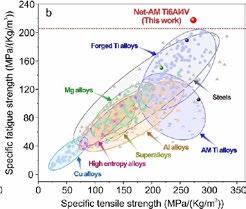
Evaluation of specific fatigue strength of the Net-AM microstructure in comparison with other microstructures (Courtesy Nature)
alloys, as well as other metallic materials.
“This research has revised people’s previous understanding of the low fatigue performance of 3D printing materials and is expected to advance such materials’ application in aerospace and other fields,” stated Zhang Zhefeng.
www.nature.com
en.ustc.edu.cn

Metal Additive Manufacturing | Spring 2024 86 © 2024 Inovar Communications Ltd Vol. 10 No. 1 | contents | news | events | advertisers | website | newsletter | Industry News
SWISSto12 reports €200 million backorders during year of growth
SWISSto12, based in Renens, Switzerland, has reported a successful business year in which the company secured a major contract with Inmarsat, doubled its team, opened new production facilities, secured financing and exceeded €200 million in customer backorders across its satellite and RF product businesses.
The company is developing the HummingSat, a new class of commercial GEO Smallsat that incorporates SWISSto12’s additively manufactured radiofrequency products and systems. The HummingSat will enable telecommunications operators to use assets that are lower in unit cost and more agile, whilst ensuring performance and reliability. The first HummingSat, developed in
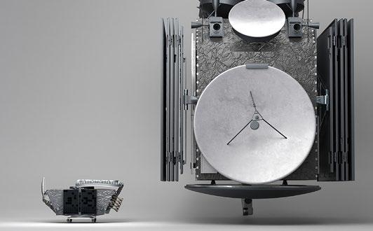
collaboration with the European Space Agency, is set to be launched by Intelsat in 2026.
Emile de Rijk, CEO of SWISSto12, shared, “2023 has been a landmark year for SWISSto12, demonstrating the strong interest of customers for our RF products and our new
class of small geostationary satellite: HummingSat. Looking ahead, we will aim to continue our growth as we position ourselves as a leading manufacturer of advanced satellite payloads and RF systems for the global aerospace market.”
www.swissto12.com



THE PERFECT CHOICE FOR CUTTING POROUS MATERIALS











Metal Additive Manufacturing | Spring 2024 87 Vol. 10 No. 1 © 2024 Inovar Communications Ltd | contents | news | events | advertisers | website | newsletter | GETPDF Industry News www.qatm.com Convenient TFT touch display Wide range of clamping accessories NEW Sample preparation of additive manufactured components is a challenging task, as the samples must be cut with as little deformation of the material as possible. With the new cooling system and precision guides, the Qcut 200 A offers the optimal conditions for these cuts Precision Cut-Off Machine I Precise and vibration-free cutting processes I Efficient coolant distribution I Automatic cleaning function I Optional flow monitoring for sensitive samples I New software functions for thin section applications
The HummingSat is a new class of commercial GEO Smallsat that incorporates SWISSto12’s additively manufactured RF products (Courtesy SWISSto12)
Kymera acquires Metallisation to expand thermal spray solutions
Kymera International, based in Raleigh, North Carolina, USA, has acquired Metallisation Limited, a thermal spray and automation technology company headquartered in Dudley, UK. Metallisation has been introducing metal spray equipment and consumables to the market since 1922.
The acquisition is expected to benefit both Metallisation and Kymera, with the companies
combining their relative strengths to become a global leader in thermal spray applications and solutions. It was added that Metallisation will contribute greatly to the continued growth of Kymera’s Surface Technologies business and its ability to deliver high-value, turnkey engineered solutions to global Tier 1 and OEM customers, specifically in the UK and mainland Europe.
Kymera International has acquired Metallisation Ltd, a thermal spray and automation technology company (Courtesy Metallisation)
“The acquisition of Metallisation aligns with our strategic initiatives and strengthens Kymera’s position in the thermal spray sector,” commented Barton White, CEO of Kymera. “We will now be able to provide our aerospace customers with a vertically integrated offering that includes equipment, materials and application services. This complete package will undoubtedly benefit the growth and adaptation of the company’s HaloJet™ product offering.”
Expert of Spherical Metal Powder
Standard Metal Powder
● Fe based alloys: SS316L, 17-4PH, 420, Maraging steel
● non-Fe based alloys: AlSi10Mg, In718, In625
Biomedicine powders
(Certificated by ISO 10993, ISO 13485)
● CoCrMo, CoCrMoW
● Ti6Al4V
Customized Metal Powder
● High Strength Stainless Steel : SS316LM (SS316L modified)
● Printable Aluminum Matrix Nano-composite (7075, 6061, 2024)
● Printable High Entropy Alloy(HEA/BMG powder)
The composition and particle sizes are adjustable.
Characteristics
High Purity
Excellent Sphericity
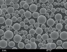
High Flowability Customization

Adam Shebitz, a Partner at Palladium Equity Partners, added, “The acquisition of Metallisation has compelling industrial as well as strategic logic. This investment represents an exciting opportunity to create value through vertically integrating surface technology materials and equipment with Kymera’s existing services business.”
This acquisition also expands Metallisation’s product offerings, enhancing its market positioning and growth opportunities.
Stuart Milton, Managing Director of Metallisation, shared, “We are extremely proud of Metallisation’s history and long-standing commitment to excellence in quality, customer service and engineering support. We have no doubt that under Kymera’s leadership, we will be able to not only continue offering great products and service to our customers, but also elevate our offerings and unlock significant growth opportunities. We are excited to be joining a team dedicated to innovation and collaboration.”
www.kymerainternational.com
www.metallisation.com


+ Ma d e in Ta iw a n Our Powder Will Power Your Business
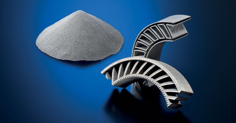
Superior corrosion resistance than UNS N10276
C01P
Corrosion resistant high-strength high entropy alloy (HEA)
C02P
Oil&Gas/Energy/ Semiconductors


Corrosion resistant HEA with improved toughness and creep resistance
C574P*
Higher hardness than Co - 6 alloy High strength maraging alloy
C21P
C01P
C02P
C574P*
High-strength superalloy
Oil&Gas/Energy/ Semiconductors Mold/Tooling Aerospace/Energy Aeros Semicon
YAG285AM1*
Lo - Cobalt maraging alloy
H44P (UNS N0
Mold/Tooling Aerospace/Energy


H05P
YAG350AM (Maraging 350) High strength maraging alloy
YAG350AM (Maraging 350)
YAG285AM1*
H718P (UNS N07718)
High-strength superalloy
H718P (UNS N07718) High-strength superalloy
H44P (UNS N06044)
H44P (UNS N06044) High
H05P
H05P
H713P
H713P (Modified Alloy713C)* Creep-resistant superalloy
H929P
H929P
R01P Highly Spherical W powder
L61P*
R02P*
ADMUSTER® series with wide & unique variations enable innovation in industries
Corrosion resistant Wear resistant Heat Resistant & Refractory Lightweight C W H R L
corrosion resistance than
C21P (UNS N06210) Superior
UNS N10276
high-strength high entropy alloy (HEA)
C01P Corrosion resistant
with improved toughness and creep resistance
C02P Corrosion resistant HEA
hardness than Co
6 alloy
C574P* Higher
-
strength maraging alloy
High
Cobalt maraging alloy
YAG285AM1* Lo-
High-temp corrosion-resistant Ni-Cr alloy
FeCrAl heat and oxidation resistant alloy
R01P Highly Spherical W powder R02P* Highly Spherical Nb powder
Aluminum 6061 based alloy
soon
Proterial, Ltd 2023 All rights reserved
Aerospace/ Semiconductors *Coming
©
ation in industries
r er
Lightweight L
© Proterial, Ltd 2023 All rights reserved
L61P* Aluminum 6061 based alloy Aerospace/ Semiconductors
n in indu
Corrosion resistant Wear resistant Heat Resistant & Refractory Lig C W H R
(UNS N06210) Superior corrosion resistance than UNS N10276
high
high
Corrosion resistant
-strength
entropy alloy (HEA)
with improved toughness and creep resistance
Corrosion resistant HEA
o - 6
Higher hardness than C
alloy
Lo - Cobalt maraging alloy
Ni- Cr
-temp corrosion-resistant
alloy
FeCrAl heat and oxidation resistant alloy
(Modified Alloy713C)* Creep -resistant superalloy
Highly Spherical Nb powder
L61P* Aluminum
soon © Proterial, Ltd Pr ote rial M e t a l Po w d e r ADMUS T E R ® s eri e s o v er v ie w innov ory R
*Coming
6044)
igh-temp
resist
Ni- Cr
H
corrosion-
ant
alloy
FeCrAl heat and oxidation
ant
resist
alloy
odified
Creep -resistant superalloy
Highly Spherical W powd
Highly Spherical Nb pow
eri e s o v er v ie w atio
R L 18) lloy 4) n- resist ant oy loy713C)* ralloy
H ighly S pherical W powder
H ighly S pherical N b powder L61P* Aluminum 60 61 based alloy rosp www.proterial.com
H713P (M
Alloy713C)*
H929P
R02P*
*Coming soon
Resis
R01P
R02P*
M&H adds SFM-AT1000-S powder removal system from Solukon
M&H CNC Technik GmbH, a provider of metal Additive Manufacturing design, development, production and finishing services based in Neudorf bei Ilz, Austria, reports it has installed an SFM-AT1000-S depowdering system from Solukon, Augsburg, Germany, at its facility.
The automatic powder removal system is specially designed for cleaning and post-processing additively manufactured parts. The SFM-AT1000-S can handle large and heavy metal components, with a height of up to 100 cm and a maximum weight of 800 kg.
“With the Solukon system, we can efficiently and thoroughly remove powder residue from complex parts with internal channels and cavities,” stated Patrick Herzig, M&H CEO. “This feature is a decisive advantage, as such complex geometries often present a challenge in post-processing and powder residues in the components could mean a loss of performance.”
The depowdering machine incorporates two rotating axes with servo drive, where the component moves along a programmable path. A built-in high-frequency
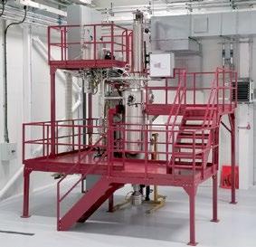
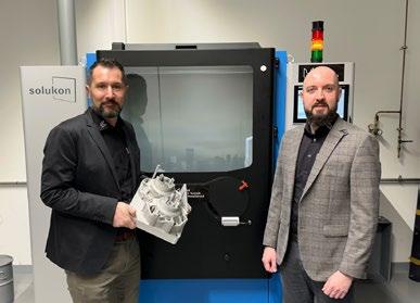
hammer also loosens powder clumps in particularly narrow channels. For reactive materials, the Solukon SFM-AT1000-S can operate under inert gas, providing maximum explosion and health protection.
“With the introduction of the SFM-AT1000-S, we are setting new standards in the post-processing of 3D printed parts in titanium, aluminium, stainless steel and materials such as Scalmalloy and Inconel. This technology enables us to further increase the quality of our products and make our production processes more efficient and even safer through series cleaning,” continued Herzig.
We can supply machines to atomize titanium alloys, super alloys, refractory and reactive metals, and ferrous and
alloys in high vacuum purged vessels with inert gas replacement atmospheres.
We have installed machines all over the world, from 1 kg research furnaces to 1000 kg production units.
www.arcastinc.com
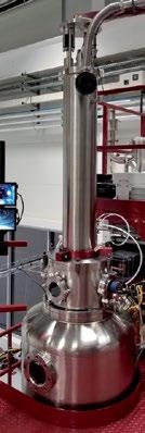
Andreas Hartmann, CEO and CTO of Solukon, added “The SFM-AT1000-S, sets new standards in the manufacturing industry – also thanks to its compatibility with our innovative SPR-Pathfinder software. With this unique software, individual motion patterns can be calculated automatically for each component based on the CAD file. By optimising and automating their post-processing procedures, we offer our customers – like M&H – a clear competitive advantage. With the Digital-Factory-Tool, a sensor and interface kit, our partners also have maximum transparency over the depowdering process,”
Post-processing for Formula 1 components
At M&H, the SFM-AT1000-S is used to post-process components for the aerospace and international motorsport industries, in particular Formula 1.
“The ability to clean components with extreme precision enables us to meet the specific and stringent requirements of these industries, where precision and reliability are particularly crucial. Using the SFM-AT1000-S from Solukon ensures that even the finest geometries can be reworked without compromising on quality,” emphasised Herzig.
www.solukon.de
www.mhcnc.com
Metal Additive Manufacturing | Spring 2024 90 © 2024 Inovar Communications Ltd Vol. 10 No. 1 | contents | news | events | advertisers | website | newsletter | Industry News Integrated InductIon alloyIng and atomIzatIon SyStemS
priced to meet
produce
quality, low cost, technically advanced metal powders fulfilling the requirements of today’s pioneering manufacturing processes.
Arcast Atomizers are custom built and competitively
the growing demand to
high
non-ferrous
M&H CEO Patrick Herzig (left) with Philipp Schwemberger, Head of Additive Manufacturing, in front of the new SFM-AT1000-SM&H at the company’s headquarters in Austria (Courtesy Solukon)
GKN Aerospace’s intermediate compressor case for Rolls-Royce UltraFan engine tested at full power
GKN Aerospace, a Rolls-Royce Core Partner in Clean Sky 2, has reported the successful testing of the UltraFan technology demonstrator incorporating the GKN-designed and manufactured Intermediate Compressor Case (ICC). The system was tested at full power at the Rolls-Royce facility in Derby, UK, with the initial phase of the test using 100% sustainable aviation fuel, underscoring a commitment to sustainable aviation practices.
Clean Sky 2 is a European aeronautics research programme dedicated to pioneering technologies aimed at reducing CO 2 emissions and aircraft noise levels. Funded by the EU’s Horizon 2020 programme and Europe’s aviation industry, Clean
Sky 2 aims to foster collaboration, global leadership, and enhanced competitiveness within the European aero industry.
The ICC is a critical structure between compressor modules and plays a vital role in carrying rotor loads to the engine casing and thrust mounts. GKN Aerospace’s developmental efforts encompass pioneering technologies – notably a low-cost, robust sectorised fabrication concept integrating castings. This process includes an advanced welding method based on precise computer simulations, optimised aerodynamics and acoustics for bleed system efficiency, a streamlined high curvature duct design, Additive Manufacturing of
attaching parts, and model-based design methods.
Henrik Runnemalm, Vice President of GKN Aerospace’s Global Technology Centre in Sweden, shared, “The successful ground testing of the UltraFan engine signifies a significant milestone for our ICC. It underscores the success of the Clean Sky 2 collaboration and showcases our incorporation of cutting-edge sustainable technologies, such as additive fabrication, in ICC development. We take immense pride in partnering with the Rolls-Royce team to contribute to this energy-efficient aero-engine of the future.”
GKN Aerospace has received substantial support in Sweden for developing innovative manufacturing processes for the ICC. This support comes from the Vinnova-funded IntDemo-project and the Västra Götaland Region.
www.gknaerospace.com
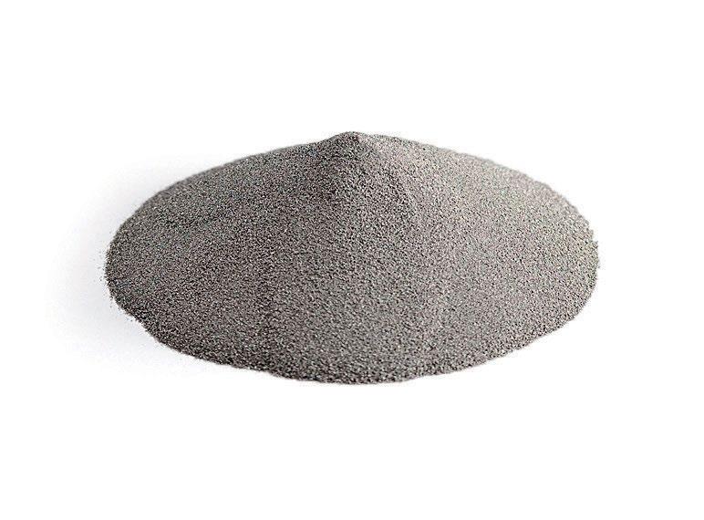
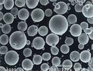
Metal Additive Manufacturing | Spring 2024 91 Vol. 10 No. 1 © 2024 Inovar Communications Ltd | contents | news | events | advertisers | website | newsletter | GETPDF Industry News
New method for Additive Manufacturing metal nanostructures using light
The research paper ‘Scalable Printing of Metal Nanostructures through Superluminescent Light Projection’ by Sourabh Saha, assistant professor in the George W Woodruff School of Mechanical Engineering, and Jungho Choi, a PhD student in Saha’s lab has been published in the journal Advanced Materials . The article discusses a new method for producing nano-sized metal structures using light, which is claimed to be 480 times faster and 35x cheaper than the current technology.
Manufacturing metal on the nanoscale, a technique known as nanopatterning, is reported to allow for the creation of unique structures with interesting functions. This is critical for the development of various technologies, such as electronic devices, solar energy conversion and sensors. However, it is generally believed that nanoscale Additive Manufacturing required highintensity light sources or a femtosecond laser, which could cost up to half a million dollars.
“As a scientific community, we don’t have the ability to make enough of these nanomaterials quickly and affordably, and that is why promising technologies
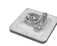
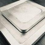
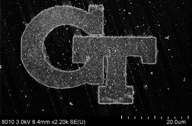
often stay limited to the lab and don’t get translated into real-world applications,” Saha stated. “The question we wanted to answer is, ‘Do we really need a high-intensity femtosecond laser to print on the nanoscale?’ Our hypothesis was that we don’t need that light source to get the type of printing we want.”
When looking for an affordable, low-intensity light that could be focused in a way similar to femtosecond lasers researchers turned to superluminescent light emitting diodes (SLEDs) due to their commercial availability. SLEDs reportedly emit light that is a billion times less intense than that of femtosecond lasers. Saha and Choi embarked on a mission to develop an original projectionstyle manufacturing technology, designing a system that converts digital images into optical images and displays them on a glass surface. This system works similarly to a digital projector but produces images that are more precisely focused.
The researchers utilised the distinctive characteristics of superluminescent light to produce highly precise images with minimal imperfections. Afterwards, they developed a clear ink solution consisting of metal salt and other chemicals to guarantee that the liquid could effectively absorb light. When light from their projection system hit the solution, it caused a chemical reaction that converted the salt solution into metal. The nanoparticles stuck to the glass’ surface, and the agglomeration of the metal particles creates the nanostructures. As the manufacturing process is projection-based, it can construct an entire structure at once, instead of in a point-by-point manner, making it much quicker.

After conducting tests, the researchers found that projection-style nanoscale manufacturing is achievable even with low-intensity light, as long as the projected images are sharply focused. Saha and Choi believe that their work can be easily replicated using commercially available hardware. This would be much more affordable than the femtosecond laser; the type of SLED that Saha and Choi used cost about $3,000.
www.me.gatech.edu
Metal Additive Manufacturing | Spring 2024 92 © 2024 Inovar Communications Ltd Vol. 10 No. 1 | contents | news | events | advertisers | website | newsletter | Industry News
www.indium.com/ MAMEZ 3D EZ Release™ Quick Release System for Metal 3D Printing PBF Part Removal Just Became Fast and Simple Release in SECONDS! • Designed for PBF (powder bed fusion) metal 3D printing • Parts printed on the 3D EZ Release print plate can be released in seconds • No EDM wire or other cutting saw is needed to remove the printed parts from the build plate • Separation is achieved by heating on a hot plate, or in a standard oven set to 200°C • Current 3D EZ Release™ plate size is 3.5" –different sizes and shapes are available upon request Contact our engineers: 3DPrint@indium.com ©2023 Indium Corporation
Scanning electron microscope image of additively manufactured silver Georgia Tech logo made with the SLP technique (Courtesy Jungho Choi/Georgia Tech)
FROM CONCEPT TO COMPONENT
The next dimension in tooling for the plastic injection moulding industry
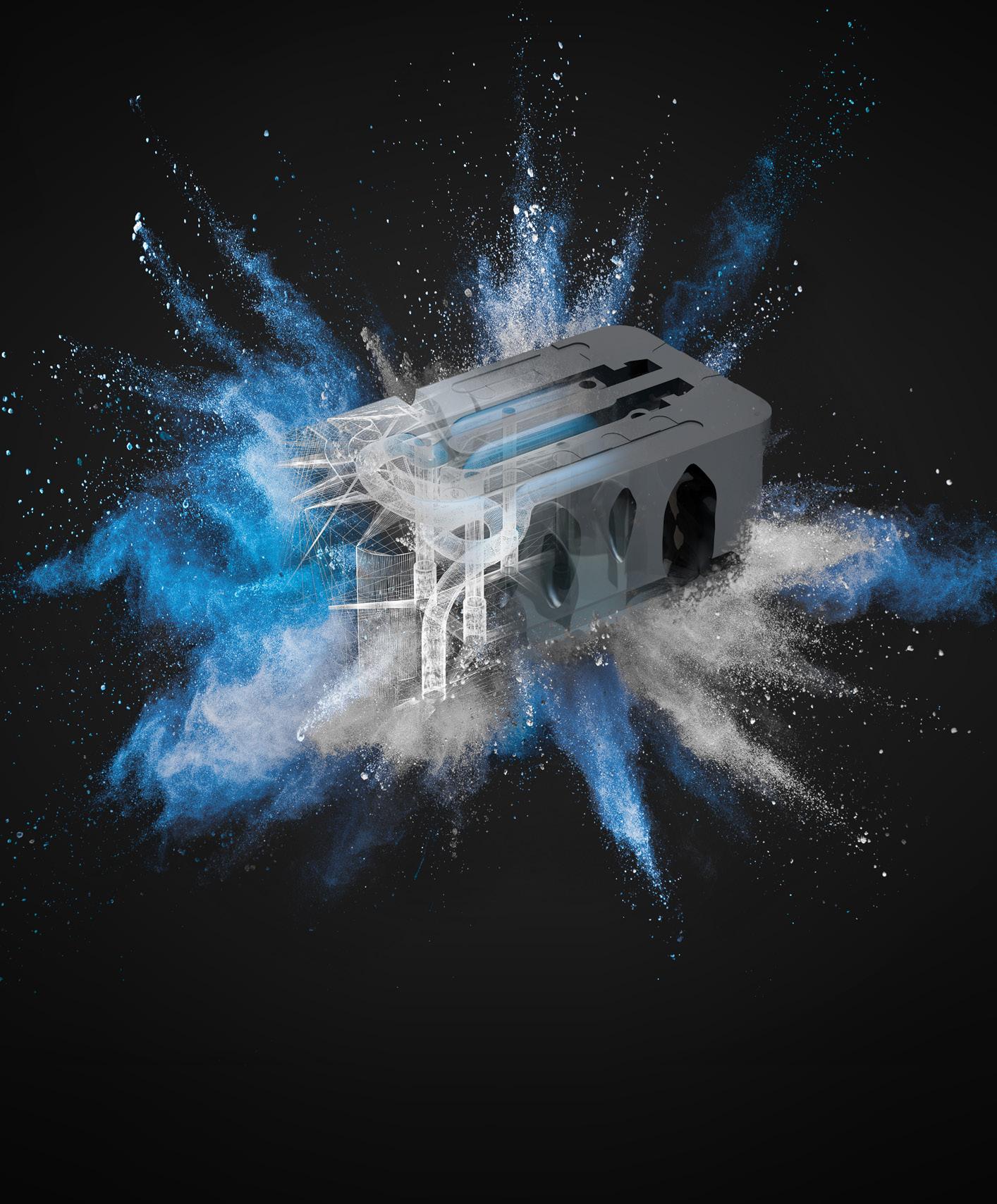
As a global steel and technology leader, we offer the full suite of production techniques and services throughout the value chain, supporting and driving innovation and development based on lengthy experience around materials and processing. Starting from the alloy development and metal powder production, to design and manufacturing and including post-processing. We offer the end-to-end solutions to reduce waste and mitigate risk in the supply chain with the goal of being your trusted and reliable business partner. We deliver tailormade solutions from concept to component.
voestalpine Additive Manufacturing
www.voestalpine.com/additive
ADDiTEC enters the world of motorsport through ADDiTEC Racing division
ADDiTEC, headquartered in Palm City, Florida, USA, has announced that it is entering the world of motorsport with the launch of ADDiTEC Racing. The company recently acquired race assets, including vehicles, support trailers and Additive Manufacturing machines, and is participating in the Porsche GT3 Cup Trophy and other related series events across the USA.
Central to ADDiTEC Racing’s mission is the greater integration of Additive Manufacturing in the motor racing sector. The company plans to utilise components manufactured with its Liquid Metal Jetting (a form of Material Jetting) and laser
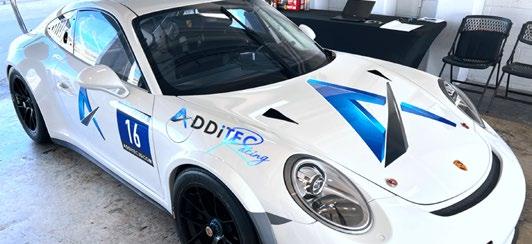
Directed Energy Deposition (DED) machines to showcase the capabilities and advantages of Additive Manufacturing for automotive parts.
“We believe that ADDiTEC Racing will not only showcase our technological prowess but also serve as a catalyst for accelerating our presence in the automotive sector,” stated Brian Matthews, CEO at ADDiTEC. “By competing at the highest level of motorsports and
Collins Aerospace purchases second NXG XII 600 from Nikon SLM Solutions
Nikon SLM Solutions AG, Lübeck, Germany, has announced that Collins Aerospace, an RTX business headquartered in Charlotte, North Carolina, USA, has purchased a second NXG XII 600 Laser Beam Powder Bed Fusion (PBF-LB) Additive Manufacturing machine for its facility in West Des Moines, Iowa.
Collins’ West Des Moines facility designs and produces engine components for commercial and military aircraft. In 2023, the company celebrated the opening
of a $14 million expansion of its Additive Manufacturing centre. The production-ready facility is one of nine in the US to receive the National Aerospace and Defense Contractors Accreditation Program (NADCAP) certification for Additive Manufacturing.
The new large-format NXG XII 600 machine will allow Collins to increase its AM production capacity at the site and expand the facility’s existing material capabilities to better serve its customers.
demonstrating the capabilities of our Additive Manufacturing solutions, we aim to raise awareness and drive adoption of our technology within the industry.”
ADDiTEC added that it plans to feature live Additive Manufacturing demonstrations at each race event, providing a firsthand glimpse of the possibilities for the automotive sector.
wwww.additec3d.com
www.additecracing.com
Sam O’Leary, CEO of Nikon SLM Solutions stated, “With the addition of Collins’ second NXG XII 600 printer, we’re fuelling their mission to revolutionise aerospace manufacturing. This not only empowers the industry as a whole but underscores our commitment to customer-driven innovation.”
The NXG XII 600 has a build envelope of 600 x 600 x 600 mm and is equipped with twelve 1000 W lasers, which the company claims make it up to twenty times faster than a single-laser system.
www.nikon-slm-solutions.com
www.collinsaerospace.com


Metal Additive Manufacturing | Spring 2024 94 © 2024 Inovar Communications Ltd Vol. 10 No. 1 | contents | news | events | advertisers | website | newsletter | Industry News
ADDiTEC has announced the debut of ADDiTEC Racing (Courtesy ADDiTEC)
Access all our back issues at www.metal-am.com
Cleaning
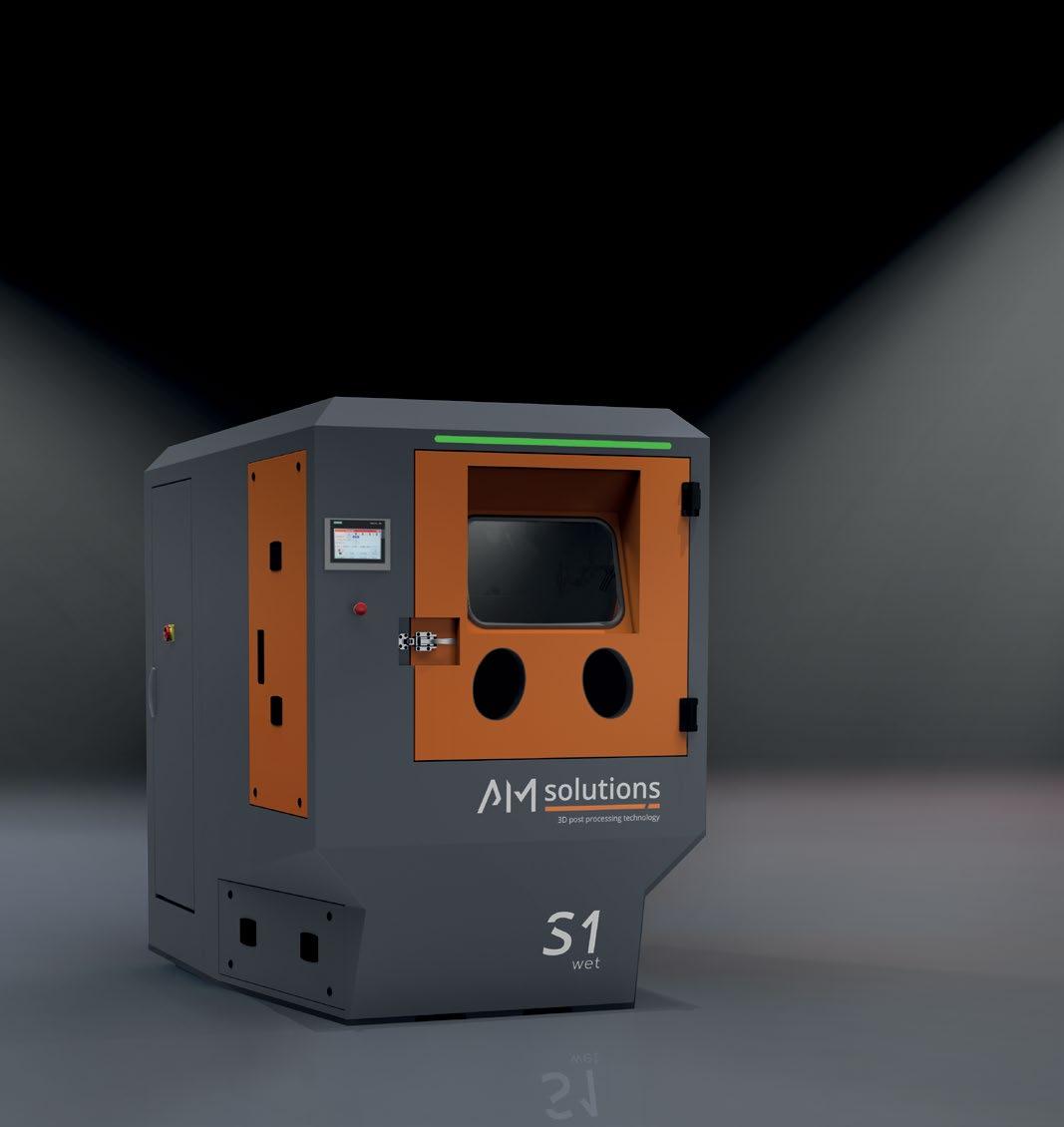
80 years of experience in surface finishing | Made in Germany
400 m² best in class test lab | Worldwide offices & service
Surface finishing
Polymers
Metal
www.solutions-for-am.com
S1 WET – THE VERSATILE WET BLAST SOLUTION FOR CLEANING AND SURFACE FINISHING
A brand of the Rösler Group
Materialise launches personalised temporomandibular joint arthroplasty replacement system
Materialise NV, headquartered in Leuven, Belgium, has launched its Personalised TMJ Total Arthroplasty System, a solution to treat patients requiring total temporomandibular joint (TMJ) arthroplasty. The solution combines implants, guides, and digital planning in an effort to streamline patient-specific TMJ treatment from a single company.
The TMJ is where the skull and jawbone meet, enabling the jaw to open and close. A clinical study with patients who have already received the personalised TMJ prosthesis showed improvement in their quality of life, pain levels, satisfaction, and eating ability compared to before
surgery, with accurate implant placement reported in 97% of cases. Furthermore, clinicians reported a 100% success rate for the TMJ system one year after the surgery within the same clinical study.
“Our TMJ Total Arthroplasty System provides a completely personalised solution. It allows the seamless transfer of the virtual preoperative surgical plan to the operation room, enabling the functional reconstruction of the temporomandibular joint,” shared Maarten Zandbergen, Market Manager CMF at Materialise. “This comprehensive solution offers clinicians full support for this complex procedure. It truly facilitates
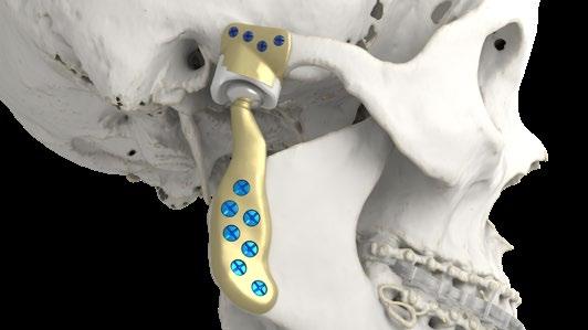
ORIX Rentec’s Tokyo 3D Lab expands offering with new BLT metal Additive Manufacturing machine
ORIX Rentec Corporation, a provider of engineering equipment and technology based in Tokyo, Japan, has expanded its range of Additive Manufacturing services with the addition of a new BLT-S320 metal Laser Beam Powder Bed Fusion (PBF-LB) AM machine from Xi’an Bright Laser Technologies Co., Ltd. (BLT), Xi’an, China.
Installed at Tokyo 3D Lab, the company’s Additive Manufacturing experience centre, the BLT-S320 can be used to process a wide range of materials, including titanium, aluminium, superalloys, stainless steel, high-strength steel, tool steel and copper alloy. It has a build area of 250 x 250 x
personalised treatment by providing a complete system including virtual planning software and clinical engineering support, as well as surgical guides, screws, and the implant itself.”
Materialise’s TMJ system is based on a fully digital process, enabling efficiency and accuracy based on the patient’s anatomy. The digitalised workflow starts with a patient’s CT scan and dental information. During an interactive online session, a Materialise clinical engineer supports the treating physician in surgical planning and device design. As soon as planning and device design has been finalised, Materialise manufactures the personalised TMJ implant in its facilities, providing the surgeon with implants and instruments for surgery. The entire solution is sourced from Materialise, making it compatible with the company’s full personalised cranio-maxillofacial (CMF) solutions and expanding access to personalised treatment.
“Our implants, instruments, 3D planning technology, and clinical support empower surgeons as they strive to achieve precise and reliable outcomes,” said Martijn Orye, CMF Market Specialist. “Personalised solutions are becoming the primary choice for more challenging or complex cases such as TMJ replacements. Our complete solution streamlines and speeds up what used to be a slow personalisation process with other providers.”
www.materialise.com
400 mm and is powered by two 500 W lasers.
Opened in 2015, the Tokyo 3D Lab centre offers an introduction to metal Additive Manufacturing and provides customers with first-hand experience and support. In addition to the new BLT machine, Tokyo 3D Labs has an EOS M290, a Trumpf TruPrint1000 and a Metal X from Markforged. It also has a selection of polymer AM machines and post-processing services.
www.orix.co.jp/grp/en
www.xa-blt.com/en
Metal Additive Manufacturing | Spring 2024 96 © 2024 Inovar Communications Ltd Vol. 10 No. 1 | contents | news | events | advertisers | website | newsletter | Industry News
Materialise has launched its Personalised TMJ Total Arthroplasty System, a solution to treat patients requiring TMJ arthroplasty (Courtesy Materialise)
Navigation and Support
In a complex industry, we’ll guide you the entire way.
We’ve got one mission, to support as many metal part makers in the MIM and Metal AM industry as possible. Our team of processing experts utilize 20+ years of experience to share all our knowledge and help you overcome challenges, develop better processes and become successful part makers. We help develop real world, practical solutions based on many lessons learned along our journey. Being the ONLY debind and sinter service provider with full sized production equipment, we are honored that we have been able to support every industry currently utilizing MIM and Metal AM. DSH is the only source for the best process support, toll processing and educational resource for your MIM and Metal AM applications.
We offer:
Remote Process Engineering, Small/Large Toll Processing, R+D projects, Educational Support on Total Process Management.



Metal Additive Manufacturing | Spring 2024 97 Vol. 10 No. 1 © 2024 Inovar Communications Ltd
Partner in MIM/AM
Your
107 Commerce Road | Cedar Grove, NJ 07009 USA | +1 973.239.7792 | dshtech.com
Authentise awarded US government funding for cybersecurity in Additive Manufacturing
Authentise, based in Philadelphia, Pennsylvania, USA, has been chosen as one of ten projects selected for funding by the US Department of Energy in collaboration with the Cybersecurity Manufacturing Innovation Institute (CyManII). The selected projects have been awarded a total of $4.8 million in research and
development funding and are aimed at strengthening cybersecurity in the US manufacturing sector.
Authentise was awarded $573,710 to build a secure real-time measurement system specifically to detect if malicious third parties have infiltrated an Additive Manufacturing system to adjust or introduce
defects, which would otherwise be undetectable during manufacture. Partnering with Addiguru, i3DMFG, and CyManII, this team will demonstrate multiple verification data streams based on the digital model build file, all integrated into the CyManII-developed CyberPhysical Passport. This system not only looks to improve cyber security, but also aid AM manufacturers in their ability to improve manufacturing quality assurance approaches and workflows.
www.authentise.com
amace Solutions





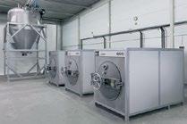
expands production capacity with move to larger Additive Manufacturing facility
amace Solutions Pvt Ltd, a company of the Ace Micromatic Group (AMG) based in Bangalore, India, has recently relocated to a new dedicated Additive Manufacturing facility. The move has resulted in a significant increase in production capacity, providing approximately five times more floor space than at its previous site.
amace offers a range of metal Additive Manufacturing machines, including the STLR-400 launched in 2021, and the smaller STLR-180. The company also offers a range of metal powders and additional services.
In addition to increasing its production capacity, the new facility will enable services such as advanced AM labs for new material and parameter development, a large repository of spare parts and added competencies for application support. The company is also expecting to expand its workforce. www.am-ace.com
Metal Additive Manufacturing | Spring 2024 98 © 2024 Inovar Communications Ltd Vol. 10 No. 1 | contents | news | events | advertisers | website | newsletter | Industry News

Mark Benedict awarded Military Additive Manufacturing Lifetime Achievement award
Dr Mark Benedict, Additive Manufacturing lead for the Air Force Research Laboratory’s (AFRL), Materials and Manufacturing Directorate and chief technical advisor at America Makes, has been announced as the 2023 recipient of the Military Additive Manufacturing (MILAM) 3D Printing Lifetime Achievement Award. The award is granted for the consistent, distinguished service of an individual or group, and for making groundbreaking lifetime contributions

Dr Mark Benedicta is the 2023 recipient of the Military Additive Manufacturing Lifetime Achievement Award (Courtesy Jonathan Taulbee)
with an enduring impact in the areas of Additive Manufacturing across the Department of Defense.
“We’re tremendously proud to have Mark on our team,” said Dr Charles Ormsby, AFRL division chief, Manufacturing and Industrial Technologies. “He is truly a world leader in Additive Manufacturing technology who transformed a research tool into a competitive advantage for our warfighters. I can’t think of anyone more deserving of this recognition.”
“He immediately came and visited us for a deep-dive technical kickoff, bringing with him an immense curiosity and a wealth of experience,” Dr Blake Teipel, CEO of Essentium Inc., who nominated Benedict for the MILAM award, commented. “I couldn’t be more delighted that Dr Benedict received this well-deserved award. His longstanding tenure as a thoughtand technology-leader not only within the United States Air Force and AFRL communities, but also for the entire Additive Manufacturing industry, is well-known.”
Benedict attended the University of Dayton, where he earned his Bachelor of Science in chemical engineering. It was during this time that he began working at AFRL in the manufacturing research branch. He then went on to attend Wright
Addiblast introduces MARS02 BJP for Additive Manufacturing depowdering
Addiblast, based in Dolenjske Toplice, Slovenia, has introduced its MARS02 BJP depowdering machine, a solution which aims to remove powder from challenging areas of additively manufactured parts. The MARS02 BJP comes with a custombuilt box that can accommodate parts up to 700 x 450 x 250 mm,
making it suitable for a wide range of projects.
The MARS02 BJP can handle a variety of materials, including steel and titanium – for which it has an explosion-proof, airtight environment – and ceramics. The machine is equipped with a loading plate that can be customised to fit the
State University through a DAGSI scholarship, where he earned his Bachelor’s and Master of Science degrees in material science. He continued to work at AFRL during this time, and eventually earned his doctorate in metallurgy and material science from Cambridge University.
During his time at AFRL, Benedict has worked on various projects but said that the Pacer Edge programme, which was run by the Air Force Lifestyle Management Center (AFLCMC) engines group, and his work on the acceleration of largescale Additive Manufacturing were two highlights.
About six years ago, Benedict transitioned to the role of chief technical advisor at America Makes, which he said involved more investment planning and strategic alignment of resources with future Air Force needs, maturing the technology and getting it to airworthy status.
Among other awards and honours Benedict has received, he was named an AFRL Fellow in 2023. This honour represents 0.3% of the AFRL professional technical staff and has only been granted to 251 AFRL recipients since the programme began 37 years ago. Benedict is also the recipient of the 2020 Director’s Award (Senior Individual), and the 2023 Director’s Award (Team) as part of the Hypersonics Team. Benedict was recently named Senior Scientist, Convergent (Digital) Manufacturing, at AFRL.
www.afresearchlab.com
client’s build box. It also has a lifting mechanism that allows movements in the z-direction up to 300 mm, which is controlled with pedals and has two limit switches.
There are also two optional capacities available: an upgraded recycling system, which integrates sieving capabilities into the machine, and an inert gas fusion system, which is equipped with openings and built-in gloves.
www.addiblast.com
Metal Additive Manufacturing | Spring 2024 100 © 2024 Inovar Communications Ltd Vol. 10 No. 1 | contents | news | events | advertisers | website | newsletter | Industry News
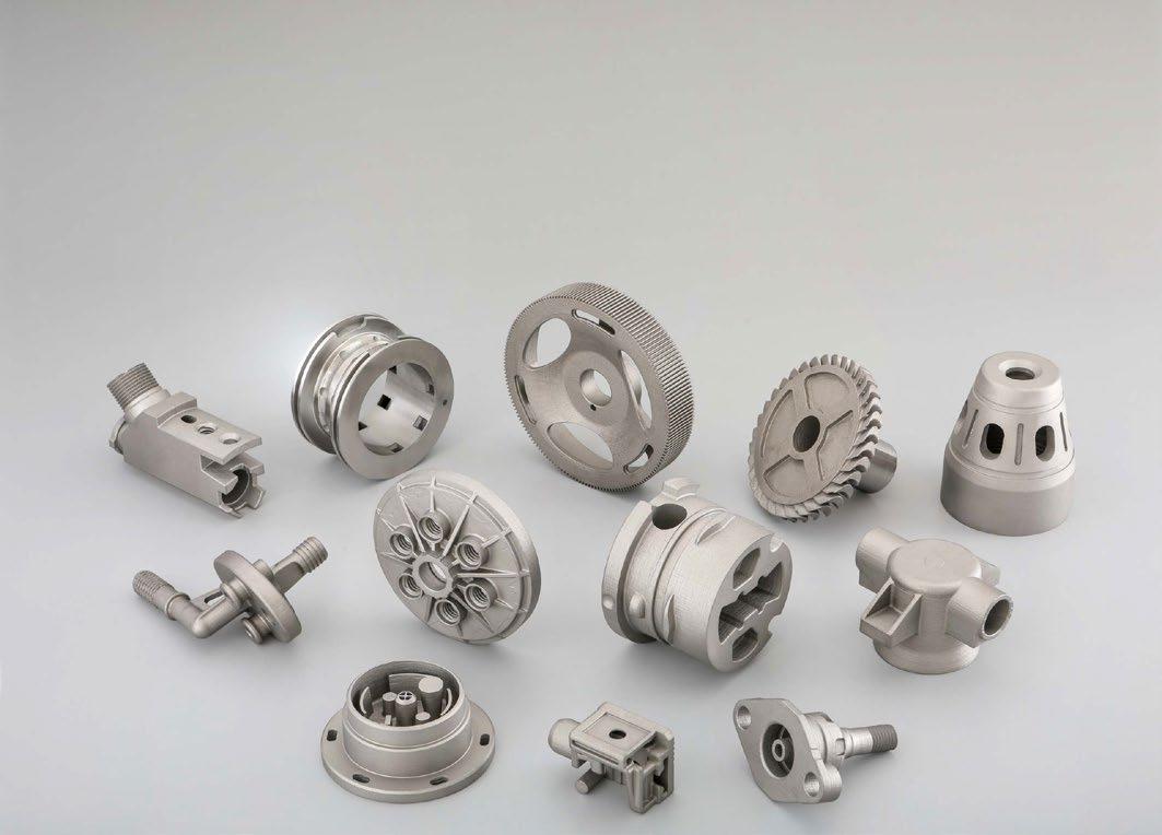
LOOKING FOR PROTO-SAMPLES IN 15 DAYS ? www.indo-mim.com ISO 9001:2015 / IATF 16949:2016 / AS 9100:Rev D / ISO 13485:2016 / ISO 14001:2015 NORTH AMERICA Email: Mukund.N@indo-mim.com Ph: +1 (210) 557-1594 EUROPE Email: InfoEU@indo-mim.com Ph: +49 1732656067 ASIA Email: InfoHQ@indo-mim.com Ph: +9198459 47783 / +91 98450 75320 CONTACT FOR MORE DETAILS ~ 300 grams max, Footprint equivalent of baseball size or less, 0.02” (0.50 mm) wall thickness minimum Material Options (Metal) Material Options (Ceramics) Build Envelope Quantity Tolerance capability 17-4PH, SS 316, Tool Steel M2 & S-7, Inconel 625, 4140 Alumina 99.5%, Zirconia 10~50 samples based on footprint. Larger quantities up to 1,000 pcs welcome depending on the part size. Within 2% of the feature size, 2~3 Ra Surface finish, Option of finishing to closer tolerances available. 3D PRINTING IS YOUR SOLUTION LPBF Binder-Jetting Ceramic NPJ Metal/Ceramic SLA
Retech’s new integrated plasma gas atomiser for cheaper titanium powders
LE-237iR 2024-1a.ps
T:\MISC\ADS\LE-237\LE-237iR 2024-1a.cdr
Tuesday, March 5, 2024 11:22:49 AM Color
profile: Disabled
Retech, a division of the Seco/ Warwick Group based in Swiebodzin, Poland, and with facilities in New York and California, USA, has announced the development of an integrated plasma gas atomiser (PGA) that is claimed to achieve atomisation rates greater than 10x the rate of currently-available technologies. The integrated system utilises Plasma
Arc Melting (PAM) technology, in combination with gas atomisation, to process a wide variety of refractory and reactive alloys, amorphous metals, or superalloys. The atomiser can use most feedstock formats –including sponge, compacts, recycled scraps and ingots – and enables continuous processing via an airlock feeder system that doesn’t interrupt
melting to recharge. The atomiser also eliminates nozzles, which can be prone to clogs, thus improving reliability and simplifying cleaning and product changeover.
“At Retech, we are too busy commissioning new furnaces, and trusted by customers with too many trade secrets and defence clearances, to be able to boast of our accomplishments much, so it is a delight to have a new innovation in PGA that we can shout from the rooftops!” stated Earl Good, Retech’s Managing Director and President.



While the company’s suite of melting technologies is capable of melting a wide range of reactive and refractory elemental metals and alloys, the economical production of titanium powder, in particular, offers great potential. Retech is seeing growing interest in titanium use, with companies finding ever more applications for the metal. This is boosted by the perceived prestige of using titanium, even in consumergrade products that don’t actually require it, such as cell phone cases, watches, etc.
To support the growth of Retech’s PGA technology, parent company Seco/Warwick Group secured a $10 million subsidised loan from the Polish Foreign Expansion Fund 2 FIZ AN, which offers companies co-financing of their foreign investment projects.
“This dovetails perfectly with our recent membership in America Makes, the National Additive Manufacturing Innovation Institute,” added Good.
“Sure, I look forward to what the big players will do with the less expensive powder metals Retech will enable, but they already have access to the material and technology, but what really excites me is the opportunity to see what creative young minds can do with this once Retech makes it accessible enough that they can afford to have fun with Ti AM in a garage-tech sense. Take bold steps without fear of mistakes. It is not so much about making the existing tech less costly, the excitement is in the fields where titanium will become a feasible option, where it was not before.”
www.secowarwick.com
www.retechsystemsllc.com
Metal Additive Manufacturing | Spring 2024 102 © 2024 Inovar Communications Ltd Vol. 10 No. 1 | contents | news | events | advertisers | website | newsletter | Industry News

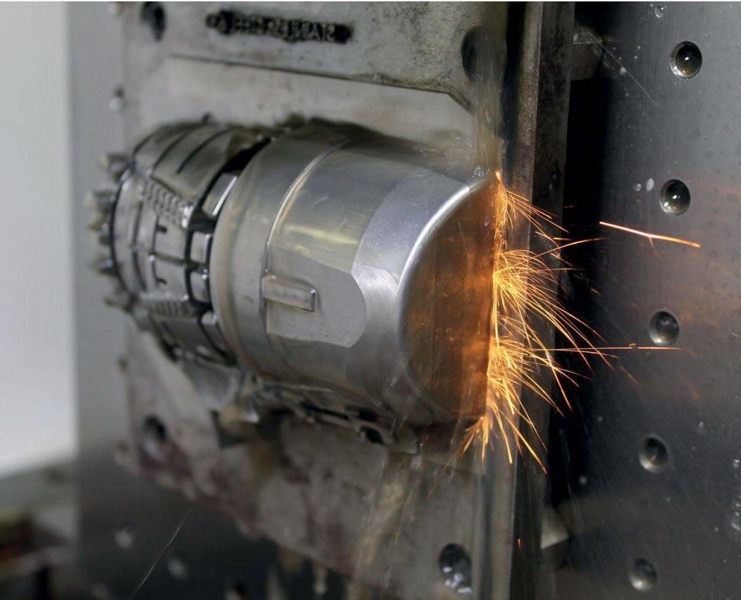
400x320x280
400x320x410
400x320x410
1000x800x800
1000x800x1050
630x500x625
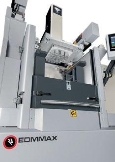
400x400x300
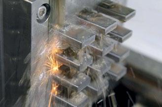
433W
434WW
434W
818W
1800W
656W
45HW Made in Taiwan
EDMMax
EDMMax
EDMMax
EDMMax
EDMMax
EDMMax
FC
mm (x,y,z axis) - 4 axis Max. workpiece Wt: 600kg . 1320 lbs
mm (x,y,z axis) - 4 axis Max. workpiece Wt: 600kg . 1320 lbs Uses pure waterno additives! Horizontal submerged cutting Horizontal submerged cutting
mm (x,y,z axis) Max. workpiece Wt: 3000kg . 6600 lbs
1100x1400x1250
mm (x,y,z axis) - 4 axis Max. workpiece Wt: 600kg . 1320 lbs
mm (x,y,z axis) - 4 axis Max. workpiece Wt: 2000kg . 4400 lbs
mm (x,y,z axis) - 4 axis Max. workpiece Wt: 2000kg . 4400 lbs
mm (x,y,z axis) Max. workpiece Wt: 100kg . 220 lbs
mm (x,y,z axis) - 4 axis Max. workpiece Wt: 1000kg . 2200 lbs EDMMax “Fast” Wire EDMs EDM Network offers “Everything in EDM” affordably priced! (Moly) (630) 466-5588 | 17974 Bucktail Ln, Sugar Grove, IL 60554 info@edmnetwork.com
1100HW www.edmnetwork.com
EDMMax
Velo3D launches Flow Developer to enhance control in AM
Velo3D, Inc., headquartered in Campbell, California, USA, has announced the release of Developer, a new offering made available in the company’s Flow build preparation software that enables full transparency and control of the parameters used in the Additive Manufacturing process.
Developer is available for users of Flow 7.0, the latest version of Velo3D’s build preparation software that turns traditional design files into build files. Developer grants editor-level access to build parameters, giving companies maximum flexibility and control when working with their Velo3D Additive Manufacturing solution. With this access, users can import the proven parameters that they have developed, optimise default parameters for specific application needs, and develop parameter sets supporting new material development for novel solutions and specific applications.
Prior to its general release, Developer was made available to select customers for feedback, including Ursa Major, a privately funded company developing rocket propulsion technology. During this phase, engineers have been able to directly transfer their custom parameters into their Velo3D solutions. The Developer software is reported to have enabled early-access customers to easily increase their production of parts as their applications progressed from development to production.
“It can be a challenge to produce repeatable results across different metal 3D printers — even when they’re the same model of printer — however, Velo3D’s solution can consistently produce parts within spec across any of its printers, which provides huge benefits for companies looking to scale production of their parts,” said Thomas Pomorski, Additive Manufacturing Manager at Ursa Major. “When our team first tested
Ipsen celebrates 75th anniversary with record revenue and growth
Ipsen, headquartered in Cherry Valley, Illinois, USA, celebrated its seventy-fifth anniversary in 2023. In this milestone year, the company also achieved several significant accomplishments, including record revenue and substantial growth.
In 2023, Ipsen shipped more than fifty vacuum furnaces to customers across ten countries, demonstrating its international reach across a diverse userbase. Ipsen also reported exceptional performance in the aftermarket sector, where it achieved a 38% increase in replacement hot zone orders for both Ipsen and non-Ipsen furnaces compared to its previous record year.
Due to the increasing demand, Ipsen repurposed its former ceramics facility to expand hot zone production capacity.
Additionally, Ipsen completed ISO/IEC 17025:2017 accreditation for pyrometry services, ensuring its adherence to the highest industry standards. Ipsen also conducted calibration and temperature uniformity surveys costing over $1 million.
Recognising the growing service needs of the industry, Ipsen made significant investments in its workforce during the year. The company hired over sixty new employees in 2023 and established a dedicated team for recruiting
Flow Developer, we transferred parameters we developed on a non-Velo system, hoping we could easily produce the same part on Velo3D’s system and then take advantage of the scalability it provides.”
“On our first try, we imported a part with highly complex, sensitive features and achieved incredible results that were within specification. Since then, we’ve accomplished the same process with other parts and in some cases, have been able to reduce print time by nearly 50% without sacrificing accuracy or quality,” he concluded.
Flow is intended to act as a key part of Velo3D’s integrated approach to Additive Manufacturing which works to enable machine-tomachine consistency. In addition to Flow and the Sapphire family of AM machines, the company’s solutions also include Assure quality assurance software, which monitors a build layer-by-layer to ensure consistent geometric accuracy, surface finish, and material properties throughout a finished part.
www.velo3d.com
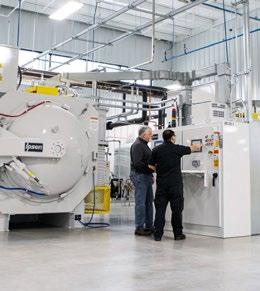
Ipsen celebrated its 75 th anniversary with a year of record revenue and growth (Courtesy Ipsen)
and training field service engineers in order to further grow its service presence.
www.ipsenglobal.com
Metal Additive Manufacturing | Spring 2024 104 © 2024 Inovar Communications Ltd Vol. 10 No. 1 | contents | news | events | advertisers | website | newsletter | Industry News



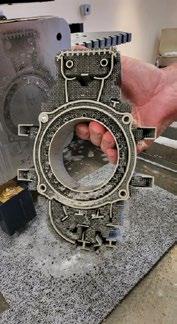



TAKE A DEEP DIVE INTO THE TECH & MACHINE ADVANTAGES Trusted by OEM Metal AM Manufacturers Nationwide Service and Support Free Test Cut / Time Studies Available Contact Our Reps For Metal AM Part Removal Economic Powerful Molybdenum wire has nearly double the tensile strength and a 3x higher melting point than brass. It makes challenging cuts a breeze! Exclusive Fully cast robust machine structure with unparalleled accuracy and reliability not found in other fast-wire EDMs. information@edmperformance.com #1 Solution Accurate & Cost-Effective HB Moly Cut Wire EDM These powerful machines run for approximately $1.00-$2.00 per hour with all parts, consumables, and electricity accounted for! West Coast: 1-800-336-2946 information@edmperformance.com Midwest/East Coast: 1-800-511-5532 EDMperformance.com 600mm+ Build Platform Capable! West Coast: (800) 336-2946 East Coast / Midwest: (800) 511-5532 MOLYCUTEDM.COM OR SCAN THE QR CODE BELOW
BMW uses its automotive expertise for Additive Manufacturing of custom bobsleigh shoe spike plates
As technology partner of the German Bobsleigh, Luge, and Skeleton Federation (BSD), the BMW Group is utilising its Additive Manufacturing expertise, gained from the development and manufacturing of automotive components, to create high-performance customised spike plates for shoes that will be used in the 2026 Olympic Winter Games.
In conventional bobsleigh shoes, defined rows of nails are permanently attached to the toe area of the soles. These nails cannot be replaced or moved, meaning that once the nails have worn out, the shoe needs to be replaced. The solution that BMW and the BSD are working on is based on track and field shoes, for which threads for screw spikes are used to attach spike plates on which the spike nails can largely be distributed without restriction.
This adaptation combines several advantages, including a wider selection of shoe styles. Further, the material and geometry of the plate, as well as the placement of the spike nails, can be used to vary the rigidity and, above all, the power transmission to the ice. With respect to individual running styles as well as the different running paths that the various positions entail – especially in a four-man bobsleigh – this enables better acceleration than standard spikes could ever make possible.
In practice, this means that customised spike plates have to be designed and manufactured for each athlete, which makes Additive Manufacturing an obvious choice.
“We have been using 3D printing to make components for prototypes, customised one-offs, as well as for series production for more than thirty years,” stated Claudia Rackl, BMW Group Additive Manufacturing Projects & Qualification. “The major advantages of 3D printing are the time and cost savings as well as
a high degree of flexibility. This allows us to quickly manufacture, test and efficiently optimise different variants.”
The geometry of the spike plates is developed using software and automatically aligned with the topography of the individual shoes, which is recorded by a 3D scanner. The spike plates are then additively manufactured using a Laser Powder Bed Fusion (PBF-LB) process.
Various alloys and geometrics are currently being tested and
refined. Once the basic parameters have been determined, software is used to automatically adapt the design of the spike plate to any type of shoe, any shoe size, and any number of attachment points on the sole of the shoe. It will also be possible to produce special spike plates for the individual requirements of athletes or even for different weather and ice conditions.
“We tested the spike plates in the World Cup and received a lot of positive feedback from the athletes,” added bobsleigh head coach René Spies. “Nevertheless, a few tweaks are still necessary here and there, but we expect to have the perfect shoes to compete in by the 2026 Olympic Winter Games at the latest.”
www.bmwgroup.com
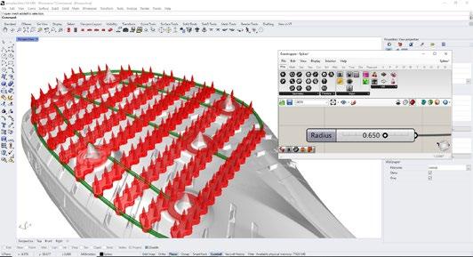
Metal Additive Manufacturing | Spring 2024 107 Vol. 10 No. 1 © 2024 Inovar Communications Ltd | contents | news | events | advertisers | website | newsletter | GETPDF Industry News
The geometry of the spike plates is developed using software and automatically aligned with the topography of the individual shoes (Courtesy BMW)
A batch of additively manufactured customised spike plates developed for the German Bobsleigh, Luge, and Skeleton Federation (Courtesy BMW)
Additive Manufacturing plays pivotal role in Land Space’s ZQ-3 reusable rocket
Additive Manufacturing technology provided by Bright Laser Technologies (BLT), Xi’an, China, has played a pivotal role in the success of recent vertical takeoff and landing tests conducted by Land Space’s ZQ-3 VTVL-1 reusable rocket. The tests proved the viability of Land Space’s design for the recovery
of its liquid oxygen-methane rocket’s first stage, which features a number of metal AM components.
Land Space, a private space launch provider based in Beijing, first partnered with BLT in 2019 when it recognised the possibility of metal Additive Manufacturing

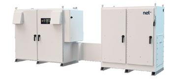

Bright Laser Technologies (BLT) played a pivotal role in the successful recovery test of Land Space’s ZQ-3 VTVL-1 (Courtesy BLT)
for the production of rocket components.
Additive Manufacturing was used to produce a number of components in the rocket, including joint elements, igniter mounts, and the intricate casing section which featured a complex internal cooling structure. These components posed challenges in traditional metal fabrication methods, including prolonged production cycles, difficulties in mould manufacturing, and escalated costs. Leveraging metal Additive Manufacturing capabilities not only streamlined the manufacturing process but also resulted in significant cost savings and reduced development timelines.
Land Space commented, “To better meet the technical demands of our engine, we chose metal 3D printing technology for the production of critical components with exacting quality standards. Recognising BLT as a frontrunner in additive technology solutions, and excelling in metal 3D printing services, equipment, and powders, we decided to cooperate with BLT. BLT played a crucial role in reducing production time, expediting deliveries, and supporting our rapid development iterations. Land Space commends the partnership with BLT and anticipates further collaboration with BLT in aerospace.”
www.xa-blt.com
Metal Additive Manufacturing | Spring 2024 108 © 2024 Inovar Communications Ltd Vol. 10 No. 1 | contents | news | events | advertisers | website | newsletter | Industry News MAM Island Half Page Ad – Grow Profits – C Series.indd 1 12/7/22 11:38 AM













Outstanding performance
Special stainless steels, nickel and cobalt alloys produced by VDM Metals are used in many of today‘s key technologies for the safe and reliable handling of corrosive and high-temperature processes and procedures. In addition to exceptional materials, available as powder for additive manufacturing in a wide range of particle fractions, we o er you various first class services.


Materials for the future.
vdm@acerinox.com
www.vdm-metals.com



RMIT researchers use titanium Additive Manufacturing to create exceptionally high-strength metamaterial
Researchers from RMIT University in Australia have reported the development of a new type of metamaterial, additively manufactured from Ti-6Al-4V titanium alloy. Boasting exceptionally high levels of strength for weight, the unique lattice structures have the potential to benefit a wide range of applications, from medical implants to aircraft or rocket parts.
Metamaterial is a term used to describe an artificial material with unique properties not observed in nature. Mechanical metal metamaterials consist of interconnected struts, plates, sheets, or shells with cavity or pore sizes ranging from submillimetre to millimetre scale, usually arranged in repeating units.
The lattice structure designs developed at RMIT are said to have been inspired by nature, where strong, hollow-stemmed plants like the Victoria water lily or organ pipe coral, combine lightness and strength.
However, as RMIT’s Distinguished Professor Ma Qian explained, decades of attempts to replicate these cellular structures in metals have been frustrated by the common issues of manufacturability and load stress concentrating on the inside areas of the hollow struts, leading to premature failures.
“Ideally, the stress in all complex cellular materials should be evenly spread,” Qian explained. “However, for most topologies, it is common for less than half of the material to mainly bear the compressive load, while the larger volume of material is structurally insignificant.”
Metal Additive Manufacturing is said to provide unprecedented innovative solutions to these issues. The RMIT team optimised a new type of lattice structure to distribute the stress more evenly, enhancing its strength or structural efficiency.
“We designed a hollow tubular lattice structure that has a thin band running inside it. These two elements together show strength and lightness never before seen together in nature,” continued Qian. “By effectively merging two complementary lattice structures to evenly distribute stress, we avoid the weak points where stress normally concentrates.”
The design was additively manufactured at RMIT’s Advanced Manufacturing Precinct using Laser Beam Powder Bed Fusion (PBF-LB). Testing showed that the titanium lattice cube was 50% stronger than cast magnesium alloy WE54, the strongest alloy of similar density used in aerospace applications. The
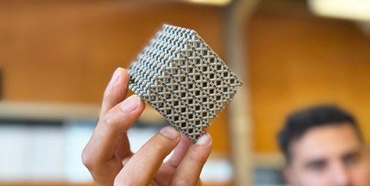
new structure had effectively halved the amount of stress concentrated on the lattice’s infamous weak points. The double lattice design also means any cracks are deflected along the structure, further enhancing the toughness.
Study lead author and RMIT PhD candidate, Jordan Noronha, said that they could make this structure at the scale of several millimetres or several metres in size using different types of AM machines. This manufacturability, along with the strength, biocompatibility, corrosion and heat resistance, makes it a promising candidate for many applications from medical devices, such as bone implants, to aircraft or rocket parts.
“Compared with the strongest available cast magnesium alloy currently used in commercial applications requiring high strength and light weight, our titanium metamaterial with a comparable density was shown to be much stronger or less susceptible to permanent shape change under compressive loading, not to mention more feasible to manufacture,” Noronha stated.
The team plans to further refine the material for maximum efficiency and explore applications in highertemperature environments. While currently resistant to temperatures as high as 350°C, they believe it could be made to withstand temperatures up to 600°C using more heat-resistant titanium alloys, for applications in aerospace or firefighting drones.
“Traditional manufacturing processes are not practical for the fabrication of these intricate metal metamaterials, and not everyone has a laser powder bed fusion machine in their warehouse,” he said. “However, as the technology develops, it will become more accessible and the printing process will become much faster, enabling a larger audience to implement our high-strength multi-topology metamaterials in their components. Importantly, metal 3D printing allows easy net shape fabrication for real applications.”
www.rmit.edu.au
Metal Additive Manufacturing | Spring 2024 110 © 2024 Inovar Communications Ltd Vol. 10 No. 1 | contents | news | events | advertisers | website | newsletter | Industry News
Researchers at RMIT University have developed a new type of metamaterial using a commonly used titanium alloy (Courtesy RMIT)
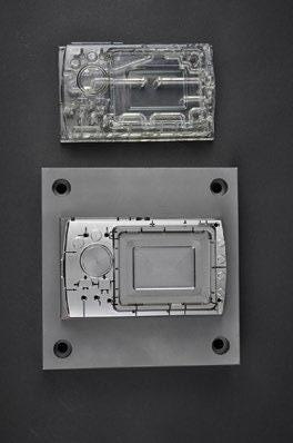
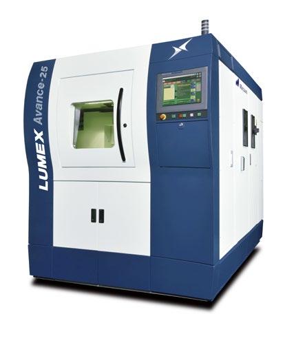


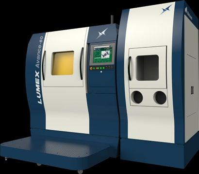
1000 Kelvin integrates AI into EOS Additive Manufacturing software suite
1000 Kelvin, an AI software developer headquartered in Berlin, Germany, has collaborated with EOS GmbH, located in Krailling, Germany, to integrate its co-pilot platform AMAIZE into the EOS software suite. The addition is intended to increase production workflows and enhance the engineering process for customers by harnessing AI.
The integration is expected to enable users to streamline their design processes, reducing engineering costs by up to 80% and accelerating the introduction of new Additive Manufacturing products.
Omar Fergani, CEO of 1000 Kelvin, explained, “The integration with EOS software is a testament to the open architecture of EOS products and the extensive resources of the EOS Developer Network (EDN). These factors have allowed us to seamlessly incorporate the EOSPRINT APIs into our platform, ensuring that our customers can effortlessly benefit from the combined strengths of our technologies.”
Martin Steuer, EOS’s SVP Software Division, stated, “AMAIZE’s AI predictive capabilities enable a paradigm
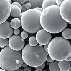
Due to the efficiency of our cuttingedge technology we can offer the lowest priced powder on the market with no compromise in quality. Our powder is:

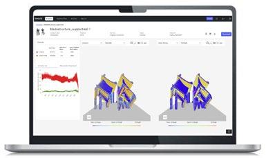
1000 Kelvin will integrate its AI co-pilot platform AMAIZE into the EOS software suite (Courtesy 1000 Kelvin)
shift from physical to digital iteration. This is an important step forward to the industrialisation of Additive Manufacturing. Coupled with its robust cybersecurity, AMAIZE represents a significant advancement in cloud-based solutions for the industry. We’re pleased that EOS customers have now access to this value-added service within our open ecosystem platform and our EOS Developer Network Partner 1000 Kelvin.”
EOS users will be able to access AMAIZE directly by contacting 1000 Kelvin.
www.1000kelvin.com
www.eos.info
Granutools releases GranuFlow software update
Granutools, based in Awans, Belgium, has unveiled new software to pair with the GranuFlow powder and granular material flowmeter for enhanced powder analysis.
The instrument fits the flowing curve to a theoretical model, and from this, it derives two critical indexes that encapsulate the unique interplay of flowability and cohesiveness of the powder. These indexes are then integrated into a comprehensive diagram, providing a holistic view of the powder’s characteristics.
Granutool’s new software takes users through each step via a streamlined interface, enabling precise measurements and reproducible results. The latest update includes the following new features:
A redesigned interface to enhance navigation
• Improved handling of scale calibration validity, enabling measurement accuracy through mandatory calibration
A step-by-step guide to the measurement process, making it easier for operators to obtain reliable results
• Compliance with CFR 21 Part 1, for data integrity and security
• The ability to export data to Excel and PDF
• A display of average values and error bars from repeatability tests
• Automatic connection to the GranuFlow instrument
www.granutools.com
Metal Additive Manufacturing | Spring 2024 112 © 2024 Inovar Communications Ltd Vol. 10 No. 1 | contents | news | events | advertisers | website | newsletter | Industry News RevolutionaRy Results demand RevolutionaRy powdeR POWDER ISO 9001:2015 and AS9100D Certified A division of Arcast Inc. www.arcastmaterials.com
• Free-flowing
D50 of 35µm for most materials
D50 of 20µm for titanium super alloys
Has high tap density
process directly from: Raw elemental material • Pre-alloyed stock
Sponge • Recycled chip
Recycled parts • Over-sized powder • We can handle refractory and reactive alloys •
Spherical
•
•
•
• We
•
•
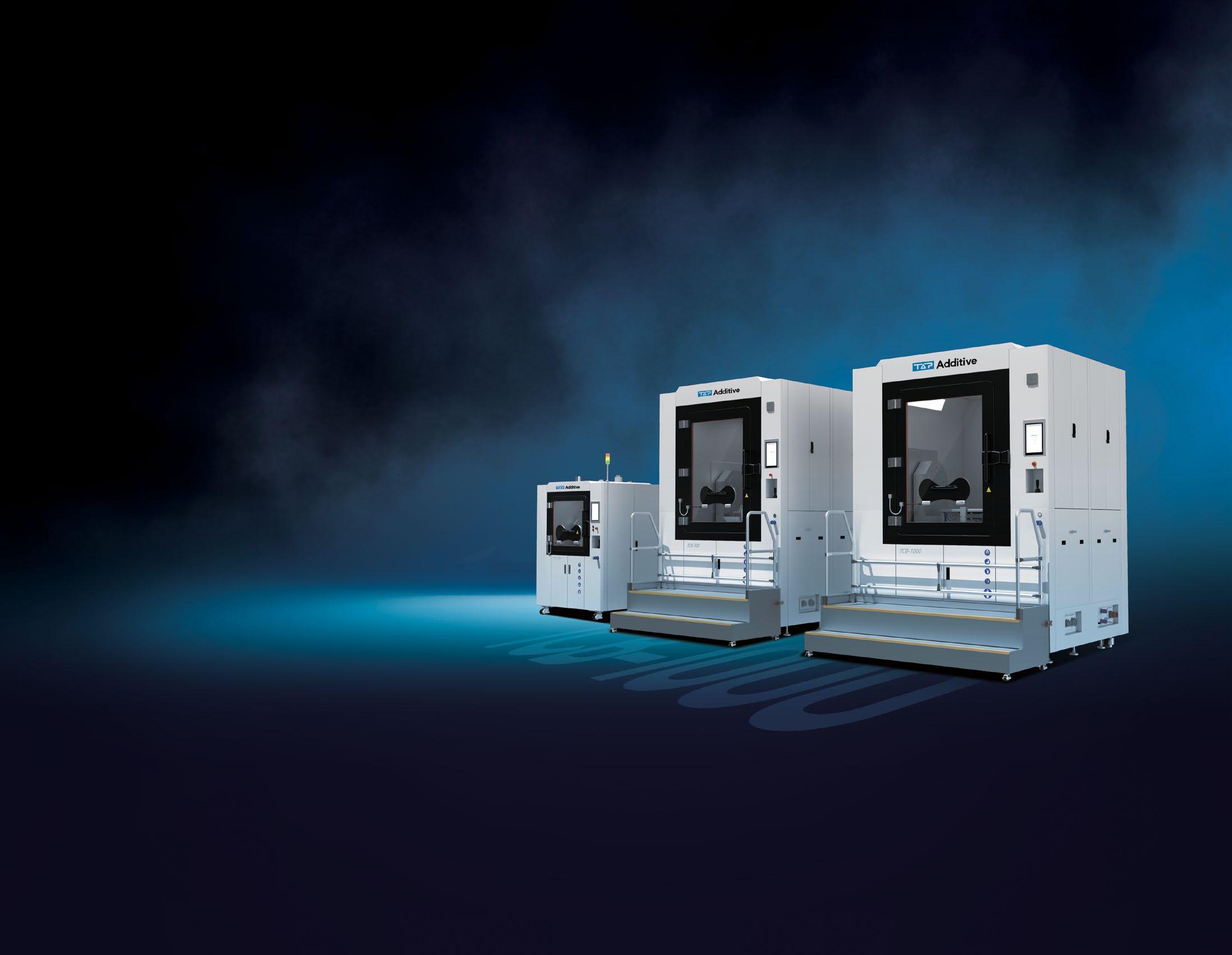
MIT demonstrates rapid Additive Manufacturing with liquid metal
Researchers from the Massachusetts Institute of Technology (MIT), Cambridge, USA, have developed an Additive Manufacturing technique able to rapidly manufacture largescale parts with liquid metal in just minutes. The Liquid Metal Printing (LMP) technique involves depositing molten aluminium along a predefined path into a bed of tiny glass beads. The metal then hardens into a 3D structure. The MIT researchers have stated that this technology is more efficient and at least 10X faster than comparable metal Additive Manufacturing processes.
In a recent study, the researchers demonstrated the procedure by additively manufacturing aluminium frames and parts for tables and chairs which were strong enough to withstand post-processing machining. They showed how components made with LMP could be combined with high-resolution processes and additional materials to create functional furniture.
“This is a completely different direction in how we think about metal manufacturing that has some huge advantages. It has downsides, too.
MIT Researchers have used Liquid Metal Printing to quickly additively manufacture parts such as chair frames and table legs (Courtesy MIT)
But most of our built world — the things around us like tables, chairs, and buildings — doesn’t need extremely high resolution. Speed and scale, and also repeatability and energy consumption, are all important metrics,” stated Skylar Tibbits, associate professor in the Department of Architecture and co-director of the Self-Assembly Lab, who is senior author of a paper introducing LMP.
Tibbits is joined on the paper by lead author Zain Karsan SM ’23, who is now a PhD student at ETH Zurich; as well as Kimball Kaiser SM ’22 and Jared Laucks, a research scientist and lab co-director. The research was presented at the Association for Computer Aided Design in Architecture Conference and recently published in the association’s proceedings.
Drawing on previous work with rubber, the researchers built a machine that melts aluminium, holds the molten metal, and deposits it through a nozzle at high speeds. Large-scale parts can be manufactured in just a few seconds; the molten aluminium cools in several minutes.
“Our process rate is really high, but it is also very difficult to control; it is more or less like opening a faucet. You have a big volume of material to melt, which takes some time, but once you get that to melt, it is just like opening a tap. That enables us to print these geometries very quickly,” Karsan explained.
The team chose aluminium because it is commonly used in construction and can be recycled cheaply and efficiently. Metal coils inside the furnace heat the metal to 700ºC, slightly above aluminium’s 660ºC melting point. The aluminium is held at a high temperature in a graphite crucible, and then molten material is gravity-fed through a ceramic nozzle into a build bed along a preset path. By injecting the molten material directly into a granular substance, the researchers don’t need to use supports to hold the aluminium structure as it takes shape.
They experimented with a number of materials to fill the bed, including graphite powders and salt, before selecting 100-micron glass beads. The tiny glass beads, which can withstand the extremely high temperature of molten aluminium, act as a neutral suspension so the metal can cool quickly.
“The glass beads are so fine that they feel like silk in your hand. The powder is so small that it doesn’t really change the surface characteristics of the printed object,” Tibbits said.
Moving forward, the researchers want to keep developing the machine so that they can enable consistent heating in the nozzle to prevent material from sticking, and also achieve better control over the flow of molten material.
www.mit.edu
Metal Additive Manufacturing | Spring 2024 114 © 2024 Inovar Communications Ltd Vol. 10 No. 1 | contents | news | events | advertisers | website | newsletter | Industry News
Researchers additively manufactured aluminium frames which were strong enough to withstand post-processing machining (Courtesy MIT)

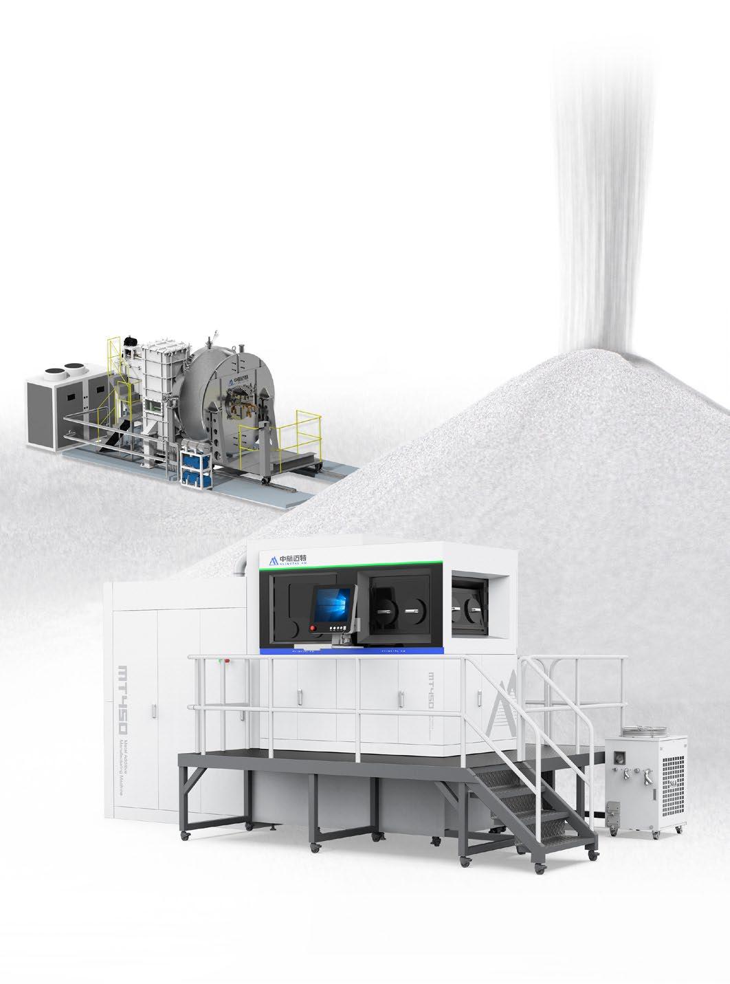



High Performance Metal Powder Advanced Metal 3D Equipment PM Equipment www.avimetalam.com sales@avimetalam.com helen@avimetalam.com +86 138 1025 1750 Sao Paulo,Brazilian Jan,24-27,2024 Booth:C104
Trumpf and Elementum 3D help redesign Intense Cycles’ classic M1 downhill race bike
Elementum 3D, Thornton, Colorado, USA, has partnered with Trumpf, based in Ditzingen, Germany, to additively manufacture major components for Intense Cycles’ M1 downhill race bike. The updated version of Intense Cycles’ classic M1 will feature the bike’s ‘backbone’ bottom bracket and suspension foundation additively manufactured from A6061-RAM2 alloy.
“I work and ‘think’ in aluminium, so AM opens a new world of creative opportunities for me and my team,” stated Jeff Steber, Intense founder and CEO. “We say Intense merges artistry and engineering, and I am no longer limited to metal sheets and tubes. I have the freedom to create almost any shape I want.”
When working to optimise the M1, Steber settled on producing the bike’s backbone from a single piece of 6061 aluminium. The new design incorporates internal ribbing to make
it stronger and lighter, optimising its suspension; but this made it impossible to create using traditional machining techniques.
The first backbone designs were not seen as ideal for Additive Manufacturing, so Trumpf advised Intense engineers on removing low-angle overhangs to improve the build. Trumpf’s updated build processor TruTops Print increased downskin additive manufacturability from 45° to 25° so the backbone was manufactured with much less overhang-supporting material, reducing the chance for errors, material use, and post-processing required.
With Trumpf’s experience additively manufacturing parts from Elementum 3D’s A6061-RAM2 – a weldable 6061 aluminium – the company was selected to carry out the optimisation alongside the Intense production team.
Christian Lengwenat, Trumpf application engineer for metal AM, stated, “Elementum 3D is professional and responds quickly. It’s comforting to work with a reliable, friendly group. Their advanced material properties and surface finish exceeded our expectations, and we plan to use more Elementum 3D powders in our machines.”
From the first test build, Intense reported that it appreciated A6061-RAM2’s weldability, finding it exactly like working with billetmachined 6061, with no porosity or contamination issues. Trumpf noted the predictable processability, which enabled developing a working build parameter in two weeks and required Additive Manufacturing just two DOEs (designs of experiments) to reach the material’s expected relative density value.
Both companies found A6061-RAM2 ideal for this project, particularly given the resultant parts’ surface finish and accuracy. After the backbone was welded to the frame it was reportedly nearly impossible to determine which parts were additively manufactured, machined, or forged.
Steber remarked, “I’m thankful for the great work Trumpf and Elementum 3D provided. Their guidance and expertise played a critical role in successfully producing our new M1. I am happy to report the M1 finished 2nd at the 2023 UCI Cycling World Championships.”
Based on this project and the bike’s performance, Intense intends to ramp up M1 production and has plans to incorporate Additive Manufacturing into future prototyping projects and other production parts.
www.trumpf.com
www.elementum3d.com
www.intensecycles.com

Metal Additive Manufacturing | Spring 2024 116 © 2024 Inovar Communications Ltd Vol. 10 No. 1 | contents | news | events | advertisers | website | newsletter | Industry News
Advertisers’ index & buyer’s guide Looking for AM machines, metal powders or part manufacturing services? Discover suppliers of these and more in our advertisers’ index and buyer’s guide, pages 197- 202
Intense Cycles is updating its classic M1 downhill race bike with an additively manufactured backbone (Courtesy Intense Cycles)
The
Ipsen DS1 Small Size, Big Impact Industrial Strength Compact Footprint The Ipsen DS1 vacuum debinding and sintering furnace offers load dimensions of 12” x 12” x 24” (305 mm x 305 mm x 610 mm). Also available in additional sizes. IpsenGlobal.com/AM
New
Farsoon and Deep Blue Aerospace collaborate on large-scale rocket combustion chamber manufacturing
Farsoon Technologies, based in Changsha, China, has collaborated with Deep Blue Aerospace, Nantong, Jiangsu, China, to additively manufacture a 600 x 780 mm rocket engine combustion chamber that has been developed for commercial launch projects. Together, engineers from Farsoon and Deep Blue Aerospace’s R&D teams addressed key technical aspects, and dedicated months in testing and verification before the completion of the project. The achievements included the successful implementation of machine and process optimisations, targeting high productivity and enhanced quality.
The manufacturing process featured improved items such as the optical system, process parameters, scanning strategy, powder recoating, electrical engineering, and more. After the optimisation, the production time for this combustion chamber was reduced from 327 hours to the current 96.5 hours, representing a significant 338% increase in build efficiency.
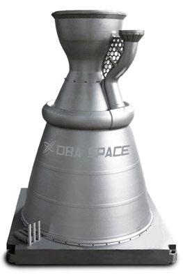
The success of this joint R&D project holds significant importance for Farsoon as it aims to enhance the production efficiency in large-format metal Powder Bed Fusion (PBF) solutions. The key research and application innovations in the project included:
Scanning Strategy
Farsoon implemented advanced multi-laser scanning strategies and a fast-performing algorithm in overlapped areas, addressing challenges in laser power control, galvo system calibration, overlap consistency, and multi-laser task coordination. The enhanced control of the scanner and galvo significantly improved communication efficiency by 39% while ensuring metallurgical quality.
Gas Flow
Gas flow design was optimised for the large-format platform to enable smoke removal and smooth operation of multiple lasers, preventing energy dissipation during the down-wind side laser operation generated by smoke and dust during the build process.
Control System
Farsoon’s R&D team optimised the control system to reduce waiting between the lasers and minimise the downtime of the machine. As a result, the multi-laser platform is able to offer higher efficiency in laser output for significantly improved build efficiency.
Optimised parameters
A smooth surface is crucial to minimise flow resistance in the intricate internal cooling channels within the combustion chamber of the rocket engine. Farsoon customised the processing parameters to achieve the desired high-quality surface that the application requires.
www.farsoon.com
www.dbaspace.com
AML3D receives AS9100D Aerospace Quality Management accreditation for its DED Additive Manufacturing
AML3D Limited, headquartered in Edinburgh, Australia, has received the Aerospace Quality Management System, AS9100D:2016 Accreditation (“AS9100D”) for its WAM technology, a form of wire-based Directed Energy Deposition (DED), which is also known as Wire Arc Additive Manufacturing (WAAM). AML3D is reported to be one of only two DED companies in the world to have the AS9100D accreditation.
The accreditation will enable AML3D to manufacture flight and non-flight components which will be certified for the aviation and defence industries. This provides the company with a significant competitive advantage when bidding for Aerospace and Defence contracts.
“Having the ambition to target and then achieve AS9100D accreditation is a significant milestone for AML3D and is a great credit to the talent, expertise and dedication of our people,” stated Sean Ebert, AML3D’s Chief Executive Officer. “It demonstrates our ability to deliver the highest quality components into the aviation, space and defence sectors; enhances our credibility and reputation as a leading provider of advanced Additive Manufacturing solutions and positions AML3D as a highly competitive player in the Aerospace market.”
“We are continuing to see momentum build in our US ‘Scale-up’ strategy, which delivered over $12 million of orders in 2023, and expanding further into the US and other significant global Aerospace and Defence sectors, a key part of AML3D’s growth strategy, will be helped by having AS9100D,” added Ebert.
aml3d.com
Metal Additive Manufacturing | Spring 2024 118 © 2024 Inovar Communications Ltd Vol. 10 No. 1 | contents | news | events | advertisers | website | newsletter | Industry News
Farsoon has collaborated with Deep Blue Aerospace to develop this combustion chamber (Courtesy Farsoon Technologies)
Mantle reports new customers and highlights users of its toolmaking AM technology
Mantle Inc, San Francisco, California, USA, has reported how its customers are automating their toolmaking with the company’s metal Additive Manufacturing technology. In addition to these user case studies, Mantle announced new customers for its metal Additive Manufacturing machines.
Medical device tooling
Westminster Tool, a comprehensive injection mould builder with a specialisation in class 101 medical device tooling, acquired its first Mantle AM machine in June 2022. Since then, the company has been exploring new applications and testing the flexibility of Mantle’s technology.
With Mantle, Westminster Tool produced steel mould inserts in four weeks. Westminster Tool estimated it would have taken eight weeks with traditional manufacturing to build the same set of inserts, thereby allowing its customers to accelerate their product development process. The additively manufactured tools required minimal finishing and reduced labour & machining time by
Easing labour scarcity
Recognising the growing scarcity of skilled toolmakers, General Pattern, an injection moulder with in-house tooling services and more than 100 years of experience, is addressing the issue by introducing Mantle’s AM machine to automate its toolmaking processes and bolster capacity. General Pattern anticipates that this investment will result in heightened efficiency, decreased reliance on specialised labour, and improved customer service through faster and more efficient operations.
“Introducing Mantle into our operations has elevated our approach to toolmaking. With the simple press of a button, we can now effortlessly create tools, which completely changes our ability to tackle labour challenges and enhances our capacity to better serve our customers,” stated Denny Reiland, CEO at General Pattern. “Recently with a slide for a transportation trim component, for example, we skipped the finishing process entirely. Instead, we printed it, assembled it into the mould, and immediately began moulding parts. This not only saved us the forty hours
Ted Sorom, CEO and co-founder of Mantle, shared, “Mantle’s technology remains a game-changer in the toolmaking industry, consistently driving reductions in lead times and costs while addressing labour shortages. The latest deployments, with Spectrum Plastics Group, Heyco, and General Pattern, coupled with the ongoing success of our existing customer, Westminster Tool, underscore the growing adoption and effectiveness of our technology.”
Customer expansion
Continuing the momentum in the field of medical device manufacturing, Mantle also revealed that Spectrum Plastics Group, a DuPont Business and medical contract manufacturer, will be implementing the company’s metal Additive Manufacturing technology within its facilities.
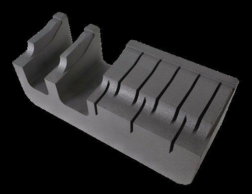
Mantle also announced that Heyco Products, a company under Penn Engineering that specialises in wire protection and termination for various industries, has incorporated Mantle’s metal AM technology into its toolmaking workflows.
“At Heyco, we pride ourselves on taking products from design through to volume production, which includes in-house prototype and production tooling. Mantle allows us to increase our toolmaking capacity and project speed by automating a portion of our toolmaking process, helping to maximise our skilled resources,” stated Danny Anthony, Vice President of Operations at Heyco Products.
www.mantle3d.com
Metal Additive Manufacturing | Spring 2024 120 © 2024 Inovar Communications Ltd Vol. 10 No. 1 | contents | news | events | advertisers | website | newsletter | Industry News
Using Mantle’s metal Additive Manufacturing, General Pattern saved forty hours of active toolmaker time (Courtesy General Pattern)
A Mantle AM machine is shipped from Mantle headquarters to Spectrum Plastics Group (Courtesy Mantle)
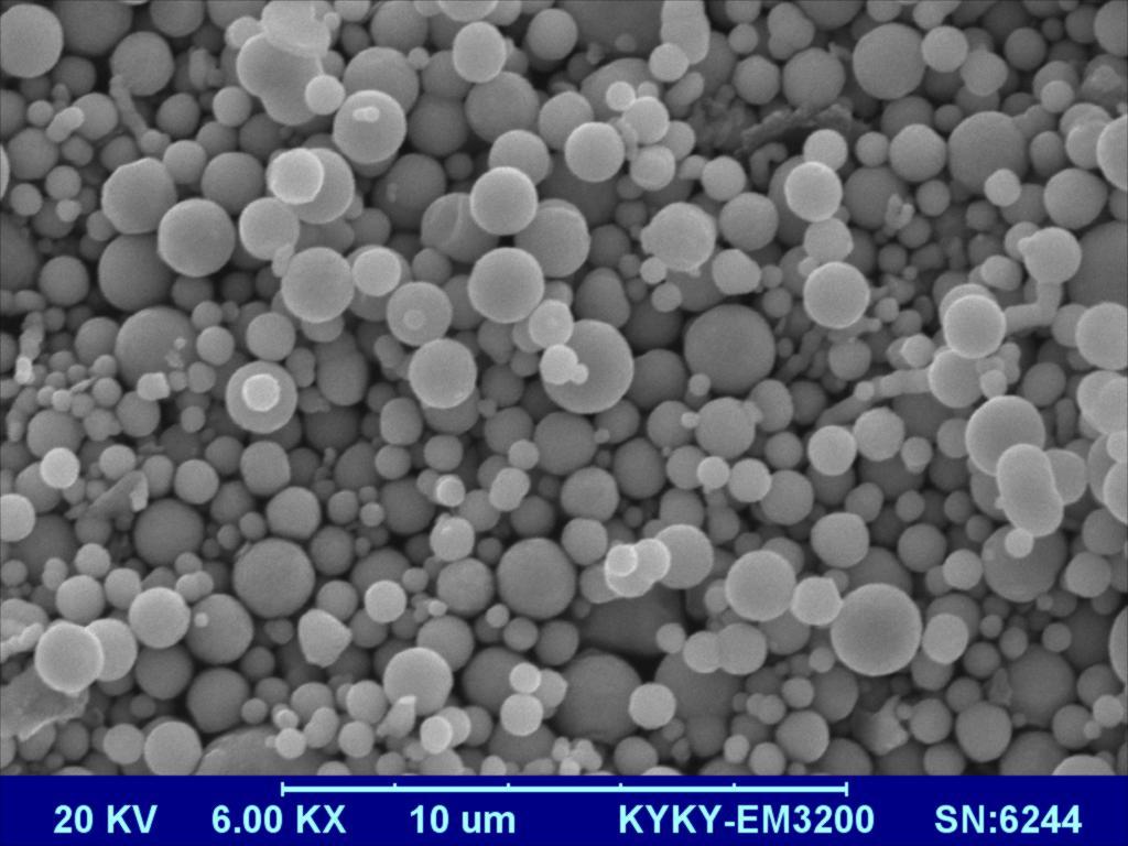
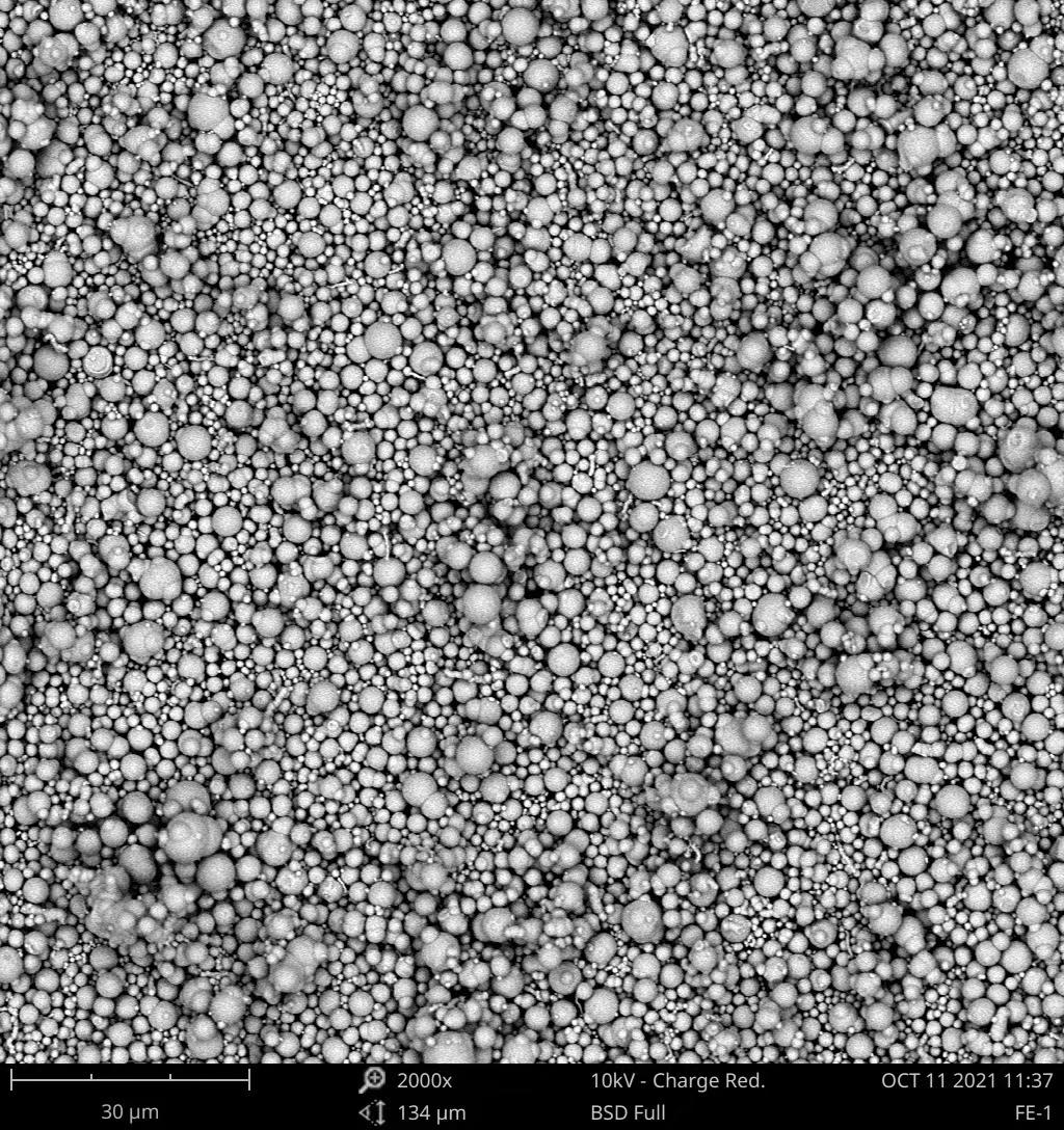
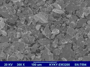
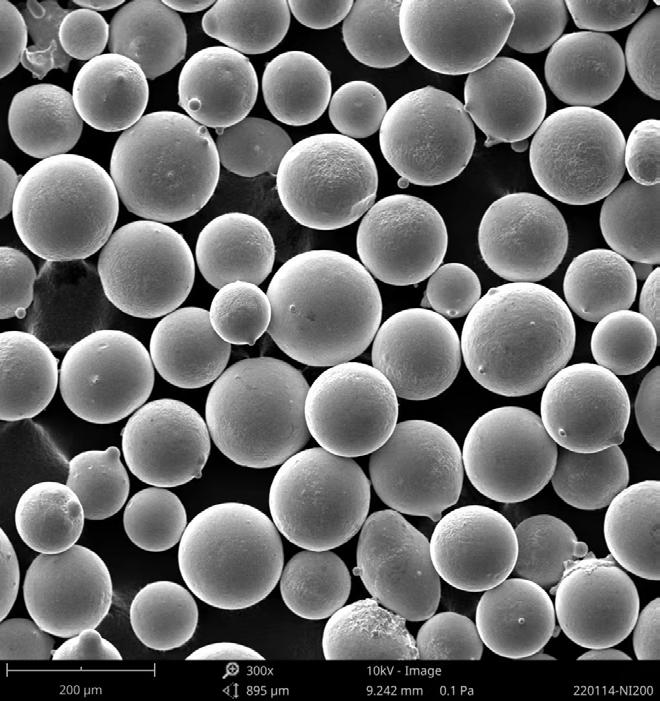
Soft Magnetic Powder Carbonyl Iron Powder Atomized Alloy Powder Microwave Absorbing Material www.yueanmetal.com oversea@yueanmetal.com


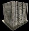
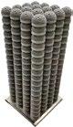
f o r m n e x t
Lincoln Electric and BPMI to support US Navy with large-scale metal Additive Manufacturing
Lincoln Electric, Cleveland, Ohio, USA, has announced that its largescale Additive Manufacturing solution was selected by Bechtel Plant Machinery, Inc. (BPMI) to support the US Navy. As part of the development programme, Lincoln Electric will additively manufacture propulsion components measuring over three metres in diameter and weighing up to 9,000 kg.
“We are proud to continue expanding our network of strategic programme partners to the US Navy,” commented Barbara Staniscia, BPMI President and General Manager. “Metal Additive Manufacturing is pivotal to driving innovation and supply chain resilience, enabling the programme to deliver advanced capabilities to the US Navy.”



Mark Douglass, PhD, Business Development Manager, Lincoln Electric Additive Solutions, shared, “We are pleased to be a strategic partner to BPMI and support the US Navy’s goal to accelerate shipbuilding. We believe our advanced manufacturing process, supported by in-house wire feedstock production and industry-leading application, automation and metallurgical expertise can add significant value in meeting the US Navy’s goals.”
Lincoln Electric reportedly operates the world’s largest wire-based metal AM platform at its facility in Cleveland, Ohio, and is fully vertically integrated with high-volume wire manufacturing across a range of alloys, 3D robotic


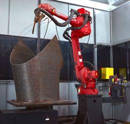
Lincoln Electric’s
by BPMI to support the US Navy (Courtesy Lincoln Electric)
cell integration and proprietary software. The state-of-the-art Additive Manufacturing solution rapidly builds large-scale, metal-based parts directly from CAD files up to eight times faster than traditional casting or forging methods.
additive.lincolnelectric.com
www.bpmionline.com











Metal Additive Manufacturing | Spring 2024 123 Vol. 10 No. 1 © 2024 Inovar Communications Ltd | contents | news | events | advertisers | website | newsletter | GETPDF www.eltra.com ELEMENTAL ANALYSIS OF METAL POWDERS & FEEDSTOCK ELTRA’s new and innovative ELEMENTRAC series is a mile stone for C/S and O/N/H analysis in Powder Metallurgy and Additive Manufacturing: easy to use, fast analysis times and reliable results for metal powders and processed samples. Eltra-Advert-GB-PowderMet-175x120.indd 2 12.02.2024 14:38:48
Industry News
large-scale Additive Manufacturing has been selected
One Off Robotics and Meltio introduce turn-key metal AM cell
Meltio, headquartered in Linares, Spain, has collaborated with One Off Robotics, Chattanooga, Tennessee, USA, to introduce the One Off Robotics Cell, a metal Additive Manufacturing work cell designed for a faster, more efficient, and reliable part production. The One Off Robotics Cell is a robotic metal Additive Manufacturing system powered by Meltio’s wire-based laser Directed
Energy Deposition (DED) process –which the company refers to as Laser Metal Deposition (LMD).
With a deposition rate of up to 1 kg an hour, the machine is intended to manufacture clean, fully dense, and mechanically equivalent or superior parts compared to those created from traditional means. Its 8-axis system simplifies complex geometry manufacturing and is configured to
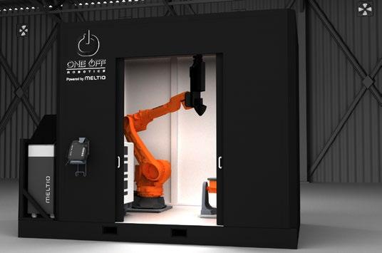
Toolcraft AG extends its AM fleet with Trumpf TruPrint 3000
toolcraft AG, based in Georgensgmünd, Germany, has added a new Trumpf TruPrint 3000 to its fleet of ten Laser Beam Powder Bed Fusion (PBF-LB) Additive Manufacturing machines. The company also announced its Additive Manufacturing with TruPrint machines has been certified in accordance with ISO/ASTM TS 52930:2011 and 52920:2013, according to requirements for industrial AM processes, qualification principles, and production sites. This certification is important for systems that are used in the medical
engineering, aerospace and semiconductor sectors.
The new TruPrint 3000 is a medium-format PBF-LB Additive Manufacturing machine with industrial part and powder management. The TruPrint 3000 incorporates two lasers and has a build volume comprising a diameter of 300 mm and a height of 400 mm.
“Stable processes, reproducibility, service and data security were important criteria for us during the decision-making process. As a long-standing partner, Trumpf has proven itself
work with the Meltio Space robotic slicer, as well as other robotic additive software.
The One Off Robotics Cell uses standard welding wire. The robot and positioner are installed on a selfsupporting platform inside a custom, laser-safe enclosure, which ensures safe operation and quick installation. The system package includes the robot, wire laser metal deposition machine, two-axis positioner, vision laser alignment tool, welding camera, and safety enclosure. Package add-ons are available for the thermal SWIR camera, multi-material dual wire manufacturing, and hot wire manufacturing for increased speed. Meltio and One Off Robotics will also provide system training and instructional materials upon delivery to ensure unparalleled technical support for end users in any industry.
Nick Johnson, CEO of One Off Robotics stated, “One Off Robotics has spent years designing and building large-format robotic additive manufacturing work cells. We’re thrilled to expand our offerings to include a turnkey Meltio Robotic additive system. Our focus is customer success, so we designed this system from the ground up to be quickly installed and easily operated.”
www.meltio3d.com
www.oneoffrobotics.com
time and time again over our many years of working together and totally convinced us on all these points,” stated Stefan Auernhammer, Additive Manufacturing Business Unit Manager at toolcraft.
toolcraft is primarily planning to use its new machine for series production in the semiconductor, aviation and pressure equipment sectors.
“We want to use the integrated melt pool monitoring system to expand our knowledge of the process and we are confident that we can take the quality, reliability and efficiency of the melting process to the next level,” added Auernhammer.
www.toolcraft.de
www.trumpf.com
Metal Additive Manufacturing | Spring 2024 124 © 2024 Inovar Communications Ltd Vol. 10 No. 1 | contents | news | events | advertisers | website | newsletter | Industry News
Meltio and One Off Robotics have collaborated to introduce the One Off Robotics Cell (Courtesy Meltio)
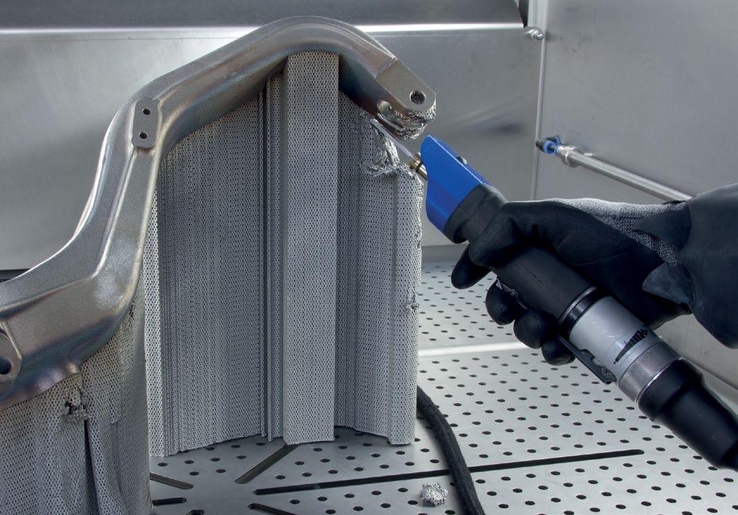
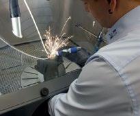
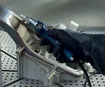

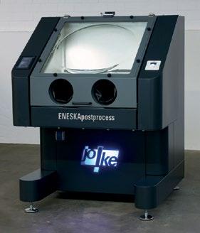
joke Technology GmbH Asselborner Weg 14 -16 51429 Bergisch Gladbach, Germany Phone +49 2204 8390 | Mail info@joke.de www.joke-technology.com The full range of AM postprocessing equipment 100% made in Germany The safe postprocessing system for all materials and work steps ENESKApostprocess Surface Technology

The demands on industrial production are constantly increasing. A rising need for complex and individualized parts, even shorter product cycles, a scrutinization of proven supply chains plus a desire for increased sustainability in this transformation – these are the challenges faced by industries worldwide. It is also a chance for AM to showcase its expertise and creativity. Formnext 2024 provides the ideal platform to showcase your solutions in Additive Manufacturing or along the entire process chain. Actively design the future of production. Register now as an exhibitor at Formnext and request an offer without any obligation. Where ideas take shape. Your answer to the challenges of modern production 19 – 22.11.2024 FRANKFURT / GERMANY formnext.com Honorary sponsor Messe Frankfurt Group
Metal powders in Additive Manufacturing: An exploration of sustainable production, usage and recycling
Sustainability has risen to the top of the global manufacturing agenda. Whilst metal AM has long been considered a green technology because of its net-shape capabilities, it is far from being a process absent of environmental impact. Here, Martin McMahon explores how global efforts are being made to improve this through the use of more sustainable metal powders, combined with a greater focus on powder reuse and recycling. Inextricably linked to this are, of course, economic gains and, in terms of supply chain, national security benefits.
Over the many years that I’ve been involved in metal Additive Manufacturing, one particular area of interest for me has been the environmental impact of producing parts this way; what is now being viewed in the wider context as ‘sustainability.’ Whilst this has become a very significant matter in the last five years, it is a subject that has always been important to AM parts producers, even if they weren’t labelling it as such.
So, how is it that sustainability took hold from the background? Well, reusing powders from the machines that make parts has always been a critical factor for profit; many have always referred to this as ‘recycling’ the powder. Now that green policies and initiatives have risen to the top of policymakers’ agendas, it is loud and clear that sustainability is a label to lean into. After talking to some of the producers and suppliers from across the stock metal powder sector, this article will try to delve deeper into the recycling of materials – including what the term actually means and the reality behind the move towards sustainability.
Scrap underlines sustainability
Many powder suppliers and materials producers are now routinely talking about and publicising their efforts to be more sustainable. At last year’s Euro PM2023 conference’s plenary
session, I heard something that really struck a chord with me. Teemu Karhumaa, Head of Research And Development at Tikomet Oy, stated, “scrap is the new gold." He also noted how the near future will bring huge competition for secondary raw materials as the world seeks to reduce
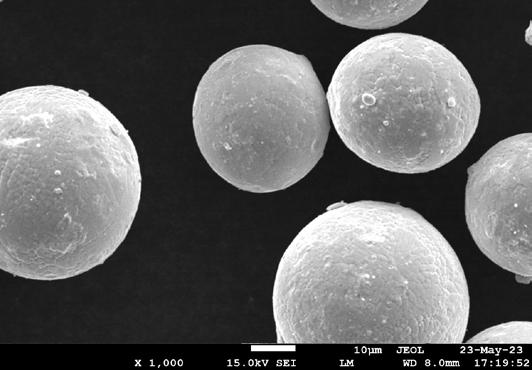
Metal Additive Manufacturing | Spring 2024 127 Vol. 10 No. 1 © 2024 Inovar Communications Ltd | contents | news | events | advertisers | website | newsletter | GETPDF Sustainability and metal powders for AM
Fig. 1 This nickel superalloy, OptiPowder 718, from Continuum Powders, is the first alloy qualified for Velo3D's Sapphire machine to be produced from a 100% recycled feedstock (Courtesy Continuum)
in automotive electrification and a net-zero emissions company by 2037 throughout the whole value chain (Courtesy Höganäs AB)
costs for the production of metallic materials and the environmental impact of producing them. To me, this really did underline the potential value of recycling materials for the production of metal powders.
Sustainability in the materials supply chain is probably what has always driven the scrap metals industry. Anyone working in the production of steel or aluminium alloys would not consider this a new concept and could tell you that scrap metal is a key feedstock material. Perhaps not so recognised, though, is that recycled materials are also already used in bulk for
the production of common metal powders. It is hard to imagine any powder producer with annual outputs in the thousands of tonnes of steel, for instance, that doesn’t already rely on scrap in order to keep costs down. They have perhaps just been a little shy to publicise this fact before now. This makes perfect sense, however, considering the abundance of scrap stainless steel in the world (the same is very likely for nickel-based alloys, aluminium, and also copper, though this is probably not so for reactive metals).
Before sustainability became a mainstream area of focus for all
industries and governments, the output of parts across the spectrum of Powder Metallurgy, including Metal Injection Moulding (MIM), press and sinter, and Hot Isostatic Pressing (HIP) has included powder incorporating recycled materials. In this respect, the circular economy is also nothing new.
In the early years of metal AM, however, those producing powder specifically for the industry – and therefore generally in smaller quantities – were likely to be doing so from either pre-alloyed billets or by introducing elementals directly into the crucible. Now, with the greater realisation that it is everyone in industry’s responsibility to care for the environment, we can see a drive to set concrete targets to create a cleaner, more sustainable supply chain for metal powders to be used in AM. If nothing else, with a wider spectrum of end-users and consumers who are making demands for it, it’s likely to be a differentiator in many purchasing decisions.
We saw this last year during Formnext when a few mainstream suppliers – including Tekna and Höganäs – had part of their exhibition displays focused on recycling and sustainability. The AM machine supplier, EOS, also said it will be pursuing changes to its powder specifications this year, starting with AlSi10Mg. The company now requires its suppliers to include at least 30% recycled materials in any feedstock, claiming that this will result in a 25% reduction in CO 2 emissions.
Some of the newer powder and powder manufacturing technology suppliers that have made sustainability a central part of their business from ‘go’ were also at Formnext. Companies such as Amazemet, coming out of Poland with its ultrasonic rePOWDER atomisation technology; 6K Additive Inc, from the USA, focusing on making powders from recycled materials with the proprietary UniMelt® microwave plasma system; and Continuum, also from the USA, which has introduced its Greyhound M2P system for producing powder using 100% recy -
Metal Additive Manufacturing | Spring 2024 128 © 2024 Inovar Communications Ltd Vol. 10 No. 1 | contents | news | events | advertisers | website | newsletter | Sustainability and metal powders for AM
Fig. 2 Höganäs AB, the world leader for iron powder production, has an annual production capacity of 500,000 tons, as well as offering advanced powders for AM. The company is transforming itself to become a key player
cled feedstock materials (Fig. 1).
Metal Additive Manufacturing has a great opportunity to take a global lead in sustainable manufacturing. It has the potential to use far less material and energy, and make less of an impact on the environment than those processes that have come to be considered ‘conventional’ methods. But where in the end-toend process chain do metal powder producers make their contribution to sustainability?
The current state of Additive Manufacturing
When AM first started to become popular a little more than a decade ago, it was introduced as a greener way to produce parts. There was a lot of hype around the fact that AM only used the amount of materials that are in a finished product – it wasn’t unheard of to hear claims that there was almost zero waste in AM. With time, however, comes enlightenment, and we now know for certain that this is not the case; there are inherent levels of wastage dependent on the selected AM process. For example, those working with Laser Beam Powder Bed Fusion (PBF-LB) AM machines should be able to give conservative estimates for the loss of powder per build at between 5-15% of the dispensed powder.
The use of metal powders in Additive Manufacturing is undoubtedly going to continue to grow. This is not only true for the alloys that are already commonly in use, but will include an ever-increasing list of other alloys, driven by two major changes in the machines that use metal powders. First, and rather obviously, there is the size of the machines to consider. As they become larger and feature increasing capacity for producing parts, they will need more powder to fill them. Secondly, there is the diversification of the machines. Where once Powder Bed Fusion was dominant, especially PBF-LB, now there is a growing market for
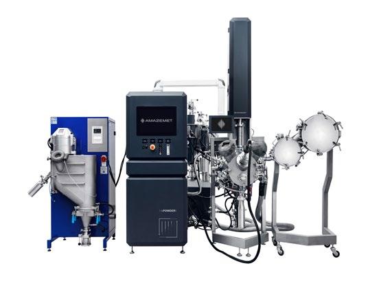
“There was a lot of hype around the fact that AM only used the amount of materials that are in a finished product – it wasn’t unheard of to hear claims that there was almost zero waste in AM. With time, however, comes enlightenment, and we now know for certain that this is not the case.”
Electron Beam Powder Bed Fusion (PBF-EB), Directed Energy Deposition (DED), Binder Jetting (BJT), Material Extrusion (MEX), and Cold Spray (CSAM).
All of these are growing in popularity and require grades of metal powders that are similar or overlap in terms of particle size distribution. All are also competing with other conventional Powder Metallurgy applications, which are also expected to see greater powder requirements.
Powder usage efficiency by AM process type
It follows that as the adoption of each AM process increases, so too will the waste stream of those powders. In terms of sustainability, each metal AM process is capable of recycling feedstock, but this does not always include that portion of powder that is considered ‘waste’. This can be powder that has been lost to filtration systems, entrapped in the mechanics of an AM machine, or
Metal Additive Manufacturing | Spring 2024 129 Vol. 10 No. 1 © 2024 Inovar Communications Ltd | contents | news | events | advertisers | website | newsletter | GETPDF Sustainability and metal powders for AM
Fig. 3 AMAZEMET’s rePowder atomiser offers the low-cost, eco-friendly recycling and ultrasonic atomisation of metal materials at the laboratory scale (Courtesy AMAZEMET)
powder contained in closed volumes of parts or their support structures. In the case of the latter two, there has been a great deal of effort placed on recovering this powder for re-use.
Material Extrusion
Of all Additive Manufacturing processes, it is probably MEX that is the most intrinsically sustainable. Here, fine metal powders are blended with a binder to produce filaments, rods, or pellets for the process, so the process doesn't use dry, loose powder. Since there are no process losses from things like spatter, trapped powder, over-dosing, condensates, or powders carried off into filters or other machine deadspots, there are extremely low levels of wastage. With this technology, one comes closest to using only the materials that are required to build the part, and – more often than not – any unsintered materials can be used directly in the production of new feedstock.
Binder Jetting
Next in the line of sustainability is Binder Jetting. Even though this is technically a powder bed technology, it involves no in-process melting, and levels of powder recovery from the builds should be very high. There can be small losses from trapped volumes of powder, and there is a risk of contamination from stray jets of binder into the powder bed, but, compared to fusion-based processes, the recyclability of used powder should be intrinsically higher.
Powder Bed Fusion
PBF processes are a little more complex since they do suffer from more losses than the above. In the melting process there are risks that powder is lost as spatter particles or other ejected matter such as fumes, condensate, and fines. The latter two types of particles can sometimes be very heavily oxidised and, for this reason, are not normally considered for re-use or recycling. A question remains over what becomes of this waste stream; in all likelihood, it has ended up in landfill or been incinerated. The so-called ‘recycling of powder’ (which should really be referred to as the re-use of powder in the context of using powder to make parts) in Powder Bed Fusion machines has long been a concern and must be more tightly controlled than in other AM processes.
Some end users have imposed a complete ban on the use of powders that have been previously exposed to any part of the AM process; this is, of course, completely at odds with AM being a sustainable, more environmentally friendly set of processes. If this ethos were to continue, there would be a very uncertain future for these AM processes. However, it is easy to understand the concerns since the early adopters in the industry were themselves in doubt of the true risks of re-using exposed metal powder. This may have been due to a lack of understanding of the processes themselves, the effects of atmospheric exposure on the powders, degradation of composition
“Some end users have imposed a complete ban on the use of powders that have been previously exposed to any part of the AM process; this is, of course, completely at odds with AM being a sustainable, more environmentally friendly set of processes.”
or increased oxidation coupled with inadequate means of assessing used powders, or even a simple distrust of a new, unqualified process. Thankfully, this hasn’t deterred everyone. Other early adopters, including service providers, were very quick to realise the issue and developed their own methods to track the usage and quality of process powders.
Notable successes in metal AM have taken place in the Formula 1, space and medical sectors as a result. Nowadays, industry standards (e.g. AMS 7031 from SAE International) have been published that set out the requirements for the re-use of powder, particularly in PBF machines. This particular standard makes a clear distinction between powders that are simply ‘turned over’ in the machine and used multiple times, and those that are removed from the process, reconditioned to be like new and then re-introduced into the process.
The SAE AMS AM metal committee is also working on another document to address recommendations for machines with closed-loop powder feed systems. It is very clear that the sustainability of powders is now a key factor for any PBF process.
Cold Spray and DED
Closing on the PBF AM processes in terms of popularity are the two deposition technologies, Cold Spray and DED. In CSAM, there is no fusion. Instead, the process relies on extremely high impact energies to co-bond metal particles. While it is possible to use very small amounts of powder for this process, it does suffer from a certain amount of ejected powder, which is not currently considered re-useable and must be discarded after the process.
Conversely, in DED machines, the powders being introduced are completely melted, and there can be large areas of spatter and other melt-related ejected particles, none of which can be re-used in the process. In both types of AM processes, there is a high likelihood that the ejected particles would be heavily oxidised, irrespective of the
Metal Additive Manufacturing | Spring 2024 130 © 2024 Inovar Communications Ltd Vol. 10 No. 1 | contents | news | events | advertisers | website | newsletter |
and metal powders for AM
Sustainability
type of gas used to spray or protect the process, and, quantities permitting, the best that could probably be expected would be for them to be collected and sent back as tertiary ‘scrap.’
Sustainability and metal powder production
Perhaps the most obvious point to make about the current production of metal powders from regular alloy feedstocks is the significant energy consumption and the associated carbon footprint generated by the global logistics of transporting, melting, and forming into the billets, bars, coils, and wire feedstock. This isn’t even considering the initial refinement of ores into elemental metals; this, of course, accounts for very high levels of energy consumption and natural resources.
Whilst AM is said to be greener than conventional processes because one only needs to use a certain
amount of materials contained in each specific part, the powder does have to be produced following these primary methods. When considering AM’s sustainability, we cannot forget to take into consideration the additional energy that is required to melt the feedstock, atomise it, collect and classify the powder, store it safely, and then distribute it for use.
Where does your metal come from?
In the early, most-hyped days of Additive Manufacturing, no one was talking about the yields in the powder production process that made these optimal powders. In many cases, the yield from the atomising process for good powder suitable for Powder Bed Fusion was at best 45% and was frequently as low as 30%. Some powder producers were able to boost the yield up to 60% or even 70% if the different cuts of powder could be used in other forms of AM, such as DED. Nonetheless, in most cases the yields were low and that meant quite a lot of waste product coming out of
the atomising process. Whilst this is still far less than the high percentage of waste generated from fully machined parts, swarf is routinely collected and sent for recycling. However, can the excess powder from atomisation also be recycled?
If we first consider what was thought to be happening in the early years of metal AM, there was a general belief that all powders were being made from primary metal stocks. This would mean that there would be an accumulated environmental impact, starting from the holes in the ground all the way through to atomised powders, significantly higher than other, more conventional manufacturing routes. This belief about metal powder origin was probably a consequence of the many questions about the traceability of those metal powders and how that would affect final part quality. This concern was mainly coming from those buying into AM for future medical and aerospace applications. When anyone was asked
Metal Additive Manufacturing | Spring 2024 131 Vol. 10 No. 1 © 2024 Inovar Communications Ltd | contents | news | events | advertisers | website | newsletter | GETPDF
Sustainability and metal powders for AM
Fig. 4 Trucks and machinery at Chuquicamata, the world's biggest open pit copper mine, Calama, Chile. (Vit Baisa/ Adobe Stock)
“the truth is that if metal powder was always to be produced from virgin raw materials, following the rock-to-billetto-powder process route, then there would be a very significant cost to pay. Worst of all [...] the environmental impact would only become more severe.”
about the traceability of their metals, their response was always that they could provide full traceability back to the hole in the ground. Hence, for most end users, it was natural to assume all powders were made from primary feedstock.
The possibility of using already qualified end-of-life products, off cuts, and revert was hardly ever considered, much less talked about. This was certainly the case for Ti-6Al-4V, which gained popularity in metal AM very quickly. However, the truth is that if metal powder was always to be produced from virgin raw materials, following the rock-tobillet-to-powder process route, then there would be a very significant cost to pay. Worst of all, it would mean that if the use of metal powders continued to grow as currently predicted, the environmental impact would only become more severe.
Improved but imperfect
Where the industry is today, the overall environmental impact of metal powders used in AM still results in increased emissions and an increased carbon footprint. We still have to take into account the extra transportation's energy requirements, and the packaging requirements for metal powders – particularly since much of the powder used today starts its life on the opposite side of the planet to where it is eventually used. Furthermore, metal bar and billets are happy to stay on a shelf,
or in a yard on a pallet, almost indefinitely, whereas metal powders instead have to be kept clean and dry. This involves the use of a lot of plastics – worse still is that these are effectively single-use plastics.
A problem that very few to date have tried to address is just how these containers can be collected and safely recycled. With each container contaminated with metal particles and no known history of exposure, there are no powder producers currently willing to entertain the idea of taking them back, cleaning them and then reusing them. Using containers made from steel or other metals is a little better, but they still use plastic liners and silica gel pouches. This is just one negative environmental aspect that the AM sector is going to have to live with until an alternative solution can be found.
The promise of recycled metals
Far from being the case that all powders are made from virgin primary metal stocks, the situation has changed steadily over the last decade; it is known and accepted that some metal powders do come from recycled secondary feedstock. The main issue now is making sure that the form of scrap is of a suitable size and shape that can be readily melted in a crucible.
The AM sector has also started to see new suppliers concentrating on sourcing from this part of the supply chain, with some even introducing new technologies with the sole intention of being more sustainable. A great deal of interest from the academic world has also led to more research initiatives, such as the recently published work by University College London involving recycled steel via the electric arc furnace (EAF) route. In that paper, it was estimated that EAF saw a significant reduction in greenhouse gas emissions of 86%; energy consumption of 85%; water pollution of 76%; and water usage of 40% compared to primary extraction and the blast furnace route [1].
In terms of CO 2 emissions, the Fraunhofer Institute for Material and Beam Technology (IMWS) found that using one tonne of recycled stainless steel scrap could save approximately 4.3 tonnes of CO 2 when producing steel [2]. This is all very good if scrap is then used as the feedstock for making powders – and companies, such as Mimete, have been involved in a complex pan-European project, which includes universities and research institutes, to estimate the effect of different feedstocks on the carbon footprint of the final powder product.
So, is recycling the simple answer to all environmental problems? A succinct answer to this came from Bruce Bradshaw at 6K Additive, one of a new generation of greener powder producers, “For AM applications, you can use 100% recycled material, but not all recycled material can be used for AM applications.”
What makes scrap?
This makes the scrap-to-powders route an interesting topic. It avoids the time-consuming, expensive, and carbon-intensive primary feedstock processes, but does come at the cost of losing easy control of the chemistry. This then places a very high level of importance on the selection of specific grades of scrap for use as a feedstock for making powders. Other companies, such as Pometon,
Metal Additive Manufacturing | Spring 2024 132 © 2024 Inovar Communications Ltd Vol. 10 No. 1 | contents | news | events | advertisers | website | newsletter |
Sustainability and metal powders for AM
added to this by specifying that large pieces of scrap with uniform specific surfaces are preferred, as opposed to turnings or milling chips that can be heavily oxidised and contaminated by coolant oils.
One of the first things to consider is the definition of ‘recycled materials,’ which, to most, will include both scrap and waste. Scrap can come from end-of-life products that are re-processed, chopped up into pieces and then remelted. However, this requires the correct controls to segregate the types of alloys, including the grades and perhaps the certified origins. Scrap can come from materials that remain at the end of the primary production process that, in theory, have not been exposed to any other changes. This is already a very common form of scrap, known as revert, used in the casting industry.
Waste, however, is collected downstream from manufacturing or fabrication processes and can include off-cuts, trimmings and swarf. This waste material is usually considered lower quality, being contaminated with oils and chemicals. Dealing with this waste for recycling can be quite energyintensive since it is usually more difficult to segregate, grade, clean and certify in terms of composition.
Stainless steels
Stainless steels are already sorted and segregated into grades that can be fed directly into furnaces to produce like-for-like steels. This happens across all metal – and metal powders – producers. It makes perfect sense because there’s so much of it available and the values of these metals lend themselves to the process. In fact, a recycling supply chain has been in existence for a long time and is already so effective and efficient that it’s hard to imagine any stainless steels currently being used in AM that do not contain very high percentages of recycled material.
Even so, great care and strict quality controls need to be in place to ensure that type compositions are
“
... a recycling supply chain has been in existence for a long time and is already so effective and efficient that it’s hard to imagine any stainless steels currently being used in AM that do not contain very high percentages of recycled material.”
respected. This becomes even more important when satisfying the brand specifications of individual end users.
In cases like this, some contributors stated that they would only ever use a maximum of 50% of scrap, mixing it with virgin elemental material to restore the specific composition of the alloy. In fairness, and with all things being considered, the emis -
sions and carbon footprint associated with the production of stainless steel powders are probably already as low as they can currently be.
In some cases, the calculated reduction in CO 2 and energy consumption is as much as a factor of 10; Sandvik presented data at PowderMet 2023 showing reductions of at least 50% for all feedstock mate -
Metal Additive Manufacturing | Spring 2024 133 Vol. 10 No. 1 © 2024 Inovar Communications Ltd | contents | news | events | advertisers | website | newsletter | GETPDF
Fig. 5 A very high level of importance is placed on the selection of specific grades of scrap for use as a feedstock for making powders, avoiding materials contaminated with oils and chemicals (Dimas/Adobe Stock)
Sustainability and metal powders for AM
Recycled materials [>50% reduction]
“Adding a bit of extra shine to this are companies such as Indo-MIM, Sandvik, and Continuum, which are also relying on renewable energy for their atomising processes. In fact, more and more companies are now seeking to contract with ‘green electricity’...”
rials with respect to virgin materials production (Table 1). It is something that all major global producers of steel have become aware of – a few have even announced their entry to the AM supply chain, including ArcelorMittal in Spain [3] and Outokumpu in Germany (Fig. 6) [4]. The latter describes its whole plant as ‘a large recycling unit’ because taking scrap from its other steel production operations located in the same city. These examples are, at least, gold stars for metal AM.
Adding a bit of extra shine to this are companies such as Indo-MIM, Sandvik, and Continuum, which are also relying on renewable energy
for their atomising processes. In fact, more and more companies are now seeking to contract with ‘green electricity’, which will only be a good thing for the environment. Some companies are willing to go even further with recycling steel, with f3nice in Italy committed to using 100% recycled steel.
Other alloys
Aluminium, titanium, nickel and copper all require vast amounts of energy and natural resources to produce from new. Thankfully, in primary alloy production, there is already a lot of recycled scrap that is used as feedstock, and this is
accompanied by careful control of possible contaminants that could be detrimental to the alloy. So, what’s to stop the same processes from being followed by powder producers?
Up to now, the reason for not doing so could have simply been a matter of economics. Of the suppliers that have contributed to this article, all said that there is a good chance for recycled feedstock of less complex alloys. However, it is recognised that the in-demand alloys are those that are highly engineered, which makes the use of generic scrap quite problematic. Only if the powder production batches are very large will it be possible to achieve safe levels of dilution, so-called ‘alloying up’. For instance, there are many concerns about the use of aluminium scrap – particularly if AM parts are to be used in aerospace applications – and strict controls of levels of beryllium are in place for this reason. Circle Metal Powders in Taiwan was the only contributor to state that it uses secondary aluminium alloys to produce powder under the scope of AS9100-certified procedures.
From a CO 2 perspective, using scrap should be a no-brainer. It was mentioned previously for steels
Metal Additive Manufacturing | Spring 2024 134 © 2024 Inovar Communications Ltd Vol. 10 No. 1 | contents | news | events | advertisers | website | newsletter |
Manufacturing,
materials Emission factor (t CO 2/t) Energy factor (kWh/kg) Cobalt 8.30 35.56 Iron/Steel 2.26 3.65 Chromium 2.40 11.17 Manganese 1.00 6.58 Nickel 11.40 30.83 Copper 2.80 14.92 Molybdenum 5.70 32.50 316L 5.13 Alloy 718 9.63
Table 1 Data from the presentation 'Sustainability of inert gas atomised powders' by Paul A Davies, Sandvik Additive
PowderMet 2023
Virgin
Emission factor (t CO 2/t) Energy factor (kWh/kg) Cobalt 4.15 17.78 Iron/Steel 0.36 0.61 Chromium 1.20 5.58 Manganese 0.50 3.29 Nickel 0.22 15.42 Copper 1.40 7.46 Molybdenum 2.85 16.25 316L 0.62 Alloy 718 0.91
and metal powders for AM
Sustainability
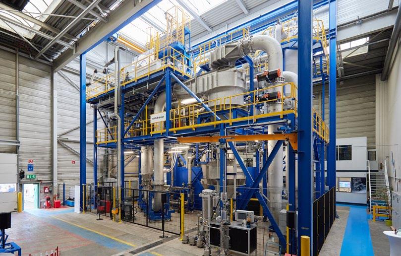
that there are huge differences in the amounts of energy required to produce alloys from ore compared to those same alloys derived from scrap. However, the cost associated with doing the sorting and quality checks could easily balance the savings achieved from using less energy. This would leave only the environmental benefit of lower CO 2 emissions. For some, this could push the all-inclusive use of recycled materials as feedstock for these highly alloyed powders out of the reach of the AM sector for now.
This can be circumvented by the use of recycled feedstock, which comes only as revert, including the off-size, unwanted powders from previous melts. This is something that is already being achieved by companies that are also primary alloy producers, such as Carpenter and Sandvik, since powder revert can be mixed with other revert from the production of the primary alloys.
The economics of powder sustainability
The economics associated with the use of sustainably produced metal powders should be rather straightforward to understand. Each of the powder producers contributing to this article stated that taking revert, primary metal scrap and end-of-life metal parts would not be a new practice and could be useful sources for their own feedstock. The cost reduction in using qualified scrap compared to virgin raw materials is unquestionably significant, coming from vastly lower energy consumption. This, in turn, means that several kilograms of CO 2 per kg of alloy are removed by using scrap feedstock in place of virgin raw materials.
Similarly, most suppliers agreed that the materials that have already been targeted are commodity alloys like stainless steels. 316L is the most popular in AM, used to build parts for general industrial use with
requirements that are not as high as in tightly regulated sectors such as medical and aerospace. To make economic sense the volumes need to be high, but this hasn’t been a significant barrier for them where nickel, copper, and aluminium alloys are concerned since all are very widely used across the industry.
Unfortunately, the cost of assuring quality does still add up in the collection, grading, chemical analysis, cleaning and subsequent stocking of these potential feedstock materials. Hence, the route to produce powder from scrap can still involve a lengthy and somewhat energy-intensive set of processes. Where energy is a factor, cost is very important, particularly when considering the amount of transportation that is required.
These costs are further pushed up by the availability of good quality scrap from assured sources; some have suggested that these accumulated costs could easily match those of the equivalent virgin raw
Metal Additive Manufacturing | Spring 2024 135 Vol. 10 No. 1 © 2024 Inovar Communications Ltd | contents | news | events | advertisers | website | newsletter | GETPDF
Sustainability and metal powders for AM
Fig. 6 Outokumpu, describes its whole atomisation facility as ‘a large recycling unit’ because it is taking scrap from its other steel production operations located in the same city (Courtesy Outokumpu)
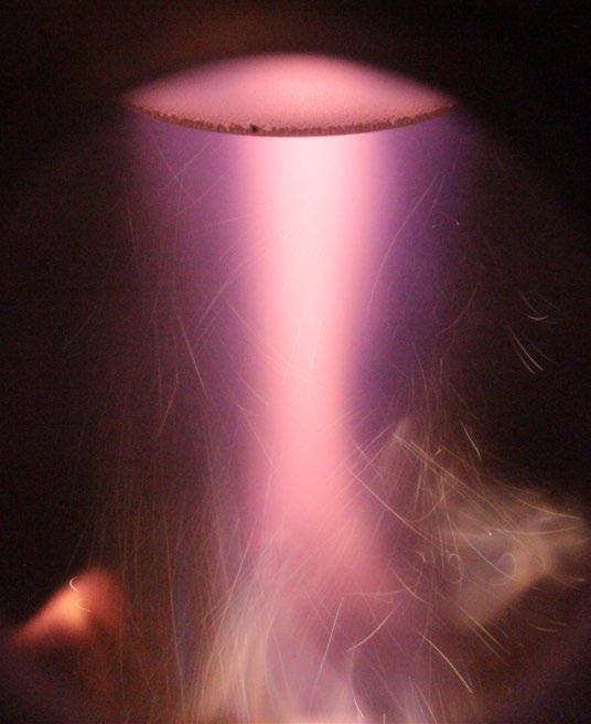
materials. Estimates have been given by those contributing to this article that put savings anywhere between 0% for highly alloyed metals to a conservative maximum of 40% for common grades of stainless steel. This takes into account the full endto-end process chain to produce new powder from scrap. Process savings have been found, with some stating that using scrap does still end up requiring less energy to melt in the furnace.
Another side to this coin is the ‘Green Credit’ that can be earned from using scrap and reducing energy consumption. Several different models and calculations are being used to quantify and apply these credits – some even having
real financial benefits. From a public perspective, this enables the companies to work towards any environmental goals, such as achieving net-zero emissions by 2050.
How have the costs been reduced?
In the earlier days of metal Additive Manufacturing, prices for metal powders were at eye-wateringly high levels for consumers, even for standard alloys like stainless steel, with reactive materials such as Ti-6Al-4V powder being sold at close to $500/kg. Nowadays, the price is closer to $100/kg, especially for larger quantities, but that reduction has come about due to the increased number of suppliers, i.e. greater availability, not higher levels of
recycling. It’s only very recently that 6K Additive, a relatively new supplier to the AM sector, announced a certified route to producing this alloy from scrap, which relies on very tight controls of the environment in the process (Fig. 7). However, they are not alone in tackling this opportunity, with other new suppliers are also targeting the recycling of titanium alloys, including IperionX (Fig. 8) and the Eramet-led EcoTitanium project [5].
In the long run, the economics of using scrap materials for producing powder might not stack up in favour of the AM sector. This is because the whole world is now looking to be more sustainable and is trying to work towards net-zero emissions. So, whilst there are obvious gains to be had in terms of lower energy usage, which will drive costs down, the demand for scrap from across the entire industrial world could eventually drive costs up and keep them there. The growing interest also has the potential to make sourcing high-quality graded scrap more and more difficult.
Recycled or re-used metal powders
Sustainability in the use of metal powders is not just concerned with using secondary sourced feedstock materials for the production of the powder; it also has to include the recycling and re-use of powders that have been through the AM process. It is only when we consider this aspect of sustainability that we can truly understand how powder recycling becomes a direct contributor to the circular economy. It turns out, however, that this is not as straightforward as some may believe and it presents some very complex issues that need to be understood.
Firstly, the different sources of powder that can be recycled, meaning that the powder coming from these sources can be in different conditions. These include revert powder from the atomising process; used powder that has been exposed to
Metal Additive Manufacturing | Spring 2024 136 © 2024 Inovar Communications Ltd Vol. 10 No. 1 | contents | news | events | advertisers | website | newsletter |
Sustainability
metal powders for AM
Fig. 7 6K Additive is focused on making powders from recycled materials with its proprietary UniMelt® microwave plasma system, offering a certified route for making Ti-6Al-4V powder from scrap (Courtesy 6K Additive)
and
one of the metal AM processes; and unused powders, perhaps bought speculatively; in addition, storage can be problematic
Secondly, there are the economics of taking any of this powder back from the market to consider; up to now, it has been managed and paid for by end users. This incremental cost can be a bitter pill to swallow for most.
Revert powders
For revert powder, the main issue for producers is guaranteeing that this powder has not become contaminated. This is not a given, because it may be the case that these waste products are not being stored in sealed containers or a protective environment. However, for steels – and, to some extent, nickel- and cobalt-based alloys, it may still be possible to clean out contaminants during the melting stage and before atomisation. Unfortunately, this is not always the case, and producers of aluminium powders struggle to cleanly remelt compacted oversized particles and fines from their processes because of the oxide layers formed on the powder particles. This could be why none of the contributors to this article have said that they use revert powder.
Used and unused powders
When most people discuss recycled powder, they are actually referring to powder that has been used in an AM process and then returned to that same process. This is a difficult subject, however, since there are differences in opinion on what constitutes ‘used’ powder. This ranges from those who say even the powder in a newly opened container should be then considered ‘used’ to those who say it is what comes out of an AM machine after a build, even extending to multiple cycles and continued re-use or recirculation.
In the best-case scenario, when using powders discarded from a machine, users will have devised their own method for determining when the powder has fallen out of specification. In the worst case, the
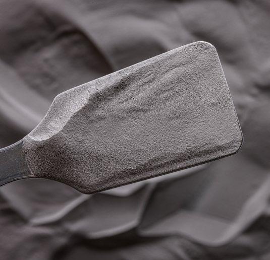
“So, what can be done with this unwanted, used powder without it creating larger and larger stocks of dangerous waste? The answer is being provided by the likes of Carpenter Additive and 6K Additive which have introduced schemes to take back scrap from their customers.”
condition of the powder is not being considered and the used powder is simply any portion that is removed from the machine at the end of any particular production period or batch.
So, what can be done with this unwanted, used powder without it creating larger and larger stocks of it? The answer is being provided by the likes of Carpenter Additive and 6K Additive, which have introduced schemes to take back scrap from
their customers. Here, scrap can also mean failed builds and support structures, as well as the used powder that may have been recycled in the process too many times. It can also include the balance of larger batches that cannot be mixed with other virgin powder. This can amount to tonnes of powder that the companies can immediately reprocess back into useable powder for those same customers.
Metal Additive Manufacturing | Spring 2024 137 Vol. 10 No. 1 © 2024 Inovar Communications Ltd | contents | news | events | advertisers | website | newsletter | GETPDF
Fig. 8 Spherical Ti-6Al-4V powder developed by IperionX for use in AM and other processes (Courtesy IperionX)
Sustainability and metal powders for AM
“6K Additive’s Bradshaw stated, “The environmental, economic and national security benefits means that using scrap to produce high-quality AM powder is the future.” This touches on something that makes a lot of sense and may become key to the success of using scrap materials for powder production in AM: national security. ”
These returned powders can be used along with primary metal feedstock or mixed with other pieces of scrap metal. The advantage here is that the powder can fill up those spaces in between the lumps of metal and improve the efficiency of the melting process, whilst also enabling producers to have fuller operational loads. In return for the revert powder, these suppliers offer favourable pricing on newly purchased powder (e.g. 6K Additive offer up to a 20% discount to its existing customers for selling scrap from the AM process.)
The future sustainability of AM with metal powders
Metal AM offers unique ways to be more sustainable, from how parts are produced to the materials used to make them. Metal powders are the most common feedstock for these processes, and it’s certain that if the world is to reduce carbon emissions and protect the environment, then we must use those materials responsibly and in ways that minimise resource extraction from the planet. Luckily, the economic drivers are very potent, so there can be no doubt that the re-use of powders in metal AM is going to increase. It is easy to see why, since Powder Bed Fusion
machines are already being used in significant numbers and at increasing sizes.
In any size of PBF machine, more often than not, the ratio of used powder to built part is quite high, and it is the cost of that powder that dictates whether it should be reused. Several tonnes of powder are required to complete a full build in the very latest large-scale, multi-laser machines. Imagine only being able to use all that powder just once! For AM to remain sustainable as the industry grows, there will have to be systems to collect and recondition that powder efficiently. In line with this, if that powder were to be returned to the original supplier, they should have all the means to test and qualify the composition and guarantee that it's the same quality of powder after being reprocessed.
In light of this, it’s not difficult to understand why companies like 6K Additive are investing in this particular area of the supply chain, and one can imagine many more companies entering this space in the near future. However, other technologies that have been in existence for decades can also be turned to reprocessing used powders. A good example of this was highlighted in the spring edition of Powder Metallurgy Review [6], where Phoenix Scientific Industries (PSI) Limited talked about Fluidised Bed
Reactors (FBR) and how they can be used “where batches of powder may need to be ‘rejuvenated’ or brought back into specification.” However, the problem with reprocessing used powder is that it still requires a lot of transportation, putting it at odds with emissions reductions.
Addressing this aspect of sustainability are those companies that have brought the capability to atomise smaller batches of powder to market, especially those where any feedstock – including scrap – can be used. Here, it’s feasible to have a system taking AM build waste and atomising powder at the end of the AM production line. It is certainly something that could be expected in companies that prefer fully vertically integrated processes.
6K’s Bradshaw stated, “The environmental, economic and national security benefits means that using scrap to produce high-quality AM powder is the future.” This touches on something that makes a lot of sense and may become key to the success of using scrap materials for powder production in AM: national security – not security threats and risks of violence, but supply chain security. Scrap materials sourced within any given territory can be much easier to qualify and guarantee its pedigree. It’s very likely to be the case for specific metals that are of more value, either due to a particular single end-use application or because they contain elements that are intrinsically difficult to source (such as scandium, tantalum, yttrium, niobium, etc.)
Sustainability, in this sense, does not have the environment as its main concern, but it does still have positive outcomes for the environment. Recent projects from the US Department of Defense and the UK Ministry of Defence are enabling companies like 6K Additive and Additive Manufacturing Solutions Ltd to investigate the use of existing assets at end-of-life as qualified feedstock materials for the production of powder. To some degree, this guarantees national supply chain security whilst also helping to
Metal Additive Manufacturing | Spring 2024 138 © 2024 Inovar Communications Ltd Vol. 10 No. 1 | contents | news | events | advertisers | website | newsletter |
Sustainability and metal powders for AM
fulfil commitments to international sustainability targets.
The work that is being paid for under the umbrella of defence does, however, show the way for all regulated industries. The medical, aerospace, automotive and energy sectors, for instance, have all spent significant resources over decades to develop materials. All those materials intended for the products of yesterday could very easily be the feedstock going into the products of tomorrow, especially since Additive Manufacturing means that those products are now being designed to be lighter, with greater efficiency and functionality, requiring less energy to run or utilise, and lasting much longer.
Author
Dr Martin McMahon Technical
Consultant, Metal AM magazine, and founder of MAM Solutions.
Martin.McMahon@MAMSolutions.uk
Acknowledgments
The author would like to thank the following companies for their most excellent contributions to this article:
6K Additive, Atomising Systems Ltd, Carpenter Additive, Circle Metal Powders Co. Ltd, Continuum Powders, ECKA Granules Germany GmbH, f3nice Srl, IMR Metal Powder Technologies GmbH, INDO-MIM Pvt. Ltd., Mimete Srl, Pometon spa, and Sandvik Osprey Ltd
References:
[1] R Bleischwit et al , Remaking steel for a net zero carbon circular economy, The Bartlett , www.ucl. ac.uk/bartlett/news/2021/sep/ remaking-steel-net-zero-carboncircular-economy
[2] M Kraft, Use of scrap metal in steel production significantly re-duces CO 2 emissions, Fraunhofer IMWS, www.imws.fraunhofer.de/ en/presse/pressemitteilungen/ scrap-metal-reduces-co2
[3] ArcelorMittal to produce steel powders for Additive Manufacturing industry, www.metal-am. com/arcelormittal-to-producesteel-powders-for-additivemanufacturing-industry/
[4] A Sanchez-Valverde Erice, Outokumpu: Bringing a new dimension to Additive Manufacturing with stainless steel powders, PM Review Vol. 12 No. 3, Autumn 2023, www. pm-review.com/wp-content/ uploads/2023/09/PM-ReviewAutumn-2023.pdf
[5] First plant in Europe to produce aviation-grade titanium by recycling, www.metal-am. com/first-plant-europe-produceaviation-grade-titanium-recycling/ [6] W Hopkins, From powder modification to rejuvenation: Fluidised Bed Reactors in metal powder production and Additive Manufacturing, PM Review Vol. 13 No. 1, Spring 2024, www.pm-review.com/ wp-content/uploads/2024/02/ PM-Review-Spring-2024.pdf
Metal Additive Manufacturing | Spring 2024 139 Vol. 10 No. 1 © 2024 Inovar Communications Ltd | contents | news | events | advertisers | website | newsletter | GETPDF
Sustainability and metal powders for AM


NORTH AMERICA’S LARGEST ADDITIVE MANUFACTURING AND INDUSTRIAL 3D PRINTING EVENT JUNE 25-27, 2024 Los Angeles Convention Center ADVANCE YOUR CAREER IN ADDITIVE SAVE $125 Claim Your Free Expo Pass & Save 25% on Conference Passes Register by May 15 With Code: RPMS REGISTRATION IS OPEN rapid3devent.com Your Full Conference Pass gets you access to over 160 presentations, across 14 subject tracks, over three days. Learn advanced AM insights from experts at: • Boeing • Glidewell • Google • GM • Mayo Clinic • Northrop Grumman • Rivian • Siemens • US Air Force • Zimmer Biomet
Inside Wayland Additive: How innovation in electron beam PBF is opening new markets for AM
UK-based Wayland Additive is convinced that, when it comes to metal Additive Manufacturing, Electron Beam Powder Bed Fusion (PBF-EB) has a bright future ahead. Whilst laser-based PBF is the most widely commercialised AM technology, it has inherent limitations that electron beam-based innovations such as Wayland’s NeuBeam process promise to overcome. Rachel Park reports on how the technology could open up the AM market by enabling users of the Calibur3 machine to rapidly develop and commercialise a wider range of industrial materials.
Metal AM magazine has, periodically, considered where Electron Beam Powder Bed Fusion (PBF- EB) processes fit within the metal Additive Manufacturing industry. Specifically, two articles by Joseph Kowen deftly sketched out the landscape in this regard in 2020 and 2022 [1,2]. In the latter article, Kowen concluded, “Progress in PBF-EB is measured but real, though there is much left to be done. The technology and its industrialisation are on track, but the game is long.”
Now, in 2024, Kowen’s conclusion continues to ring true, even as further progress has materialised both from the leader in the field, GE Additive, and a host of commercial newcomers in the field highlighted in the 2022 article, one of these being Wayland Additive.
Recently, Metal AM magazine’s Managing Editor, Nick Williams, and freelance writer Rachel Park visited the company to speak with key personnel about its electron beam metal AM process, NeuBeam, and tour the facility that produces the commercially available Calibur3 machines.
To understand the company's intent, it is important to get a handle on the unique aspects of its process. For this, Ian Laidler, Chief Technology Officer at Wayland Additive, and the lead scientist who proved the concept of NeuBeam for an Innovate UK-funded project in 2016, is best placed to explain.
“Electron beams have been used for decades in precision welding, in scanning electron microscopy and the semiconductor industry,” he stated. “The latter is actually my background. When we first looked at how electron beams were deployed for AM, at the time there was only one option, and the lack of stability struck us,
Metal Additive Manufacturing | Spring 2024 141 Vol. 10 No. 1 © 2024 Inovar Communications Ltd | contents | news | events | advertisers | website | newsletter | GETPDF Wayland Additive
Fig. 1 Wayland Additive's headquarters in Huddersfield, is located between the industrial cities of Manchester and Sheffield, in the north of England (Courtesy Wayland Additive)
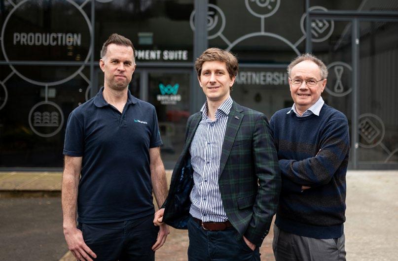
exhibited both in the machines and the output with a distinct lack of repeatability from part to part.”
Laidler’s overview of the PBF-EB process, compared with both the original PBF-EB manifestation and with Laser Beam Powder Bed Fusion (PBF-LB), offers an interesting insight into Wayland’s motivation. “Looking at all metal PBF technologies, each of the two competing energy sources –lasers and electron beams – brought their own unique challenges for
users looking to achieve successful outcomes. With the PBF-LB process, the machines are certainly more developed, but there are still limitations such as residual thermal stress, process emissions, low productivity, limited part volume and limited process control parameters. All of these restrict the process dynamics and the optimisation options that are available to the user."
“Today, the OEMs of laser-based AM machines and their customers
“...investment is being poured into the industry to try and develop ‘forgiving’ materials in order to get around the issues presented by both processes. This may be one way of solving the problem, but the strategy of relying on bespoke alloys for targeted applications only adds further costs...”
are turning to materials scientists to develop new materials specifically for the AM process in an attempt to overcome these limitations,” he continued. “Indeed, significant investment is being poured into the industry to try and develop ‘forgiving’ materials in order to get around the issues presented by both processes. This may be one way of solving the problem, but the strategy of relying on bespoke alloys for targeted applications only adds further costs for production applications.”
But let’s return to the overarching challenge of PBF-EB, powder charging, whereby process stability is immediately compromised.
The physics is important
An electron is one of the fundamental building blocks of all atoms that make up matter. Wayland’s Calibur3 machine – indeed all PBF-EB machines – harness the natural properties of electrons to produce a
Metal Additive Manufacturing | Spring 2024 142 © 2024 Inovar Communications Ltd Vol. 10 No. 1 | contents | news | events | advertisers | website | newsletter | Wayland Additive
Fig. 2 From left: Martyn Hussey, Head of New Technologies; Will Richardson, Chief Executive Officer; Ian Laidler, Chief Technology Officer (Courtesy Wayland Additive)
very high-energy, narrow beam that can melt metal. The most important property of electrons for Wayland is the negative electric charge that each electron carries; this permits the beam to be given very high energy, far in excess of the energy of a single laser in PBF-LB. This beam can scan at mind-boggling speeds and is able to be highly focused.
However, this negative electric charge also presents a problem when the electron beam strikes a bed of metal powder. The outer surface of each metal powder particle has a very thin layer of material that has reacted with the oxygen in the air – this layer is electrically insulating, meaning the electrons stick to the outside of the powder particle. This electron charge build-up on the powder can physically move the powder, thereby leading to a so-called ‘smoke’ event, or a rapid ejection of powder from the stable layer required to produce an AM part.
Obviously, it is not good when a smoke event occurs; the build process is invariably stopped and the AM machine may require a lot of time and attention to get it manufacturing again, reducing productivity considerably. The original PBF-EB process sought to overcome this instability by scanning the beam over the entire powder bed and sintering all of it to make it electrically conductive, thus preventing negative charge build-up, before applying higher temperatures to build the part by fully melting the layers in the specified geometry.
This original process led resultant parts to be caked in sintered powder, requiring intensive post-processing to remove the parts from the partly solidified material encasing them. This additional post-processing step is messy, labour-intensive, and adds further considerable cost to the bottom line of PBF-EB. There is, of course, also a risk of increased material waste.
These challenges, resulting from the inherent nature of electronic charge, have contributed significantly to PBF-EB lagging behind the more commercially successful laser-based metal AM technologies.
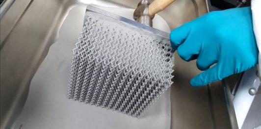
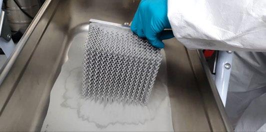
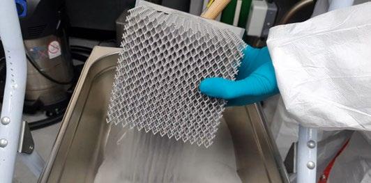
Laidler, however, believes that the physics of the electron beam process is actually ideally suited for AM. As a result, the Wayland approach to PBF-EB comes at the challenges from a completely different angle.
A stabilising force in electron beam AM
Laidler and his team of physicists developed a way of neutralising the build area by introducing a stream of positively charged ions to the build
chamber, under vacuum, to stabilise the process. This neutralised beam process – hence ‘NeuBeam’ – is capable of reaching very high temperatures in a more precise way, meaning it is a ‘hot part’ process, not a ‘hot bed’ process (the latter being how PBF-EB is often negatively characterised). The result is large amounts of free-flowing powder around the parts post-build (Fig. 3).
This offers two major advantages: a light sintering of the powder bed only happens locally to the part, thus resulting in less extensive
Metal Additive Manufacturing | Spring 2024 143 Vol. 10 No. 1 © 2024 Inovar Communications Ltd | contents | news | events | advertisers | website | newsletter | GETPDF Wayland Additive
Fig. 3 Free-flowing powder around a lattice part post-build is in stark contrast to the typical sintered powder 'cake' associated with PBF-EB (Courtesy Wayland Additive)
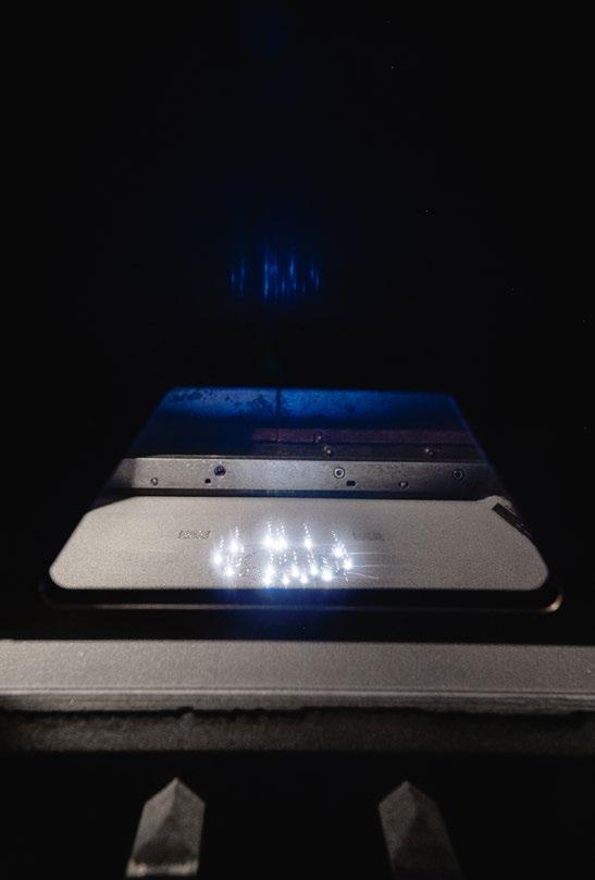
“An electron beam moves much faster than a single point laser – even if you have four, six or twelve lasers. With NeuBeam, we can have thirty-two to sixty-four simultaneously active melt pools. There are no laser metal AM machines that have thirty-two lasers, let alone sixty-four.”
post-processing, and the ability to process a much wider range of materials, including tool/carbon steels and reflective metals that have traditionally been avoided by laser and electron AM processes. These are both big deals, as anyone using metal AM machines will testify.
Martyn Hussey, Head of New Technologies and one of the founders of Wayland Additive, works alongside Laidler, specifically on the Active Charge Neutralisation approach. Hussey went further in detailing how the physics works. “It cannot be overstated that a metal powder bed is a very poor electrical conductor,” he explained. “By flooding the build chamber with a shower of positively charged inert ions – a technique employed in other fields of commercial scientific instrumentation – the NeuBeam process is able to neutralise the charge on the powder thereby eliminating electron charge induced smoke events.”
This all sounds simple enough in principle but, as ever, the reality was anything but, and required considerable development to arrive at a workable, repeatable and reliable industrial process. This included the need to calibrate for the beam deflection caused by the presence of the argon ions, stated Hussey, who also emphasised the fact that NeuBeam is optimised to use argon rather than helium, the former being a gas that is more plentiful and cheaper.
Will Richardson, Wayland’s Chief Executive Officer, explained, “It’s important to understand that while other industry sectors have validated this technique, no one else anywhere in the AM industry has attempted Active Charge Neutralisation. However, managing the charge was just one part of the equation. The further challenge for our early R&D programme – now achieved –was incorporating this breakthrough into an industrial machine that would build parts reliably.”
He added, “Today, NeuBeam parts are all comparable with the original PBF-EB process in terms of density, fidelity, and surface finish.”
Metal Additive Manufacturing | Spring 2024 144 © 2024 Inovar Communications Ltd Vol. 10 No. 1 | contents | news | events | advertisers | website | newsletter |
Wayland Additive
Fig. 4 A Calibur3 machine in operation. With NeuBeam, users can have thirtytwo to sixty-four simultaneously active melt pools (Courtesy Wayland Additive)
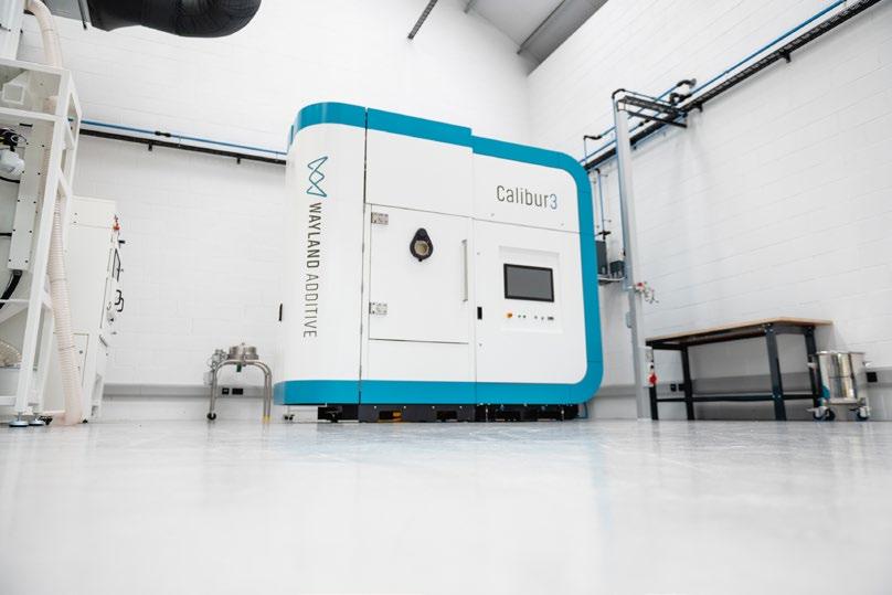
In addition to improved stability and loose powder benefits, other NeuBeam advantages also include a lower impact on powder morphology, lower radiation losses and no post-build heat treatment phase to de-stress the part.
This all means that with NeuBeam it is possible to rapidly develop parameters sets for new materials – on the fly, in some cases. Thus, customers and partners of Wayland can introduce new materials without a long, drawn-out empirical process. Crucially, these include materials that have never (or at least rarely) been attempted with AM, yet have been used for decades in other manufacturing processes.
Another positive outcome is that NeuBeam increases productivity. The team gave the example of how it is much faster to build a lattice with an electron beam than it is with a laser. Richardson stated, “An electron beam moves much faster than a single point laser – even if you have four,
“What this all means is that, with NeuBeam, it is possible to rapidly develop parameter sets – on the fly, in some cases – for new materials.”
six or twelve lasers. With NeuBeam, we can have thirty-two to sixty-four simultaneously active melt pools [Fig. 4]. There are no laser metal AM machines that have thirty-two lasers, let alone sixty-four. And they won’t any time soon.”
Opportunities beckon
From the interviews with the team, another distinct attribute of Wayland and its approach to the market became vividly apparent: Wayland is fully aware of the sector and its place
within it. When asked about how the company competes with PBF-LB, and the more established PBF-EB machine producers, the response from Peter Hansford, Chief Revenue Officer, was that, “in many ways, we don’t.”
Hansford explained, “Look, the laser metal AM processes are wellestablished, more mature, they have decades on the PBF-EB process, and so they are more advanced commercially – no one can deny that. The laser machines are very good at what they do with the materials that they have available to them. But directly
Metal Additive Manufacturing | Spring 2024 145 Vol. 10 No. 1 © 2024 Inovar Communications Ltd | contents | news | events | advertisers | website | newsletter | GETPDF
Wayland Additive
Fig. 5 A Calibur3 PBF-EB machine in the Production Suite at Wayland Additive is used on behalf of partners to run new projects (Courtesy Wayland Additive)
CUSTOMER PROFILE: Exergy Solutions focuses on large, high-wear AM parts
In 2021, Wayland Additive announced the first sale of its Calibur3 machine to Exergy Solutions Inc, Calgary, Canada. Exergy Solutions is an engineering consultancy offering end-to-end, fit-for-purpose lab- and pilot-scale equipment for research and innovation. The company operates in Calgary and opened its X-Lab in 2019, offering industrial AM and post-processing solutions, as well as a wireless augmented and virtual reality studio. Exergy works with clients in a variety of sectors including highly-regulated industries such as oil & gas, mining, manufacturing, and R&D.
The purchase by Exergy Solutions was supported by Next Generation Manufacturing Canada (NGen). “NGen’s mission is to support the development of unique, world-leading manufacturing capabilities in Canada,” stated Jayson Myers, CEO, NGen, at the time of the transaction. “It is investments like this that will enable our manufacturers to compete in the global marketplace and deliver the integrated engineering solutions that their customers need.”
Dr Dave Waldbillig, Director of Advanced Manufacturing, Exergy, commented at the time, “The investment in Wayland’s technology means that we can present a compelling solution to our customers’ wear challenges. The partnership combines the high wear resistance and toughness of the Vibenite series of materials from VBN Components, with the
larger build volume and speed of the NeuBeam process, and Exergy Solution’s application engineering support.”
“Exergy focuses on developing solutions for high-wear environments where complex geometries and large part sizes are needed for applications across many industry sectors, such as oil & gas, minerals processing, forestry, agriculture, pulp & paper, and power generation, among others. The Calibur3 metal AM system supports innovation for Exergy with its ability to process a wide range of materials in its large build volume, meaning we can focus on large footprint components.”
The Vibenite series of materials used by Exergy were developed by VBN Components, Sweden, and are characterised by the production of components with high fatigue resistance. This is due to the high carbide content, absence of porosity, and full hardness all the way through the component.
“The alliance between Exergy, Wayland, and VBN means that we are able to offer significant customer benefits,” concluded Billy Rideout, Exergy CEO at the time of the announcement. “With support from VBN, Exergy can now supply full-service design, manufacturing, and qualification support for large parts with complex geometries made from materials that are difficult or impossible to machine. This, in turn, means longer component lifetimes, with the entire part (not just specific areas of the part) made from highly wear-resistant materials.”
"Exergy can now supply full-service design, manufacturing, and qualification support for large parts with complex geometries made from materials that are difficult or impossible to machine."
competing with PBF-LB is not our focus today. Anyone that uses those processes, or is considering using them, knows that they do have limitations – every manufacturing process does, to some degree. What we are doing with NeuBeam is opening up new opportunities to work with unique materials, larger applications, and applications that have, in the past, required the significant use of support structures.”
Richardson went on, “Laser-based metal powder bed AM machines have dedicated markets and a good track record for producing lightweight, high-fidelity components with a high-quality surface finish. That’s well-known, but there are compromises involved. Companies that are using PBF-LB are using metals they can process on them, but they don’t tend to go outside of those bounds because it’s difficult."
“We’re often asked ‘why would a company use PBF-EB if they’ve got a laser-based machine?’: the answer is that NeuBeam reduces the need for compromise – both with traditional PBF-EB and with lasers. We are opening up new opportunities for existing PBF-EB users, for existing laser users, and for potential new users of metal AM that have steered clear of the technology because of all the challenges involved.”
Early NeuBeam adopters who have invested in a Calibur3 machine have identified new opportunities within their markets. To date, Wayland has sold and installed four machines and the company is on track to sell a further six this year. Hansford points to an impressive sales pipeline with increased sales targets for 2025 and beyond; they are not big numbers, certainly, but the strategy is measured, controlled and intended to support the installed machines while growing the customer base. Hansford explained, “It might be easy to focus on the ‘only four machines,’ but that is four industrial-scale machines installed and producing parts in four different materials. That is unprecedented in this industry, especially for a company that is still considered a start-up."
Metal Additive Manufacturing | Spring 2024 146 © 2024 Inovar Communications Ltd Vol. 10 No. 1 | contents | news | events | advertisers | website | newsletter |
Wayland Additive
“There are names on those six machines [in production] for this year, and conversations going on with regards to 2025,” he continued. “Virtually all of the pipeline customers are talking about different materials and developing original applications with them.”
Investment funding
What Wayland does very well –and, rather unusually, it must be said – is manage expectations both internally and with customers in terms of the process capabilities, the advantages offered, and how the tech is scaling up. Wayland is neither overselling the process nor itself. Rather, with its investors, partners and customers it continues to move forward with pragmatic goals. To date, it has delivered on promises and intends to keep doing that.
This approach has ensured steady expansion and growth by way of revenue generation (through sales and projects) as well as a consistent series of funding rounds. The latest of these rounds was announced in January 2024 with new investments from Parkwalk Advisors, Longwall Ventures and ACF investors, to scale up its operations further and expand its global customer base.
Parkwalk Advisors has supported Wayland since 2021 and invested £2 million as part of this round, which also includes long-term backer Longwall Ventures. With a total of £4.2 million already raised in the round, the company is continuing to talk to other investors that want to help the company build on its success and accelerate its vision. This followed a £4.6 million oversubscribed Series A funding round in April 2023, building on previous funding successes.
A realistic approach
Hansford believes that its realistic approach has contributed to Wayland’s success. “During the last four and a half years, as well as funding, we’ve successfully raised
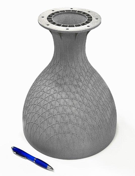
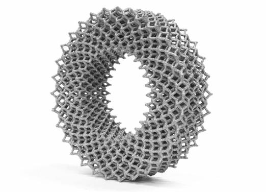
Metal Additive Manufacturing | Spring 2024 147 Vol. 10 No. 1 © 2024 Inovar Communications Ltd | contents | news | events | advertisers | website | newsletter | GETPDF
Fig. 7 A tungsten lattice part produced on the Calibur3 machine (Courtesy Wayland Additive)
Wayland Additive
Fig. 6 A 330 mm x 280 mm double skinned rocket nozzle mock-up, produced in Ti-6Al-4V with no supports and no requirement for post-build stress relief, on a Calibur3 machine (Courtesy Wayland Additive)
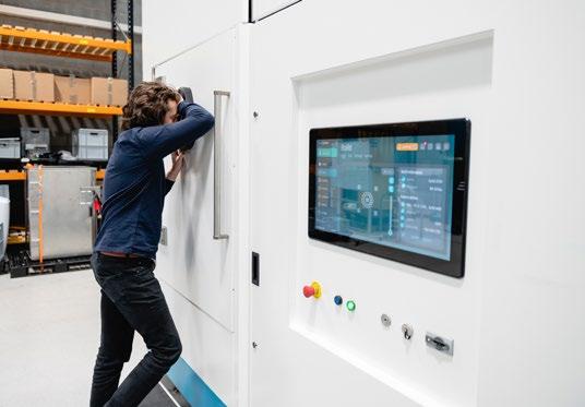
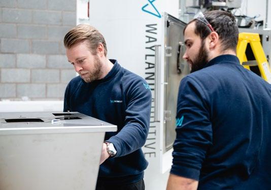
"...existing applications for PBF-LB tend to be smaller parts, with thin walls to cope with residual stresses. Laser processes are great at this type of application – we’re not trying to compete with that. However, NeuBeam can accommodate larger, bulk titanium parts, and that’s our USP."
aw areness that there is an alternative electron beam technology with new opportunities. We also took an early decision that Calibur3 would be an open platform. Wayland is not a materials supplier, and we are completely open to developing new materials and parameters in partnership with our customers. This means that we are not selling a locked down box that can only run approved materials; the machine is open and flexible, which allows much faster materials R&D.”
The most recent sale was to an unnamed company in continental Europe. That company went on to report to Wayland that it was able to develop a new material parameter set in an eight-week period and is already producing parts with the desired geometry in carbon steel.
Laidler commented, “We can work with our customers in this way because we believe that our machine offers greater flexibility and stability: this means that we can ‘let our customers loose’ to explore the potential of the technology.”
He continued, “Where we do overlap with laser powder bed machines is with titanium. Existing applications for PBF-LB tend to be smaller parts, with thin walls to cope with residual stresses. Laser processes are great at this type of application – we’re not trying to compete with that. However, NeuBeam can accommodate larger, bulkier titanium parts, and that’s one of our USPs, that’s where we’re also getting interest.”
Asked how they perceive their PBF-EB competitors, specifically the news in the week of our visit that Sheffield University had just taken delivery of a Freemelt PBF-EB machine, the team remained relaxed. “The Freemelt machine is much smaller, priced around the £300,000 mark, and it is probably more suited to that environment,” stated Laider. “Besides, UK universities rarely have access to £1 million in funding for a single platform. Calibur3 is priced that way because it has been built for production.”
Metal Additive Manufacturing | Spring 2024 148 © 2024 Inovar Communications Ltd Vol. 10 No. 1 | contents | news | events | advertisers | website | newsletter |
Fig. 8 Activity in the R&D department at Wayland Additive. Business development and the fundamental science that continues to drive R&D run in parallel across the business (Courtesy Wayland Additive)
Wayland Additive
Hansford added, “Getting more people working with PBF-EB is only a good thing. Getting an electron beam AM machine into any university is good. Similarly with competition in the market – it’s really positive for PBF-EB to have five or so suppliers. We shouldn’t be concerned with that. We’ll sell on our own technical and commercial merits. It’s about building trust and a relationship to build something together. No one does this lightly, you do it because you have a need. We’re not just a machine manufacturer – we’re a partner.”
Beyond proof of concept
It can, perhaps, be too easy for people outside of the company to categorise Wayland as ‘just another start-up’, with the assumptions that come with that label. Wayland is certainly operating beyond the constraints of a typical start-up that is only four years into its journey. The team was keen to emphasise its dual commercial and core science approach.
Business development and the fundamental science that continue to drive R&D run in parallel across the business today. Even with machines out in the field, R&D continues apace to improve the NeuBeam process further, to open up new material parameter sets quickly and consistently, all while adding value for existing and new customers.
I posited the idea of NeuBeam being a ‘work in progress’ which got an all-round immediate and resolute “No!” from all of the team members present. The successfully working Calibur3 machines in the field were the evidence they used to support this position. It was a strong argument.
When I suggested ‘workable innovation in progress’ the response was more receptive. Laidler ran with it, stating, “Calibur3 works, it works well, but it can still be refined and improved. For example, current R&D is looking
CUSTOMER PROFILE: Expanding the range of AM applications at EWI
In May 2023, EWI Inc, headquartered in Columbus, Ohio, USA, completed its purchase of a Wayland Additive Calibur3 machine. At the time of the announcement, Mark Barfoot, Director of AM Programs at EWI stated, “At EWI, we identified the NeuBeam process and the Calibur3 system early on and recognised its potential for novel and exacting production applications of AM."
EWI is an established, independent engineering consultancy with advanced manufacturing technology resources dedicated to production process development and improvement. It has customers in numerous sectors including aerospace and defence, automotive, aviation, energy, consumer electronics, medical devices, industrial products, and heavy equipment.
Wayland will continue to support EWI, in part through a sustainable Mixed Reality (MR) service contract offering. Ron Aman, AM Senior Technology Leader at EWI stated at the time, “The team is very positive about adding Calibur3 to our existing metal AM processes at EWI and the
new capability – and capacity – it will add. This system will enable us to extend the range of metal AM applications that we work on with our customers in the US and across the globe. We are also extremely pleased with the option to purchase the advanced MR service contract with Wayland. Their innovative approach to service engineering means that we will have full access to all of the digital assets we need, whenever we need them; as well as being able to call on any Wayland experts in a meaningful way, without having to arrange visits and travel between the UK and the US.”
Wayland's Peter Hansford, Business Development Director stated at the time, “It is extremely satisfying to see this purchase completed for both EWI and Wayland. This purchase has highlighted the synergies that exist as well as the potential for EWI that Calibur3 affords. EWI is a pioneer with metal AM for advanced manufacturing applications and with the experience and expertise of Ron Aman and his team, I know it is only a matter of time before new and exciting applications emerge.”
"The team is very positive about adding Calibur3 to our existing metal AM processes at EWI and the new capability – and capacity – it will add. This system will enable us to extend the range of metal AM applications that we work on with our customers in the US and across the globe."
Metal Additive Manufacturing | Spring 2024 149 Vol. 10 No. 1 © 2024 Inovar Communications Ltd | contents | news | events | advertisers | website | newsletter | GETPDF
Wayland Additive
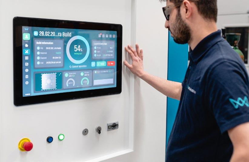
at extending the life of components on the machine and improving efficiencies in terms of energy and consumable gases. We are carrying out fundamental plasma physics research that is going to allow us to increase consumable lifetimes by more than 10X over the next couple of years.”
“I think we are original in the industry in that, normally, companies at this stage – four years in – are just launching machines and trying to sell them,” stated Hansford. “We
have a proven production process that we are continually improving. We have units sold and installed, we’re getting consistent positive feedback as well as listening to our customers on how they can be better and feeding that back into our R&D. Moving forward, we want our customers to be able to do things that they can’t do today. Our conversations are not about replacing or repeating but rather continuous innovation that allows us to grow into the marketplace.”
"...we want our customers to be able to do things that they can’t do today. Our conversations are not about replacing or repeating but rather continuous innovation that allows us to grow into the marketplace."
Laidler added, “I think our success comes down to a balanced combination of bravery and caution, plus some luck. You need all of them. First to know when to press ahead, second, to know when to push the brakes and reassess, and, well, you always need a bit of luck, too.”
Laidler went on to cite what he believes is one of the key enablers for the successful Wayland approach to R&D. “From the very beginning, we understood the benefits of incorporating in-process monitoring (IPM). Crucially, we developed our own IPM solutions and have intergrated them into our machines to better understand them. The aim being that, at the end of a build, we are able to identify every layer. Then, we put AI around that to identify optimum meltpool conditions, maintain them and ultimately keep the machine at optimum performance. This is turning into an effective USP of Calibur3, in that our users are able to define and characterise their parts with data post-build for verification, adding value for them.”
Metal Additive Manufacturing | Spring 2024 150 © 2024 Inovar Communications Ltd Vol. 10 No. 1 | contents | news | events | advertisers | website | newsletter |
Wayland Additive
Fig. 9 Calibur3's control interface (Courtesy Wayland Additive)
CUSTOMER PROFILE:
The Royal Air Force targets aircraft spares on-demand
In late 2022, Wayland announced the sale and installation of a Calibur3 machine at the Hilda B Hewlett Centre for Innovation, within No 71 Inspection and Repair (IR) Squadron, which is located at RAF Wittering in Cambridgeshire, UK.
The Hilda B Hewlett Centre for Innovation is the Royal Air Force’s first step into advanced component manufacturing. It is expected that the technology will provide a breakthrough in the RAF’s ability to design and produce its own aircraft spares on demand.
“The sale of our technology to the RAF is exciting for all involved,” stated Will Richardson, CEO at Wayland Additive at the time. For the RAF, spare parts can be produced using the Calibur3 system in days, not months – negating issues related to logistically challenging supply chains – at much lower cost, and without the need to stock an array of off-the-shelf spare parts.”
In addition to Wayland’s Calibur3 AM machine system, the Hilda B Hewlett Centre also has a Nikon XT H 450 scanner, a RenAM 500 metal AM machine from Renishaw, and a Stratasys Fortus 450 polymer AM machine.
Squadron Leader Allen Auchterlonie, Officer Commanding No 71 (IR) Squadron commented, “The aim of the project is for one day, the Royal Air Force to be able to manufacture structural aircraft components on main operating bases, or even in deployed locations. We’ll be able to save money, but more importantly, we won’t have to wait for spares to be delivered and we can get aircraft repaired far more quickly. The opening of this facility is a landmark in this exciting journey.”
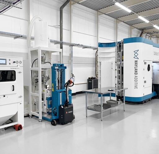
"Additive Manufacturing offers us enormous potential to repair and modify our aircraft quicker than ever before. Introducing any new capability into the RAF is a serious undertaking and the team at 71 Squadron has gone about this with professionalism and almost obsessive diligence."
71 (IR) Squadron is part of the RAF Support Force, and the previous Commander Support Force, Air Commodore Nick Huntley had commented at the opening of the facility that “Additive Manufacturing offers us enormous potential to repair and modify our aircraft quicker than ever before. Introducing any
new capability into the RAF is a serious undertaking and the team at 71 Squadron has gone about this with professionalism and almost obsessive diligence. This is a genuine milestone; a real achievement and I am proud that this project has been led by the Support Force.”
Metal Additive Manufacturing | Spring 2024 151 Vol. 10 No. 1 © 2024 Inovar Communications Ltd | contents | news | events | advertisers | website | newsletter | GETPDF
Wayland Additive
Fig. 10 Wayland Additive’s Calibur3 metal AM machine installed at the RAF's Hilda B Hewlett Centre for Innovation (Courtesy Wayland Additive)
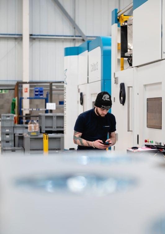
Company focus today
Wayland has grown and evolved as a company since it was founded as a commercial entity in 2019. At the start, there were fifteen core team members; today there are sixtyseven. Real estate has grown along a similar curve: nestled on a small industrial estate on the outskirts of Huddersfield, the team’s original headquarters in 2019 housed the R&D facilities with room to grow initial production capabilities.
In the four and a half years since, Wayland has extended its operational footprint into four further buildings on the same estate. R&D still resides in the original building, with additional R&D space, corporate offices, a dedicated production hall and a production suite all added.
The production suite is a custom-built facility housing a fully operational Calibur3 machine that can be used for or on behalf of partners to run new projects. Nearby, the production hall is an impressive set-up with a production line producing the next ten Calibur3 machines (Fig. 12).
"We have ten machines in production right now catering for orders at various stages of completion, some are approaching final testing and will go out for delivery this year. We have also got a strong stockpile with enough components for a further ten machines."
On the tour of the facility, we were introduced to Dan Rushton, Operations Manager at Wayland, who runs the production line logistics. Rushton stated, “We have six machines in production right now catering for orders at various stages of completion; some are approaching final testing and will go out for delivery this year. We have also got a strong parts stockpile with sufficient components for a further four machines this year.”
When asked about the facility itself, Rushton emphasised, “We have made significant investments in facilities and infrastructure over the last two years, more than doubling the size of our production facility as well as adding an inspection and workshop area. I have also overseen the installation of a large carousel where all machine parts are sorted and stored.
Back with the other members of the team in the production suite,
Metal Additive Manufacturing | Spring 2024 152 © 2024 Inovar Communications Ltd Vol. 10 No. 1 | contents | news | events | advertisers | website | newsletter |
Fig. 11 Calibur3 machines under construction (Courtesy Wayland Additive)
Wayland Additive
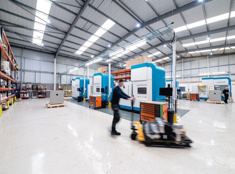
which also houses a conference room, Hansford indicated that the Huddersfield location works for the team, who have close ties with research and personnel at the Universities of Huddersfield and Sheffield. For this reason, negotiations have begun to build a new, larger facility that will bring all of Wayland’s operations together under one roof.
In closing, Metal AM magazine’s Nick Williams asked a rather challenging question: Given all this success and potential that we have seen today, will Electron Beam Powder Bed Fusion always be a niche AM technology?
Hansford was quick to take that challenge and provided a potent final thought to close out: “Every technology has its advantages and disadvantages. PBF-EB has dedicated markets that are excited. Yes,
it’s been slower to hit higher adoption rates – probably, at least in part, due to lack of competition and lack of innovation. Now it’s moving faster –but it’s never fast enough.
“All metal AM processes are really only just scratching the surface. New applications will continue to emerge as the scope of the technology, software and materials broaden. We are still in the early stages of metal AM, looking for the right size parts and the right materials. And, as ever, even with those identified, the economics have to make sense too.”
Contact
Peter Hansford Chief Revenue Officer
Peter.Hansford@waylandadditive.com www.waylandadditive.com
Author Rachel Park rachelp@rp-editorialservices.co.uk
References
[1] Unrealised potential: The story and status of Electron Beam Powder Bed Fusion, Metal AM Vol. 6 No. 2, Summer 2020. Read online: https://bit.ly/4a4pqUr
[2] Growing momentum and broadening recognition: A status update on the rise of Electron Beam PBF, Metal AM Vol. 8 No. 3, Autumn 2022. Read online: https://bit.ly/3V2PFqj
Metal Additive Manufacturing | Spring 2024 153 Vol. 10 No. 1 © 2024 Inovar Communications Ltd | contents | news | events | advertisers | website | newsletter | GETPDF
Wayland Additive
Fig. 12 Wayland Additive's production hall with the next ten Calibur3 machines in various stages of assembly (Courtesy Wayland Additive)

Put yourself on the right orbit and NETWORK AT THE WEST COAST’S LEADING SPACE SUPPLY CHAIN EVENT. Space Tech Expo USA is the leading showcase of technology and services for spacecraft, satellite and launcher systems, subsystems, components, and materials for civil, military and commercial space.


LONG BEACH california May 14-15, 2024
THIS IS
www.spacetechexpo.com
scan here scan here scan here scan here
300+ exhibitors // 40+ speakers // 2 conference stages
An end-to-end production case study: Leveraging data-driven machine learning and autonomous process control in AM
For Additive Manufacturing to mature as an industrial production process, believe Tommaso Tamarozzi (Oqton) and Juan Carlos Flores (Baker Hughes), it needs to be faster, simpler, and more reliable. This article reports on a step toward this goal through the development of an end-to-end AM workflow for the serial production of a Variable Resistance Trim (VRT) component. Built on a fully digital framework, it includes simulation, real-time process monitoring, anomaly analysis, and data preparation automation, thus laying the foundation for an AM workflow that delivers consistent quality and the documentation necessary for certification.
“You are just too young.” If one were to imagine a discussion between a personified CNC milling machine and a multi-laser Laser Powder Bed Fusion (PBF-LB) machine, this sentence would eventually come up. The CNC machine would point out the obvious problems that the brand-new metal AM machine is having. This would be unfair, however; milling and other subtractive manufacturing technologies have benefitted from a slow but steady evolution over the last century or so.
Metal AM has some way to go to achieve broad recognition as a value-adding process for a finite but broad variety of applications. The quality, repeatability, reliability, and traceability of the process are not currently at the level of subtractive manufacturing. It is difficult to achieve scalability in production or repeatability during fleet expansions, for example when opening new production sites. While significant steps have been taken to bridge this gap, it is fair to say that, historically, they have been sporadic, with multiple changes in sensor technologies, non-
standardised processes for quality, niche proprietary software solutions often targeting only single OEMs, and technology costs that are often too high to justify the investment. If we followed the argument of the CNC machine in the example above,
we would indeed need to wait for a greater level of technological maturity. However, we can and should continue to ask ourselves what are the key differentiators between additive and subtractive manufacturing. One could rightfully argue that metal
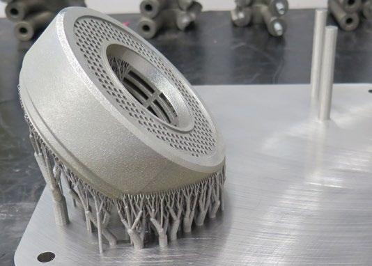
Metal Additive Manufacturing | Spring 2024 155 Vol. 10 No. 1 © 2024 Inovar Communications Ltd | contents | news | events | advertisers | website | newsletter | GETPDF An end-to-end AM workflow
Fig. 1 The Variable Resistance Trim (VRT) component used in this study, shown on a successful build plate with power supports and test specimens (Courtesy Oqton/Baker Hughes)
Example use case
Set-up of digital factory
Build preparation & anomaly prevention via build simulation
First build & in-situ build monitoring
Analyses, inspection & optimisation of first article
Serial production
Part deployment
Necessary technologies & industry-wide prerequesites
Cybersecurity
Physics-based simulation
The necessary actors and an application case: Baker Hughes VRT component
Generalisation & standardisation
Computational performance hardware & software
AI User experience
The general process proposed can be summarised in a few steps of an AM production infinity loop (Fig. 3) where a similar concept to a product lifecycle has been used. We will describe every step and dive deeper into the core technological aspects related to process monitoring and part inspection with examples. We will follow the path that energy technology company (Baker Hughes) and manufacturing software provider (Oqton) are taking to achieve an end-to-end workflow for the serial production of the VRT component shown in Fig. 1.
“To accelerate the mainstreaming of AM, we need to do something simple to describe but complex to achieve: establish an end-to-end traceability process covering both the physical and digital world...”
AM is a 'natively digital' process, which comes with its advantages. But, in short, while metal AM is 'too young,' it also has – on paper – the potential to leap through decades of trial and error by optimally combining all the technologies that are currently available.
If done in a smart, relentlessly organised, and pragmatic way, we believe that the future can be steered to a brighter place. The use case that we present here is meant to show that the relatively optimistic timeline described in a recent Metal AM magazine article [1] can be further reduced.
To accelerate the mainstreaming of AM, we need to do something which is simple to describe but complex to achieve: establish an end-to-end traceability process (covering both the physical and digital world) to minimise in-field failures, increase repeatability in (decentralised) production and guarantee that liability is assumed by the correct responsible actors if issues arise. And, while we are there, let us do it cost-effectively. Fig. 2 shows the workflow and the technologies needed to establish it.
This is a key component packaged in a valve body that provides a tortuous path configuration for a high-pressure drop liquid application. We will explore how Baker Hughes is working to maintain a high and repeatable production quality that its clients can easily certify. It also allows full history and traceability of the parts during the operating life of the component in case of malfunction or extraordinary maintenance.
The starting point is the assumption that one or more AM machines are installed at the manufacturer's facilities and that a part design is available. Here are the steps that need to be followed afterward:
1. Setting up a digital factory
The fundamental step of this process is to create a digital factory, or a digital replica of the shop floor. This digital twin needs to be integrated into the different enterprise systems so it works flawlessly from the order management perspective. This means that each AM machine gets a unique, digital version of itself containing essential information. Furthermore, each interacting member of an organisation is assigned a profile with the corresponding privileges and approval rights.
Materials, vendors, customers, processing, and post-processing
Metal Additive Manufacturing | Spring 2024 156 © 2024 Inovar Communications Ltd Vol. 10 No. 1 | contents | news | events | advertisers | website | newsletter | An end-to-end AM workflow
Fig. 2 The end-to-end quality and traceability workflow (Courtesy Oqton/Baker Hughes)

activities are also defined, and parts and orders are submitted through various demand generation, order management, and data integration systems. This set-up step is so important that it could merit an entire article [2], but, for the current case, let’s just assume that we have a digital factory and that orders and parts can be created and scheduled in advance.
2. Build preparation and first preventive actions via build simulation
Once the part design is available, we need to set up the build workflow with the corresponding data structure for the first article. This step is also part of the quality and traceability process. We select the materials, machine and all the hundreds of process parameters typical in metal AM, optimise part orientation, semi-automatically create support strategies, and perform simulationbased corrections. The simulation will reveal the potential risk for
cracks, recoater crashes, unwanted shrink lines and overheating, and will suggest pre-deformation to achieve the desired dimensional tolerances.
Once the build parameters, supports, orientation, etc. are optimised and satisfactory slicing is performed, build files can be created.
The VRT component built was optimised and simulated in 3DXpert, Oqton’s industrial Additive Manu -
facturing software. Fig. 4 shows the simulation results after a mechanical and thermal analysis.
At this stage, a connection to step 1 is created, each part is assigned a unique ID, and relevant files and metadata – including simulation summaries – are uploaded to the digital factory. A unique tie between the build prep information and the corresponding virtual part
“The simulation will reveal the potential risk for cracks, recoater crashes, unwanted shrink lines and overheating, and will suggest pre-deformation to achieve the desired dimensional tolerances.”
Metal Additive Manufacturing | Spring 2024 157 Vol. 10 No. 1 © 2024 Inovar Communications Ltd | contents | news | events | advertisers | website | newsletter | GETPDF An end-to-end AM workflow
Fig. 3 Infinity loop of metal AM production cycle – the digital world to the left and the physical world are continuously updating and improving each other (Courtesy Oqton/Baker Hughes)
Build preparation Update digital factory Product optimisation Build first article Inspect first article Serial production Monitor production Build simulation DIGITAL WORLD PHYSICAL WORLD DEPLOYMENT & OPERATIONAL LIFE DIGITAL FACTORY SETUP Optimise first article if necessary
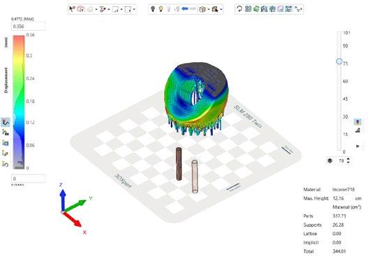
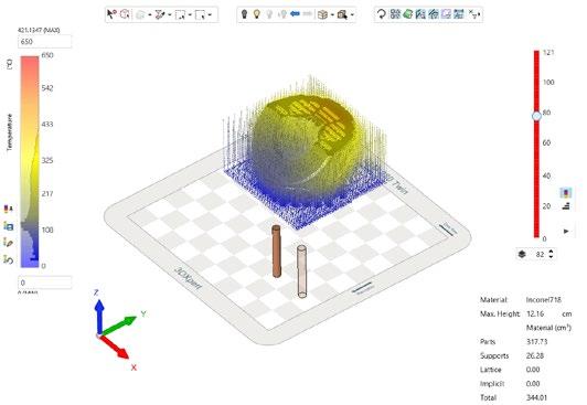
“This AI-automated audit monitor process releases significant specialised talent from repetitive routines and tedious work, although if necessary they can also monitor remotely the growth or self-correction of anomalies – intervening when deemed necessary.”
and order is established. Now we have both a physical and a digital factory and a virtual part with all the information needed for manufacturing. We can also evaluate the preventive work done to achieve the desired quality.
3.
Building the first articles and in-situ monitoring
The AM machine is instructed to build a component under the expert supervision of manufacturing engineers, workshop managers, and operators. The physical AM machines are securely connected to the digital factory using a gateway – an industrial computer with connectivity and computational capabilities (see next section).
The AM machine is streaming both IoT and camera image data to an Oqton gateway where the analyses are done in-situ and in realtime. This data analysis will reveal process deviations and operators will receive an alert in case the set-up thresholds are exceeded. Artificial Intelligence (AI) plays an important role in image processing for anomaly detection. Operators can be informed via email or directly on the cloud dashboard about possible anomalies. This AI-automated auditing process releases significant specialised talent from repetitive routines and tedious work, although if necessary they can also remotely monitor the growth or self-correction of anomalies– intervening when deemed necessary.
Fig. 5 shows the dashboard displaying the anomalies of an early test of the VRT while Fig. 6, left, shows an early prototype with anomalies caused by a non-optimised support structure.
Once the first article has been built, a very compact summary report is created and automatically linked to the virtual part in the digital factory.
4. Analysis and inspection of the first item
Given the importance of the VRT component and the foreseen production amount, we need to analyse the anomalies results file that was generated after the build. The results can be exported and opened in 3DXpert
Metal Additive Manufacturing | Spring 2024 158 © 2024 Inovar Communications Ltd Vol. 10 No. 1 | contents | news | events | advertisers | website | newsletter |
Fig. 4 Mechanical and thermal simulation of the VRT component (Courtesy Oqton/Baker Hughes)
An end-to-end AM workflow
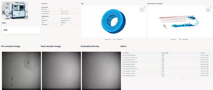

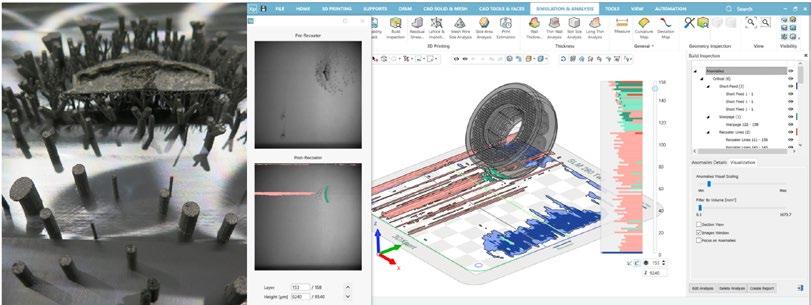
for further inspection. The distribution of anomalies over the build – their size, criticality, location, and possible correlation with, for example, simulation data and scan path – are performed, giving unique insights into the part quality and possible root causes (see Fig. 6, right.)
If the results are satisfactory, we can continue the production process. If the results aren’t satisfactory, the component might be scrapped and the design re-optimised, or sent for further Non-Destructive Testing (e.g., CT scan). It is recommended to do a CT scan of the first article regard -
less, which, together with the IoT and image anomalies analysis, gives us a comprehensive picture. A complete dataset for quality and comparison of the production part is now available. The summary report together with the connected data can now be considered as a 'golden set' and made available in the digital factory.
Metal Additive Manufacturing | Spring 2024 159 Vol. 10 No. 1 © 2024 Inovar Communications Ltd | contents | news | events | advertisers | website | newsletter | GETPDF
Fig. 5 Build monitoring anomaly detection and dashboard for the VRT example case (Courtesy Oqton/Baker Hughes)
An end-to-end AM workflow
Fig. 6 The result of a build with induced anomaly due to suboptimal support and 3DXpert Build Inspection analyses with pre- and post-recoater images, AI detection overlay for warpage and 3D aggregation with simulation overlay (Courtesy Oqton/Baker Hughes)
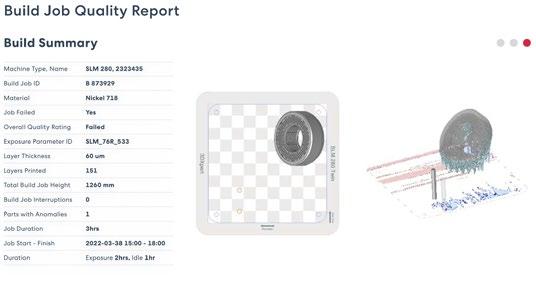
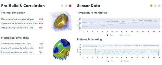
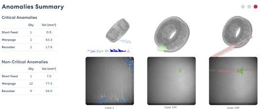
5. Serial production and possible de-localisation
Baker Hughes has multiple production facilities and may even use a qualified external vendor for serial production, decentralisation or localisation. For this reason, the company needs to be able to control the quality of its parts even when they're produced outside of its facilities.
Production facilities receiving production orders for the VRTs will also receive the required quality specifications, and be required to comply with the monitoring process and traceability that is aligned to the level of criticality of the to-be-manufactured component. Therefore, if a contractor carries out the production, Baker Hughes could monitor the compliance on the required specification directly online and/or simply receive a report. Details of post-processing steps, including inspection criteria, should also be traced and should be part of the digital twin factory setup. With this, each part can be evaluated as 'ready for deployment,' 'to be further inspected,' or 'to scrap'. Fig. 7 shows a summarised traceability report.
6. Deployment of parts
“Details of post-processing steps, including inspection criteria, should also be traced and should be part of the digital twin factory setup. With this, each part can be evaluated as 'ready for deployment,' 'to be further inspected,' or 'to scrap'.”
Finally, the parts are deployed into operation. In some cases, the produced parts might need to last up to thirty years in operation. For critical components, the full set of information contained in the streamlined preparation and quality report constitutes the must-go-to documentation to be used in case of auditing requests and/ or on-field issues in the future. When a problem arises, the engineering team will be in the best possible position and fastest route to analyse root causes, and quickly discriminate equipment faults, trace other components in other fleets at risk, and assess liabilities.
The technological prerequisites and blockers
Developing this end-to-end production integration came with certain technological challenges and requirements. We will analyse those challenges here
Metal Additive Manufacturing | Spring 2024 160 © 2024 Inovar Communications Ltd Vol. 10 No. 1 | contents | news | events | advertisers | website | newsletter |
Fig. 7 Summary of traceability quality report including build, simulation, IoT and anomalies information (Courtesy Oqton/Baker Hughes)
An end-to-end AM workflow
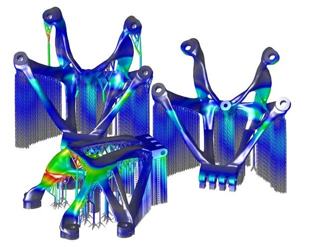
must (Courtesy Oqton/Baker Hughes)
with the intent to underline that if the devil is generally in the details – well, here the details are many, with all of the fine print typical to advanced technology. All stars and planets need to be meticulously brought into alignment to achieve successful end-to-end production.
1. Best-in-class physics-based computational technologies
Physics-based simulation sounds like it’s difficult to master. The end-to-end approach aims to allow AM experts to use simulation without being computational mechanics or finite elements experts. To speed up this process the use of models that can be used with simple-to-understand parameters that are 'good enough' should be used. The target is a balance between good predictive capabilities, ease of use, and sheer computational speed. The end-to-end approach leverages an extremely fast GPU-native voxel FE solver with automatic meshing that
“AI is not used here as a buzzword. Physics-based models are mostly deterministic and have great predictive capabilities, but AI models are good at detecting and bringing evidence to the fore based on real sensor information as input.”
focuses on the prediction of some anomalies, overheating and predeformation calculation. Fig. 8 shows a challenging simulation example with complex power-supports which can be run by non-experts when the correct technical choices are made.
2. Best-in-class AI models for anomaly detection and aggregation
AI is not used here as a buzzword. Physics-based models are mostly deterministic and have great predic -
tive capabilities, but AI models are good at detecting and bringing evidence to the fore based on real sensor information as input. In the end-to-end approach, we focused on branches of Machine Learning that are mature and industry-ready. We used image classification and segmentation with volumetric aggregation of topologically complex anomalies and validated it through a large development effort.
Metal Additive Manufacturing | Spring 2024 161 Vol. 10 No. 1 © 2024 Inovar Communications Ltd | contents | news | events | advertisers | website | newsletter | GETPDF
Fig. 8 Example of a complex mechanical simulation. The large amount of thin power support could drive the computational times to unreasonable values. Automation of element and mesh selection together with best-in-class GPU solvers are a
An end-to-end AM workflow
An end-to-end AM workflow
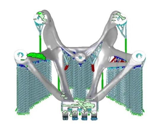
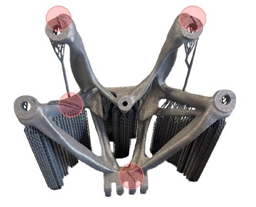
Once again, 'the devil is in the detail,' and here the details take the shape of the massive amount of data and images needed to train the AI models and the invaluable experience of partners like Baker Hughes and 3D Systems to steer the model in the right direction. Only cooperation between OEMs, AM experts, and software developers can have a chance of serious success. Fig. 9 shows one of the many validation examples for AI algorithm development.
3. Cybersecurity
In the end-to-end example of Baker Hughes’s VRT, the connection that tied the process is the underlying digital thread. In our case, this is centralised in the cloud-based Oqton Manufacturing OS. It’s easy to assume that data can freely stream from OT to IT networks to general-purpose cloud platforms such as Google Cloud or AWS without anyone raising an eyebrow. The reality is of course
different. Issues like IP protection, data leakage, external access to OT networks, etc. are paramount [3]. This is why Baker Hughes rigorously scrutinised the security of the solution through months of evaluation and cybersecurity tests.
4. Dataset standardisation, sensor availability, and machine agnosticism
If metal AM is to become a production method of choice, large and small players alike need to be able to use different equipment from different vendors. Because of the competition in the AM machine market, multiple OEMs are highly specialised in specific features and are particularly advanced for certain applications but might perform poorly on others. Customers want to start benefitting from this wide range of options, but the lack of standardisation is hindering them. This applies to sensors, (IoT) data types and communication protocols, specific proprietary software, and the openness of the AM machine’s software ecosystem for usage of the valuable streamed data.
Baker Hughes and Oqton made a conscious choice at the start of this project to focus on what is practical and feasible and not on what is theoretically optimal. Baker Hughes had invested several years in evaluating various monitoring systems with specialised high-end sensors and high-resolution with various multiphysics principles and had concluded that although one could develop a specialised system it was not practical, not scalable at an industrial level from the implementation perspective and the small, aggregated value did not provide a return for the investment.
We therefore used sensor data that is common to basically every machine (i.e., oxygen levels, pressures, temperatures, etc.) and optical images from standard cameras looking at the build plate and taken before and after the recoating happens. By optimally using this minimal set of data we can cover Baker Hughes’s portfolio
Metal Additive Manufacturing | Spring 2024 162 © 2024 Inovar Communications Ltd Vol. 10 No. 1 | contents | news | events | advertisers | website | newsletter |
Fig. 9 Example of validation between a build with anomalies and the detected anomalies using the AI strategy with volumetric aggregation (Courtesy Oqton/ Baker Hughes)
of large AM machines with a standardised set of information that can be used to compare and analyse part quality. The principle is that with this standard set of data, the overwhelming requirement is to have a high-end processing engine with robust AI and Machine Learning (ML) models with tens of thousands of trained images to generate the accuracy required to make concise operational decisions. The difference on this last approach is that once the models are trained and are machine and part agnostic then it is scalable and ready for an autonomous process, which enables AM at an industrial scale with a practical and economic solution.
This forms a strong basis to then further add sensors and information that the industry regards as important and avoids exotic and expensive sensors with uncertain added value.
5. Data size, real-time performance, and edge computing
While the set of information is the minimum required for a thorough analysis of quality, it can still be very large. This information also needs to be digitally stored, backed and possibly maintained with variable retention policies. Certainly, it also needs to be processed at a time that, for the metal AM application, can be considered real-time. In a matter of a few seconds – say up to twenty seconds – images of single layers need to be processed and run through the AI model, anomalies need to be aggregated considering all possible topological variations during the build, and IoT data need to be aggregated, synced, and eventually, streamed to a cloud tenant for visualisation and fruition. It goes without saying that 'every byte counts.' Advanced numerics need to happen on so-called edge devices or gateways – small industrial PCs with enough connectivity and computing power to ingest and elaborate data locally and relay only the relevant information.
In our end-to-end application, Oqton’s gateways played a crucial role. Even if the cloud solution is
“In our end-to-end application, Oqton’s gateways played a crucial role. Even if the cloud solution is not used, one still needs to create databases that are indexable and searchable through the years: storing and retrieving petabytes or more of data is not a viable option.”
not used, one still needs to create databases that are indexable and searchable through the years: storing and retrieving petabytes or more of data is not a viable option.
6. Ease of use
AM engineers, operators and shopfloor managers need to be allowed to do their job and not waste time on the intricacies of the underlying technologies. This end-to-end solution was developed with the aid of a strong team of UX designers focusing on ease of use for the problem at hand.
In short, all the above details need to be aligned for such a mature solution to be effectively developed, tested, and deployed – and for the end-user to benefit from it. This endto-end example shows that multiple players were needed to make this happen: Baker Hughes pushed the boundary to embrace a new fully digital paradigm, AM machine OEMs, such as 3D Systems and SLM Solutions, provided machine know-how and connectivity support, while Oqton provided the software. It is extremely important to understand that developing AM machines, developing software, and producing AM products are three very different businesses and each player needs to be optimally positioned to excel in their own skills. Anything else would be suboptimal.
An extended set of possibilities and applications
While the end-to-end workflow was showcased in the VRT use case, there are multiple benefits that such a complete solution can provide to other applications. Some of the most prominent are summarised here:
Where and when did the problem occur?
The above workflow was recently used to show that a crack on a component did not appear during the build process, but rather during a postprocessing step. This saved a huge amount of time and investigations on build preparation modifications.
Is it all scrap?
When a localised anomaly occurs, it can affect multiple parts. For example, a re-coater line can be caused by a small, localised deformation. The lack of powder on a straight line across the build plate can negatively affect other parts. Visual inspection after the build will only identify visible anomalies, but the part needs to be sent to CT or be scrapped if an internal wall is affected. The anomaly detection system allows us to partially recover large trays with multiple components if we discover that some of the parts are not affected by a critical anomaly.
Metal Additive Manufacturing | Spring 2024 163 Vol. 10 No. 1 © 2024 Inovar Communications Ltd | contents | news | events | advertisers | website | newsletter | GETPDF
An end-to-end AM workflow
Does the cause of part failure lie in the manufacturing process?
When one of multiple parts starts failing after a long time in service, how can we show that the manufacturing process is not the root cause? We trace every step of the production process and provide the information in an easy-to-read and easy-to-access report. From this, one can easily discard or further investigate slight deviations or potential risks highlighted during production. This reassures end-users and helps to properly assign liability. Comparison with similar parts or different instances of the same parts is a simple and effective way to eliminate doubts.
Act before it’s too late Today, some very large parts are being produced. Their cost is often very high and the machine and operator time expensive. By stopping a build early at the onset of an anomaly one saves time, material, and operator effort.
We can give many other use case examples, but this initial list of benefits which became apparent in the first deployments of the solution is a good summary of what to expect.
A bright future lies ahead
We strongly believe that this standardised end-to-end approach can bring clarity and significant added value in the streamlining of metal AM part development and production. It is a first step in helping the process to scale to the industrial
level of other mature manufacturing processes. This is just the beginning – but it is a very concrete and solid step, not just a promise of something to come in the coming years. It is 'here and now' and we can build from it and keep enhancing the process.
Of course, multiple steps need to be taken for the wider proliferation of such an approach. For this reason and to increase the endusers’ trust, the solution provided is modular and one can opt-in for just some of the features. The benefits of the full workflow will become apparent along the way. Technology development in AI, physics-based simulation, and combinations of the two with the advancements in cybersecurity and edge computing will pave the way for more useful extensions starting from a strong base. While sources such as [1] suggest a five or more years estimate for the technology to mature, we hope that this use case shows that the future is closer than expected. If we look a bit closer, it’s happening now.
Authors
Tommaso Tamarozzi
Product Director Additive Monitoring, Inspection and Simulation Oqton
www.oqton.com
Juan Carlos Flores
Executive Director, Additive Manufacturing
Baker Hughes
www.bakerhughes.com
References
[1] Atela, F. L., & Godfrey, D. (2023, Vol 9 No 4 Winter 2023). Mission possible: The five-year plan to gain FAA and EASA acceptance of in-process monitoring. Metal AM, pp. 147-152.
[2] Buttle, G. (2024, January 19). What is a Manufacturing Operating System? Retrieved from Oqton. com: https://oqton.com/posts/ whats-the-difference-between-amanufacturing-os-and-an-mes/
[3] Yampolskiy, M., & Kowen, J. (2023, Vol 9 No 4 Winter 2023). Cybersecurity in Additive Manufacturing: Securing the industry’s future. Metal AM, pp. 129-137.
Metal Additive Manufacturing | Spring 2024 164 © 2024 Inovar Communications Ltd Vol. 10 No. 1 | contents | news | events | advertisers | website | newsletter |
An end-to-end AM workflow
Americas’ Leading Conferences on Powder Metallurgy and Metal Additive Manufacturing are Coming to the Steel City!

PM, MIM, and Metal AM Tutorials

Carbide Technical Track
Daily Light Registration

Keynote Speaker: Damon West— “Be the Coffee Bean”





JUNE 16–19 • PITTSBURGH
Metal Powder Industries Federation APMI International For details, visit PowderMet2024.org or AMPM2024.org
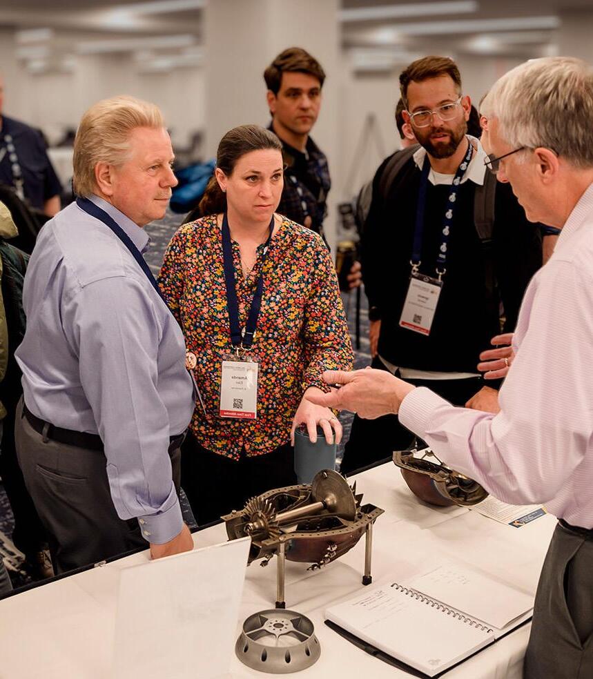

Additive Manufacturing Users Group March 30 - April 3 | Chicago 2025 AMUG CONFERENCE For Users. By Users. Engage, share, learn and connect. AMUG BUILDS THE EVENT YOU CREATE THE EXPERIENCE EDUCATION Technical, Panel & Keynote Sessions TRAINING Hands-on Workshops & Training Sessions NETWORKING Breakfast through Dinner COMMUNITY Users Supporting Users MarMark Your CalendarsPLasdfasdf AMUG provides the 3D printing experience everyone raves about. The AMUG Conference is where additive manufacturing users unite to share experiences and initiate collaborations. www.amug.com #AMUG2025 Mark your calendar for 2025
Consolidation, competition, and the cost of certification: Insight from New York's AM Strategies 2024
Additive Manufacturing conferences rarely attract as many industry CEOs as New York's Additive Manufacturing Strategies event, let alone persuade them to share the stage for panel discussions. AMS2024 was no exception.
On the back of a turbulent financial year for many of the industry's leading companies, how do those very CEOs see the state of the industry now, and what do they see as the biggest challenges ahead? Rachael DaltonTaggart reports for Metal AM magazine.
The seventh AM Strategies 2024 conference, organised by Additive Manufacturing Research and 3Dprint.com, was held in midtown Manhattan in New York City from February 6-8. This small but focused conference, with over a hundred speakers across three days, had a lot to offer. The focus, however, came down to three main topics: industry consolidation, what the industry is really in competition with, and the staggering cost of certification for Additive Manufacturing parts production.
With noticeably less hype from speakers than at many other conferences, and a seemingly genuine urge by key players to find ways for the industry to evolve, AM Strategies 2024 proved to be a unique event – and one to which I would like to return.
When considering the status of the AM industry, everyone acknowledges that it developed a financial wobble during 2023, with speakers attributing the Chapter 11 bank -
ruptcy of Fast Radius – which had $200 million in investments – in 2022 and its ensuing fire-sale acquisition by Sybridge for $15.9 million, as the first warning sign. Indeed, industry
analyst, Debbie Holton, pointed out to me during the conference that, since 2021, the total market capitalisation of the major Additive Manufacturing companies had dropped $54 billion
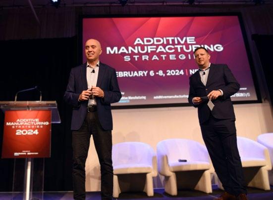
Metal Additive Manufacturing | Spring 2024 167 Vol. 10 No. 1 © 2024 Inovar Communications Ltd | contents | news | events | advertisers | website | newsletter | GETPDF AM Strategies 2024
person and Executive Editor, 3DPrint.com/VP of Consulting at Additive Manufacturing Research (Courtesy Ashley Alleyne/3DPrint.com)
in value since market highs in 2021, or an average of 80%, as of February 2024 (Table 1).
During 2023, the ongoing Stratasys saga – with Desktop Metal, Nano Dimension and 3D Systems levying bids – did nothing to boost confidence in the industry, with the months-long cycle of uncertainty and mud-slinging resulting in no mergers or acquisitions. Stock prices today remain noticeably low, and investors seem to be pausing. So, is this our new reality, or is the actual status of Additive Manufacturing better than the above suggests?
“Our industry is depressed,” said Asaid Yoav Zeif, CEO, Stratasys, during his keynote. “This cycle of stories [as described above] has caused people to lose confidence
2/8/2024
in the industry… but we are all still steadily growing. We will make it together. Our true competition is the status quo, and not within ourselves.”
Presenters agreed that growth continues despite investor caution. However, growth alone, among the individual companies, doesn’t solve the problems facing the industry. There are a lot of factors that need to evolve and be solved to ensure that market forecasts become a reality.
“I am optimistic,” said Terry Wohlers of ASTM and The Wohlers Report “But we have to be realistic and focus on the whole picture, which is good machines, good materials and not forgetting those very important workflows and proven applications.”
But even with the above in place, the situation in which many in the
AM industry find themselves is far from simple. “The relentless focus on growth and revenue [for the financial markets] leads to a situation where companies are not focused on overhead and gross margins,” said Brad Kreger, interim CEO of Velo3D.
Scott Dunham, Executive Vice President of Research, Additive Manufacturing Research, stated, “The cost of money, interest rates, inflation, and government responses to global conflict will account for a lot of activity in the market. But we see that AM is competing more and more against traditional manufacturing and we have to focus on that.” Above all, Stratasys’s Zeif stated, “We need to be profitable. We then need to use that to scale and scope across technologies.”
Metal Additive Manufacturing | Spring 2024 168 © 2024 Inovar Communications Ltd Vol. 10 No. 1 | contents | news | events | advertisers | website | newsletter | AM Strategies 2024
Table 1 Market capitalisation of publicly traded AM companies in February 2024 and at the 2021 peak (Courtesy Debbie Holton)
2021
Variance Publicly trade Additive Manufacturing companies Share price Market cap (M) Share price Market cap (M) Value % 3D Systems (DDD) $4.93 $657.80 $47.94 $6,871.00 $(6,213.20) -90% Desktop Metal (DM) $0.60 $194.40 $34.94 $7,590.00 $(7,395.60) -97% Stratasys (SSYS) $13.16 $910.20 $54.37 $3,078.00 $(2,167.80) -70% Nikon/SLM (SLM) $19.56 $4,311.00 $20.99 $6,394.00 $(2,083.00) -33% Velo3D (VLD) $0.27 $70.88 $12.71 $2,335.00 $(2,264.12) -97% Markforged (MKFG) $0.63 $124.30 $10.62 $1,978.00 $(1,853.70) -94% Materialise (MTLS) $5.64 $333.10 $80.62 $4,367.00 $(4,033.90) -92% NanoDimension (NNDM) $2.63 $617.20 $16.72 $3,506.00 $(2,888.80) -82% VoxelJet (VJET) $1.05 $9.59 $36.00 $196.46 $(186.87) -95% Sub-total $7,228.47 $36,315.46 $(29,086.99) -80% Protolabs (PRLB) $36.77 $948.10 $251.49 $6,734.00 $(5,785.90) -86% Xometry (XMTR) $33.25 $1,598.00 $87.39 $3,747.00 $(2,149.00) -57% Total $9,774.57 $46,796.46 $(37,021.89) -79% HP (HPQ) $28.26 $28,000.00 $34.32 $43,260.00 $(15,260.00) -35% Grand total $37,774.57 $90,056.46 $(52,281.89) -58% Fast Radius (FSRD) $15.90 $1,400.00 $(1,384.10) -99% 1.4B SPAC - sold for 15.9M $(53,665.99)
Peak
Consolidation is key
The Additive Manufacturing landscape has become increasingly complex. It used to be a fairly simple industry, with just a couple of AM processes and just a few pioneering companies but, by 2015, there were so many new AM processes being commercialised that ISO/ASTM created and published the seven types of AM identified by the standard ISO/ASTM 52900:2015 ‘Additive Manufacturing – General Principles – Terminology.’
Over the past ten years, however, the number of AM vendors has mushroomed further, and AM ‘variants’ have been invented beyond the original seven. As a result, some fear that the landscape is becoming confused and largely unfocused. Reminiscent of the car-making industry, there are voices stating that consolidation has to occur. Many seemed to agree that a reformation –disintegration and consolidation – of the industry is needed to get into mainstream manufacturing.
“The ability to scale matters,” said Ric Fulop, co-founder & CEO, Desktop Metal. “But we don’t yet have a billion dollar AM company in the industry so consolidation is needed.” Yoav Zeif added, “We must join forces to consolidate like other complex and capital-intensive industries, creating the scale needed for manufacturing. Consolidating will enable higher R&D investment, establish complete ecosystems and workflows, allow greater standardisation, and create an internal network effect enabling delivery of solutions across global conglomerates.”
But no one seems to be too clear on how that consolidation would occur. Would a merger of two major Additive Manufacturing companies be approved by the SEC? Maybe greater collaboration – without merger and acquisition activity – would be beneficial if it was done sincerely.
Collaboration is already a key to advancing the industry through activities such as the 5550 Common Additive Manufacturing Qualification Template (CAM-QT), being led by America Makes and ASTRO America.
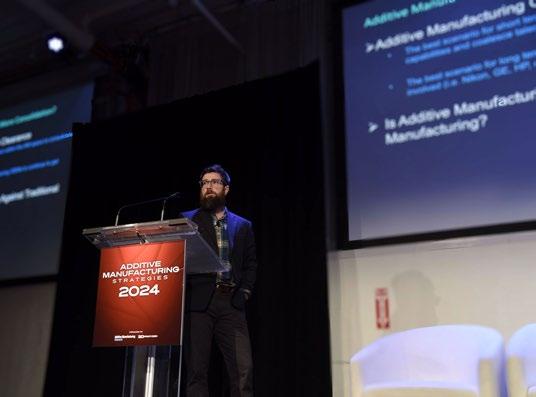
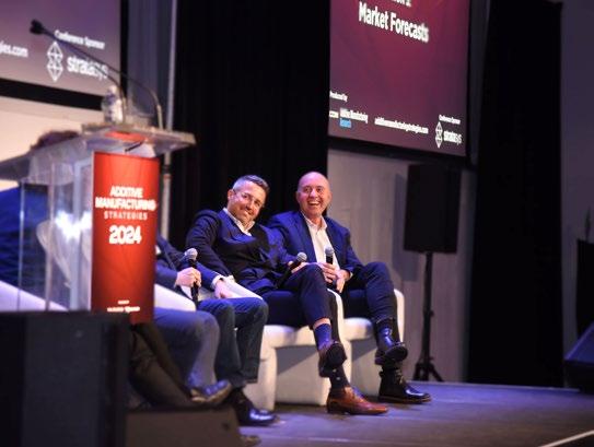
“Reminiscent of the car-making industry, there are voices stating that consolidation has to occur. Many seemed to agree that a reformation –disintegration and consolidation – of the industry is needed to get into mainstream manufacturing.”
Metal Additive Manufacturing | Spring 2024 169 Vol. 10 No. 1 © 2024 Inovar Communications Ltd | contents | news | events | advertisers | website | newsletter | GETPDF AM Strategies 2024
Fig. 3 Sam O'Leary, CEO, SLM Solutions, on stage with Stratasy's Asaid Yoav Zeif (Courtesy Ashley Alleyne/3DPrint.com)
Fig. 2 Scott Dunham, Executive Vice President of Research, Additive Manufacturing Research, speaking at AMS 2024 (Courtesy Ashley Alleyne/3DPrint.com)

that are more cost-effective than traditional manufacturing and additively manufactured in the region where there is demand. “In this case, experts have come together, including OEMs, to map out a regulated supply chain for ‘certified’ 3D printed automotive repair parts,” Dimovski stated. “Collaboration is a key to success in this.”
Certification and qualification: outdated?
Meeting certifications and qualifying machines, materials, parts and processes remain an expensive barrier to the more widespread adoption of AM – especially in metal. This is after achieving standard industry certifications such as ISO 9001 and quality standards such as SAE AS9100.
This effort is focused on trying to understand and define the common requirements of AM qualification from key aerospace industry OEMs. It is reliant on collaboration from GE, Honeywell, and Pratt & Whitney, so that there is a common core for contractors to work to for qualification, with a view to reducing costs and time for future qualification.
Mario Dimovski, Director of Innovation and Transformation, Boyd Group, 3D in Auto Repair, explained during the AM for Mobility panel that collaboration is the key to the 3D Printing in Auto Repair Task Force, led by IBIS Global. This effort is designed to provide a secondary solution for OEMs or parts suppliers who might need smaller part runs
“...there is serious concern in the US that arcane AM qualification requirements, especially in metals, mean that every machine, material, and part undergoes expensive test builds that are usually a cost to the parts supplier, not the purchaser. And this testing is not limited to the initial qualification stage...”
Indeed, there is serious concern in the US that arcane AM qualification requirements, especially in metals, mean that every machine, material, and part undergoes expensive test builds that are usually a cost to the parts supplier, not the purchaser. And this testing is not limited to the initial qualification stage either: testing has to continue throughout to ensure quality builds and any change of material or machine, even relocating a qualified machine requires requalification. “I talk to many metal AM producers and the big complaint is about the high cost of testing for qualification,” said Velo3D’s Kruger. “What are we able to do to reduce those costs?”
Additional testing requirements by prime contractors to the Department of Defence (DoD) mean that a Tier I/ II supplier using metal AM for aerospace applications has to go through the standard requirements testing such as NASA 6030, then engage in testing for each different aerospace OEM. Therefore if a supplier wishes to provide parts to three different prime contractors, they have to run three different test build results, tuned to their proprietary requirements, thus increasing costs. With such high costs of entry, many poten -
Metal Additive Manufacturing | Spring 2024 170 © 2024 Inovar Communications Ltd Vol. 10 No. 1 | contents | news | events | advertisers | website | newsletter |
Fig. 4 From left: Humna Kahn (CEO and founder, ASTRO Mechanical Testing Laboratory), Jonathan Cohen (CEO and founder, MIMO Technik), Jeffrey Gaddes (Additive Manufacturing Subject Matter Expert, U.S. Army), and Gina Ghiglieri (Additive Manufacturing Manager and Subject Matter Expert, Maxar Space) (Courtesy Ashley Alleyne/3DPrint.com)
AM Strategies 2024
tial suppliers will now not attempt to provide AM parts to the US aerospace and DoD supply chain – places where AM can deliver such high value.
“The cost of certification for users can typically exceed the value of the contract in hand, especially when the OEM only needs a limited amount of parts,” said AM Research’s Dunham. “We have to work with the government to create a funding line that will pay down the cost of certification. But the data created also has to be made available.”
The lack of available data for qualification is an area that can be solved through better software to manage the process, which will, in turn, provide better, more automated traceability.
But it was also interesting to hear the younger participants in the industry — all founders of more recent startups — deliver a verdict on current requirements. “We have to mythbust AM qualification and the outdated standards and requirements attached to it,” said Humna Kahn, CEO and founder, ASTRO Mechanical Testing Laboratory. This was amplified by Jonathan Cohen, CEO and founder, MIMO Technik, who stated, “Repeatability and reliability of the machines remains an issue. But while we are fixing that through machines, materials and software, we are still being held back by outdated standards and outdated thinking.”
However, such standards and requirements are driven by concerns about part integrity and human safety, especially for critical parts in flight or on and under the water. Matthew Sermon, Executive Director for Program Executive Office for Strategic Submarines, US Navy, explained, “We are not backing off on safety with AM parts for submarines in any way, but this is a national security imperative, and we will have to figure it out, and we will have to fundamentally change the way we do this.”
But no one can yet provide an answer for reducing testing and qualification costs. “The only way to reduce the cost of testing is to do less of it,” explained Harshil Goel,
“...no one can yet provide an answer for reducing testing and qualification costs. 'The only way to reduce the cost of testing is to do less of it.”
CEO of Dyndrite. This, by extension, means that test builds must be done faster, and there must be a higher degree of part success out of the gate. Goel contends that only new-generation software can achieve this – especially under current requirements.
New advanced software such as Dyndrite can provide significantly faster Design of Experiments,
utilising and quickly testing hundreds of parameter settings (e.g. hatching, energy density, and thermal time) on a material and then building a recorded toolpath that can be repeated. This means test builds can be quickly refined programmatically, not manually, thus removing hours of manual 3D design and enabling quick resolution to ensure that a qualification build meets require -
Metal Additive Manufacturing | Spring 2024 171 Vol. 10 No. 1 © 2024 Inovar Communications Ltd | contents | news | events | advertisers | website | newsletter | GETPDF
AM Strategies 2024
Fig. 5 Harshil Goel, CEO of Dyndrite: "The only way to reduce the cost of testing is to do less of it" (Courtesy Ashley Alleyne/3DPrint.com)
“Consolidation is now the only way to achieve a profitable business. The industry needs to grow up. Many AM companies built a business but failed to build a working business model. Your machine can’t move forward without fuel, unless it’s heading downhill.”
ments. Recording these parameter sets means improved traceability and the ability to save and share the data with the right parties and other machines.
Many also believe the addition of Artificial Intelligence, or AI, can add power to that process. A start-up called AI Build promises to deliver intelligent tools that can scale AM processes through the automatic creation of workflows, supports, and toolpaths using process monitoring, thereby reducing build failures. But this still does not avoid the fact that each separate machine, material and part has to be qualified, regardless of model; that a software upgrade to a machine might not meet requirements and approval; and that requalification has to be performed.
Many companies, especially in metal AM, are working towards making qualification easier. Velo3D and IMI Global recently produced test results on the ability to build the same part, machine-to-machine, siteto-site without requalification. The key here is the ability to define and save build parameters and calibration instructions within the Velo3D equipment, replicate atmospheric conditions and produce consistent build quality. However, this does not bypass the current network of written requirements and qualifications specified by various associations or committees.
Time for the AM industry to grow up
AM companies have been competing amongst themselves to be recognised as leaders in this rather small, niche industry. A resounding theme through AM Strategies 2024 was the need to recognise the true competition: traditional manufacturing. To be part of this bigger picture, and compete with traditional manufacturing, the AM industry needs more reliable, repeatable applications.
“Market caps for AM companies were based on AM capturing the mainstream manufacturing markets,” said Dunham. “AM has been operating
Metal Additive Manufacturing | Spring 2024 172 © 2024 Inovar Communications Ltd Vol. 10 No. 1 | contents | news | events | advertisers | website | newsletter |
Fig. 6 Gregory Hayes Senior Vice President, Applied Technology, EOS Group, EOS North America (Courtesy Ashley Alleyne/3DPrint.com)
Fig. 7 Yoav Stern, CEO and Member of the Board, Nano Dimension (Courtesy Ashley Alleyne/3DPrint.com)
AM Strategies 2024
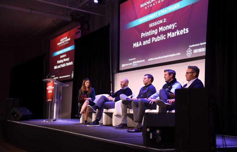
in a market that was parallel to traditional manufacturing. Now we have to compete fully against it.”
EOS’s Gregory Hayes agreed, stating that, “We need to stop competing within our echo chamber. We should be focusing on supply chain and delivering repeatable and reliable solutions. We must focus on maturing the technology.”
Yoav Stern, CEO and Member of the Board, Nano Dimension, added, “Consolidation is now the only way to achieve a profitable business. The industry needs to grow up. Many AM companies built a business but failed to build a working business model. Your machine can’t move forward without fuel, unless it’s heading downhill.”
All attending seemed to agree that it is time for AM to grow up, focus on the bigger manufacturing picture and develop solutions that deliver positive use cases – and do it now, together.
“Debbie Holton shared the Simon Sinek quote, ‘What got us here won’t get us there, and knowing who our worthy rivals are is the best way to help us adapt and improve before it’s too late.’”
After the dust has settled
AM Strategies 2024 was a fast-paced, intense conference. A lot was said, and many assertions made. There was even the faint promise of an industry that would work together more closely. But what does it all mean in the long run; what needs to be done?
Looking back at the event, Debbie Holton, manufacturing industry
analyst and consultant and a moderator at the event, said, “I think of the Simon Sinek quote, ‘What got us here won’t get us there, and knowing who our worthy rivals are is the best way to help us adapt and improve before it’s too late.’ This obvious maturity gap in the industry shows a clear need for consolidation and collaboration, but we have to move toward boring rather than sexy applications, and all are signals
Metal Additive Manufacturing | Spring 2024 173 Vol. 10 No. 1 © 2024 Inovar Communications Ltd | contents | news | events | advertisers | website | newsletter | GETPDF
Fig. 8 Moderated by Alex Kingsbury (Market Development Manager, Additive Manufacturing, nLIGHT), the Printing Money session featured Stephen Butkow (Managing Director, Cantor Fitzgerald), Arno Held (Managing Partner, AM Ventures), Bryan Dow (Managing Director, Cantor Fitzgerald), and Danny Piper (Principal, NewCap Partners, Inc.) (Courtesy Ashley Alleyne/3DPrint.com)
AM Strategies 2024
“We have all heard the hype about AM over the years. Now we are hearing industry leaders pontificate about how to re-centre the industry and return to profit and much bigger revenues. But I remain cynical; after all, money talks, especially with the current short-term focus on quarterly earnings.”
of a needed change. Do we have a long-term enough view to see it that way? Or are near-term quarterly market-cap valuations making us too myopic?”
The clearest thing in the industry may be that the path to industry success is not clear at all. However, as Fulop put it, “2024 is going to be a make-or-break year for AM.” The need for profitability and rolling some of that profit back into R&D leads to the aim of consolidation of some of the bigger companies in the industry.
However, will historically competitive companies be able to cooperate, combine and collaborate in the spirit of ‘a rising tide lifts all boats’ (per John F Kennedy) as suggested through AM Strategies 2024? Or will it turn into a ‘last man standing’ scenario?
“Focusing on the proper ‘rival’ is one aspect of future success,” said Holton. “And the rest will require some mature, long-term industrial leadership perspectives and ‘egochecking’ to truly industrialise AM. On my panel, Matt Sermon called it the ‘Manhattan Project’ for our time.”
Now what?
We have all heard the hype about AM over the years. Now we are hearing industry leaders pontificate about how to re-centre the industry and return to profit and much bigger revenues. But I remain cynical; after all, money talks, especially with the short-term focus on quarterly earnings. Will CEOs engage in more
altruistic and meaningful mergers and collaborations in this year than in years past? Are their boards and investors willing to bet on long-term industry prosperity over more immediate company revenues? Can AM enterprises do this themselves, or do they need neutral direction by the non-profits like America Makes, BlueForge Alliance and ASTRO America?
Maybe at the next AM Strategies event we can start to hold them to account – report back what each company has done, sincerely, for the growth of the industry and not just for revenue streams. That is where the true value of this event will come to the fore.
Author Rachael Dalton-Taggart CEO, AshBridge Media Consulting, LLC rachael@ashurstbridge.com
Rachael is a long-time veteran of the 3D technology industries, having reported and marketed MCAD, Reverse Engineering, and Metrology software, as well as traditional manufacturing and Additive Manufacturing technology. She now works as an industry researcher on projects designed to drive adoption and scaling of AM technologies into the supply chain.
Metal Additive Manufacturing | Spring 2024 174 © 2024 Inovar Communications Ltd Vol. 10 No. 1 | contents | news | events | advertisers | website | newsletter |
AM Strategies 2024
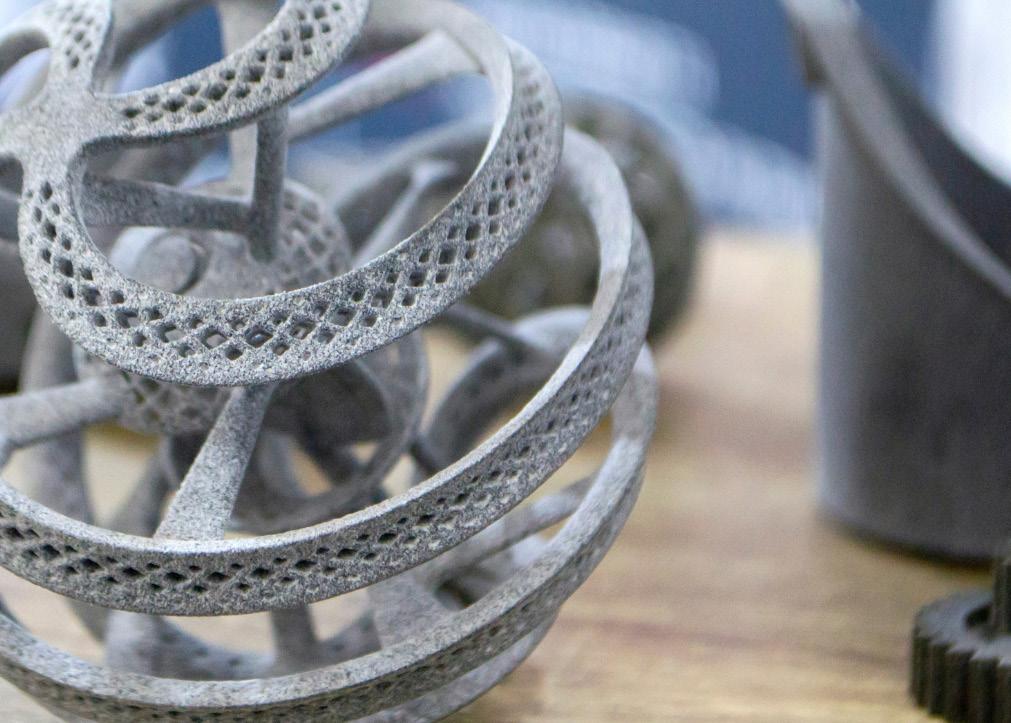
We Convene...
The most brilliant minds from industry and academia
We Coordinate... Transformative technical and workforce data
We Catalyze...
High-value, high-impact collaborative projects
America Makes is the leading collaborative partner for additive manufacturing and 3D printing technology research, discovery, and innovation in the U.S. Structured as a public-private partnership, we innovate and accelerate AM/3DP to increase global manufacturing competitiveness.
Focused on additive manufacturing, America Makes is the first institute of the Manufacturing USA® network.
Learn more at www.AmericaMakes.us



300
80
6
100


3D
The leading additive manufacturing trade show in France
CONGRESS/ EXHIBITION FORMAT
full-fledged connection platform to drive exchanges forward between actors of the additive
and
looking
A
A
manufacturing value chain
manufacturers
for innovative solutions.
printers, peripheral equipments,
softwares, 3D
design,
and
metrology... ...bigbang.frPhotographies © Nicolas RodetCe document est publi é par
Scan me to get your FREE access badge
explore the latest
in
and decipher the latest trends.
materials,
scanners,
prototyping
production services, post-processing, inspection,
3dprint-exhibition-lyon.com
to
innovations in additive manufacturing,
all materials and for all industries,
EXHIBITORS AND BRANDS
CONFERENCES AND WORKSHOPS
INTERNATIONAL SPEAKERS
000 PARTICIPANTS ANNIVERSA RY EDITION 10 Y E ARS
: « The 3D PRINT trade show holds a key position as the benchmark for additive manufacturing in France. »
: « 3D PRINT enables us to meet many new customers and prospects. »
HALBRONN
AIRBUS
Scandium's impact on the Additive Manufacturing of aluminium alloys
The future of Additive Manufacturing lies in part production at scale. Innovation must, therefore, focus on how to reduce part cost and improve performance. Unlike other manufacturing processes, weight is time in AM – and time is money; raw material costs take a back seat when it comes to overall part cost. Here, Jonathan Meyer (APWORKS) and John Barnes (Metal Powder Works/The Barnes Global Advisors) explore the case for scandium-based aluminium alloys for AM from both technical and economic perspectives.
In metallurgical terms, scandium forms a precipitate in solution with aluminium, but we digress. It is a solution because the Additive Manufacturing of aluminium alloys is facing ever more demanding requirements – both technical and economic.
The future of AM is in part manufacture, so innovation will increasingly be focused on how to reduce part cost and improve performance. The AM machine is an enabler: it enables new designs. Materials come into the frame to bring out the performance of the design. A lighter, lower-cost solution is achieved when these factors work in harmony. We both love applications, design, and materials and the amazing intersection that can emanate from them. We also love scandium and believe it is a solution for aluminium-based parts produced by AM.
We have written previously on the virtues of scandium-containing alloys of aluminium, specifically Scalmalloy® [1]. In that article, we generated a trade study looking at the overall part cost of an aluminium brake caliper traditionally manufac -
tured from machined 6061, additively manufactured from AlSi10Mg, Scalmalloy, and Ti6Al4V. That study asserted that Scalmalloy, despite the powder being three times higher in price versus AlSi10Mg, resulted in a significantly lower cost AM part.
This may seem to be an unexpected result but, due to the high cost and low productivity of AM machines, the cost of AM parts is heavily driven by the build time on the machine. This means that any weight saving in the part which can
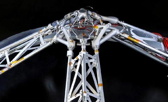
Metal Additive Manufacturing | Spring 2024 177 Vol. 10 No. 1 © 2024 Inovar Communications Ltd | contents | news | events | advertisers | website | newsletter | GETPDF
Scandium and aluminium PBF-LB
Fig. 1 Additively manufactured Scalmalloy thrust frame components (top centre of image), manufactured by APWORKS as part of an ArianeGroup GmbH technology demonstrator for the purpose of cryo-temperature and static loading tests, with funding from the German Aerospace Center (DLR) (Courtesy ArianeGroup/DLR/APWORKS)
Low volume prototypes
High complexity
High strength
High volume production
easily machined with high rates of material removal and relatively low tool wear.
This economic aspect limits the niche of applications where AM makes sense in aluminium to those geometries which cannot be machined and are in low volumes where die-casting doesn’t make sense.
Or does it? With a high-strength aluminium alloy, you can additively manufacture something which cannot be easily achieved by machining or casting, at any volume of production. This is the combination of high mechanical properties with the complexity of casting-type geometries. In applications where this combination of capabilities is valued, high-volume production of aluminium parts using AM can be viable.
be achieved due to improved material properties, results in a significant reduction in the production cost. In AM, weight is time and time is money. Raw material cost, which is a major input cost in traditional manufacturing, takes a back seat concerning overall part cost. This result exemplifies the role of design and material properties in the economics of Additive Manufacturing.
Today, aluminium AM represents a small percentage of the overall metal AM market, let alone the aluminium market. This is in part due to the current material offerings for the AM of aluminium compared to the marketplace of existing aluminium applications. Current applications made from cast or wrought aluminium start with raw materials priced from $2-10/kg, and which are
“In AM, weight is time and time is money. Raw material cost, which is a major input cost in traditional manufacturing, takes a back seat concerning overall part cost. This result exemplifies the role of design and material properties in the economics of Additive Manufacturing.”
Fig. 2 shows a Venn diagram, which highlights this niche. In the diagram, this may look like a very small niche, but in terms of economic volume, the market size for serial production of such parts is orders of magnitude bigger than the market for prototypes in aluminium. This is because the potential volume of parts to be produced in this niche is much higher, and we are talking about serial production, albeit of a small number of different parts where these properties are important.
Additively manufactured AlSi10Mg is, at best, a cast aluminium replacement in strength-driven applications, and high-strength aluminium alloys often exhibit hot cracking when built because they are not weldable. Specifically, the alloying additions of the high-strength 7000 series alloys derive their strength from elemental additions, some of which volatilise during the build process.
So, what’s an aluminium metallurgist to do? The answer is to go with a higher-strength alloy that is also weldable. Scalmalloy is one such material. But if it solves the problem, why don’t more people use it? Cost is the first response, but we’ve already considered as to why that may not be true. Perceived scarcity or supply risks related to scandium are the next perceptions people raise.
Metal Additive Manufacturing | Spring 2024 178 © 2024 Inovar Communications Ltd Vol. 10 No. 1 | contents | news | events | advertisers | website | newsletter | Scandium and aluminium PBF-LB
Fig. 2 Venn diagram showing the niche where AM aluminium makes sense for high-volume production (Courtesy APWORKS/The Barnes Global Advisors)
CNCMachining CNC Machining Die-casting aluminiumHighstrength AM
AM
Low strength aluminium
What is scandium and where does it come from?
Mendeleev predicted the presence of scandium in 1869. Lars Frederik Nilson detected scandium in 1879 and produced 2 g of scandium oxide. The new element was named scandium, which is Latin for Scandinavia [2]. Metallic scandium was first produced in 1937 but the first pound of 99% pure scandium wasn’t produced until 1960. Russian and US patents were issued in 1969 and 1971 respectively, and most of the development occurred initially in the former USSR and the US.
Scandium is 21 on the periodic table, nestling in between calcium and titanium. It is classified as a rare earth element, which of course doesn’t mean it is rare in the scarcity sense. Scandium is the 32 nd most abundant element in the Earth’s crust, just slightly more abundant than the lithium we rely on for many modern batteries [3].
Scandium is fairly abundant globally, including Canada, Australia, the Philippines, Norway, Madagascar (we could go on), but tends to be very thinly spread; that is the challenge of producing it. You need to process a lot of mining tailings to extract the scandium which is there, as it is present in low concentrations.
It is the cost economics of extraction that has led to the majority of scandium being produced in China rather than any special availability of the ore there. If you want to find the richest source of scandium to refine, you should head to Madagascar. The richer resources of scandium, such as those in Madagascar, are currently not refined, because it is cheaper to process the tailings of other mining activities to service the relatively small market demand that currently exists.
Today, only 15,000 to 20,000 kg per year of Sc 2O 3 are produced, with demand slightly exceeding supply. This modest demand has driven significant investment in new production capacity, with 12,000 kg/ year recently added by Rio Tinto in Canada, and the Elk Creek project
“In practice, one cannot get more than 1% of scandium in solution with aluminium, but that small addition has a lot of impact. A 50-100 MPa benefit can be achieved per 0.1 wt.% of scandium added. Not only does it improve strength, but it also benefits corrosion resistance, temperature resistance, stiffness, and formability...”
in Nebraska [4] is on the horizon, which has the potential to produce 100,000 kg/year of Sc 2O 3
You might ask what is driving this demand for scandium? Mainly, it is its use in solid oxide fuel cells, which now represents the majority of the global demand, and which is growing year on year. Its use in high-strength aluminium alloys comes a distant second in terms of volume demand, partly because so little scandium (less than 1%) is needed in each kilogram of aluminium alloy to provide the significant effect that it has on the strength.
Why does scandium have such a beneficial effect on aluminium alloys?
Some aluminium alloys derive strength from precipitation hardening, meaning that they grow small crystals in a matrix of aluminium. Aluminium alloys were regarded as some of the first nanomaterials because the precipitates can be nano-size in scale and act as reinforcements distributed throughout the aluminium matrix. In the case of scandium, it forms Al 3Sc and these precipitates are very fine and, therefore, more evenly distributed throughout the metal, thus assisting with weldability. Technically, this means that the precipitates don’t just
hang out at the grain boundaries, which benefits the strength and weldability.
In practice, one cannot get more than 1% of scandium in solution with aluminium, but that small addition has a lot of impact. A 50-100 MPa benefit can be achieved per 0.1 wt.% of scandium added [5]. Not only does it improve strength, but it also benefits corrosion resistance, temperature resistance, stiffness, and formability, like welding – or Additive Manufacturing.
Scandium is a force multiplier of sorts which is good for aluminium. Scandium and zirconium team up when they are together to drive more benefits. Zirconium can be partially substituted for scandium [6], further reducing the demand for scandium.
Who is using it and why?
Aluminium scandium alloys were used early on in aviation components on both MiG-21 and MiG-29. In the 1970s, lightweight bicycle frames were made with Al-Sc materials and were the height of performance until carbon fibre came along. However, those alloys had a relatively small amount of scandium (0.1%-0.3%), so the strength achieved was modest. This was because there was a limit to how much scandium could be kept in solution during the solidification of the melt, and they were at that limit.
Metal Additive Manufacturing | Spring 2024 179 Vol. 10 No. 1 © 2024 Inovar Communications Ltd | contents | news | events | advertisers | website | newsletter | GETPDF Scandium and aluminium PBF-LB

700
100 100,000 aircraft kg of parts
per aircraft
Everything changed with the emergence of Additive Manufacturing. Thanks to the very high cooling rates in these processes, due primarily to the small melt pool, it is possible to keep a much higher percentage of scandium in solution and achieve significantly higher strengths. Scalmalloy was the first alloy to exploit this effect and it enabled a combination of strength and ductility which gives even the highest-strength forged aluminium alloys a run for their money.
Combining such a material with the design freedom and lowvolume economics of Additive Manufacturing was first exploited in motorsport, initially by Formula One teams, but later by many different race series, making good use of those properties in a wide range of motorsport applications.

kg of Sc kg of Scalmalloy 1,000
Since then, it has been picked up in competitive cycling, with several record-breaking bicycles produced from Scalmalloy. The ability to produce bicycles with the aerodynamics of a carbon fibre bicycle, but tailored to the rider (critical for overall aerodynamics and performance) while achieving a mass very close to that of a carbon fibre bike seems to be a winning combination. Could a 'Scandium Renaissance' be coming to the next Olympics?
Scalmalloy has also been used to make very lightweight structures for satellites and systems components for aircraft flight tests, but it isn’t yet at the point of high-volume series production in aerospace, which we all know to be traditionally a conservative field of application. We are pretty confident that this will come next. The ability to substitute so many other alloys in terms of material
“Combining such a material with the design freedom and low-volume economics of AM was first exploited in motorsport, initially by Formula One teams, but later by many different race series...”
properties is a massive benefit for aerospace applications and minimises the cost of qualification to cover a wide range of applications of AM.
How much scandium do we need to make a real difference?
As noted previously, very small percentages of scandium are needed – less than 1% by weight. This translates into a relatively small mass required to make Al-Sc alloys. How much scandium is needed to make a big difference to the industry?
In Fig. 3, we imagine a high rate of aircraft production, which delivers about 700 aircraft per year. Now let’s imagine we are processing 100 kg of Scalmalloy parts per aircraft: we would only need about 100 t/ yr of Scalmalloy to do that, which translates to only about 1,000 kg of scandium demand per year, which is a tiny fraction of the market. That little bit of scandium can have a big impact, not least of which is the potential for weight saving, which can drive improved efficiency in aircraft and reduce emissions from aviation. Our point is that the scarcity of supply of scandium is not a justifiable concern.
Is it sustainable?
According to the International Aluminium Institute, aluminium is
Metal Additive Manufacturing | Spring 2024 180 © 2024 Inovar Communications Ltd Vol. 10 No. 1 | contents | news | events | advertisers | website | newsletter |
Fig. 3 Sample calculation for the annual demand of scandium (Courtesy APWORKS/The Barnes Global Advisors)
Scandium and aluminium PBF-LB
7075-T651
A356-T61
one of the most recycled materials on earth. This is a pretty bold statement, but they cite the global recycling efficiency rate as 75% [7]. Scandium containing aluminium alloys go further because such a small addition of scandium improves material properties dramatically, which reduces the total consumption of other materials as a result. In addition, they are no less recyclable than other aluminium alloys and can be melted again. Through new, sustainable technologies, such as the DirectPowder process developed by Metal Powder Works, AlSc bar can be converted to AlSc AM sized powder directly with an efficiency of approximately 95% which emits far less CO 2 emissions than conventional atomisation.
For discussion...
It is no secret that scandium benefits aluminium alloy performance in strength, temperature, corrosion, stiffness, and weldability. Small amounts of scandium go a long way. Industry is working on solutions to solve current challenges when using cast and wrought aluminium alloys in Additive Manufacturing, but two issues are keeping the market from expanding:
The perceived supply chain risk of scandium
We’ve shown that the supply is sufficient to meet increased demand. Newer methods to recover scandium from tailings are more than sufficient to address the market need. Production via tailings opens up entirely new supply chains in Canada, the United States, Australia, and the Philippines amongst others, thus further minimising supply chain risks.
Part re-design
Part re-design is required when the additively manufactured materials show negative margins. When the material meets or exceeds the strength/stiffness requirements, it is more of a 'drop in' replacement, and a re-design is only required to optimise – meaning the new material can simply be dropped in and we’re 'good to go.'
Other considerations
The reality is that scandium containing aluminium alloys are still in their infancy and much of the research and development that has been done since the 1970s has never been commercialised. Even the widely known AM alloy, Scal -
malloy, is only the tip of the iceberg. APWORKS is currently developing multiple variants including Scalmalloy HX (for high-temperature applications), Scalmalloy CX (for cryogenic applications), and Scalmalloy EX (for electrical and thermal applications). And they are not alone, with a number of universities around the world continuing to explore the alloys that can be created using scandium. The potential of these alloys is only growing as more bright minds are working on them.
AlSi10Mg alone is not going to drive major growth in AM. It is a very useful alloy for lower strength applications, but it is not going to enable truly disruptive high strength applications or replace all of the legacy cast aluminium alloys. Fig. 4 shows a comparison of AlSi10Mg alongside the highstrength AM aluminium alloys.
The price of powders is not going to drive volume in AM because it cannot possibly compensate for the other 90% of the cost which is driven by processing. For AM to move to volume production it needs to add value through performance, and it will not do that with ‘average’ materials which merely mimic their conventional counterparts.
Metal Additive Manufacturing | Spring 2024 181 Vol. 10 No. 1 © 2024 Inovar Communications Ltd | contents | news | events | advertisers | website | newsletter | GETPDF
Fig. 4 Typical strength values of additively manufactured aluminium alloys with cast A356 and wrought 7075 [8]
(Courtesy APWORKS/The Barnes Global Advisors)
100 Strength (ksi) AlSi10Mg
7A76 Typical YS and UTS of AM aluminium alloys Scalmalloy A6061-RAM2 90 80 70 60 50 40 30 20 10 0 YS UTS
Scandium and aluminium PBF-LB
There are more alloys for AM being developed, and the best of those will enable the applications that will drive growth in the AM market. Some of those will contain scandium, others will explore other opportunities that AM processing enables. Materials will be the key enabler for volume applications.
Lastly, the atomisation of metals brings about its challenges – primarily economic. The yield of powders for sizes traditionally desired for AM can be as low as 40%. This low yield adds further cost to already expensive aluminium alloy powders. There is hope as the industry is already looking into capturing the oversized powder that has no market and converting it into powder via solid-state means such that the combined cycle drives efficiency. This new efficiency also addresses access to scandium. When the overall yield can grow to 80% from 40%, it will reduce cost.
Conclusions
Requirements are a combination of technical and economic factors. Given the tight relationship between structural performance, design, materials, and manufacture in AM, the right material has to be matched to the right design and utilise the AM machine for as little time as possible. This is even more true in aluminium as the powder is more expensive than mill product, and AM is slower than machining.
It is time to embrace the future with AM and scandium. AM enables using ‘premium’ materials and promotes lighter designs. Using less raw material and enabling lighter designs are inherently sustainable. The industry needs a high-strength aluminium alloy to improve the business case of using AM and aluminium.
We have previously shown our additively manufactured brake caliper is lighter and cheaper in Al-Sc than AlSi10Mg. We have made the case that scarcity or supply chain issues are increasingly being resolved and, in any case, very little scandium is required to begin making an impact. Let’s make the Nilson team proud and make scandium mainstream.
Authors
Jonathan Meyer CEO
APWORKS GmbH www.apworks.de
John E. Barnes
Metal Powder Works & The Barnes Global Advisors www.metalpowderworks.com www.barnesglobaladvisors.com
References
[1] J Meyer, J Barnes, Scalmalloy is too expensive and design optimisation only makes sense in aerospace. True or false? Metal AM Vol. 5 No. 1, Spring 2019 Available to
read in full here: https://bit.ly/4a8VR46
[2] https://en.wikipedia.org/wiki/ Scandium
[3] https://en.wikipedia.org/wiki/ Abundance_of_elements_in_ Earth%27s_crust
[4] www.energy.gov/sites/default/ files/2022-08/4.%20DOE_Golden_ Conference_NioCorp_Presentation_ July-2022.pdf
[5] Chapter 12, Aluminium scandium Alloys, Thomas Dorin, Mahendra Ramajayam, Alireza Vahid, Timothy Langan, Chapter 12, Aluminium scandium Alloys, Editor(s): Roger N. Lumley, In Woodhead Publishing Series in Metals and Surface Engineering, Fundamentals of aluminium Metallurgy, Woodhead Publishing, 2018,
[6] Scandium-enriched Nanoprecipitates in aluminium Providing Enhanced Coarsening and Creep Resistance, Anthony De Luca, David C. Dunand, and David N. Seidman
[7] www.internationalaluminium.org/resource/ aluminium-recycling-fact-sheet/
[8] Unpublished results, The Barnes Global Advisors, Designing for Additive Manufacturing course.
Metal Additive Manufacturing | Spring 2024 182 © 2024 Inovar Communications Ltd Vol. 10 No. 1 | contents | news | events | advertisers | website | newsletter |
Scandium and aluminium PBF-LB

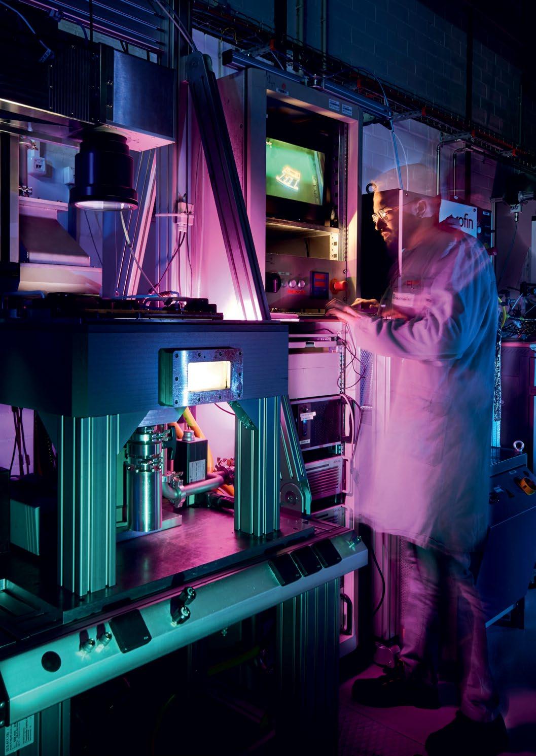

© Fraunhofer ILT, Volker Lannert, Aachen DDMC 2025 | Berlin | March 12-13, 2025 Call for Papers Range of Topics � Product Development � Technologies � Materials � Quality � Post Processing � Algorithms and Software � Sustainability and Circularity � Industrialization and Smart Production � Latest Industrial Trends and Success Stories Abstract Submission Deadline May 31, 2024

5 6
JUNE 2024
NEC, Birmingham, UK
The UK’s DEFINITIVE and most INFLUENTIAL
3D printing and additive manufacturing event.
Evaluate. Adopt. Optimise.
Analyse the opportunity
Discover your application
Learn from user success stories
Understand capabilities and limitations
Choose the right solution
Optimise existing technology
Consider enterprise adoption
Ensure return on investment
With more than 100 speakers and 200 exhibitors, discover your additive strategy at TCT 3Sixty.


www.tct3sixty.com
Register Now!
SCAN ME
AM for medical implants: An analysis of the impact of powder reuse in Powder Bed Fusion
The growing use of titanium Additive Manufacturing for the production of medical implants is a major success story for the industry. With this growth, however, come vast volumes of process data which need to be monitored to ensure compliance with tight regulatory requirements. Here, Peter Lindecke, amsight GmbH, explains how holistic analysis software can be used to monitor the impact of powder reuse strategies in Electron Beam Powder Fusion to ensure the best possible outcomes.
The field of Additive Manufacturing as a whole has witnessed significant growth in medical applications, with Powder Bed Fusion processes – which can be divided into Electron Beam Powder Bed Fusion (PBF-EB) and Laser Beam Powder Bed Fusion (PBF-LB) – taking the lead. These technologies offer the precision, efficiency, and ability to create complex structures.
As AM grows in tightly regulated industries such as medical, titanium is seeing wider use, as its biocompatibility, strength, and corrosion resistance make it ideal for implants and surgical devices. Titanium is now extensively used in medical applications which come into contact with human tissue, such as orthopaedic implants (hip and knee replacements), as well as craniofacial/ maxillofacial and dental implants, where its corrosion resistance and ability to bond to bone shine. Its strength and lightness is advantageous in prosthetics and orthotics. Beyond that, titanium's strength and durability make it ideal for surgical instruments.
The medical industry's stringent quality standards for implants and devices, however, necessitate that recycled titanium powder undergoes strict treatment. Whilst, in theory, it’s relatively simple to re-use powder in AM, these high industry standards
mean that batches of used powder might be disposed of because of a lack of familiarity with powder recycling requirements. There is, therefore, a need to improve the understanding and management of powder reuse. This includes under -
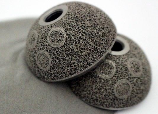
Metal Additive Manufacturing | Spring 2024 185 Vol. 10 No. 1 © 2024 Inovar Communications Ltd | contents | news | events | advertisers | website | newsletter | GETPDF Powder reuse impact analysis
Fig. 1 AM acetabular cups produced by implantcast GmbH (Courtesy implantcast GmbH)
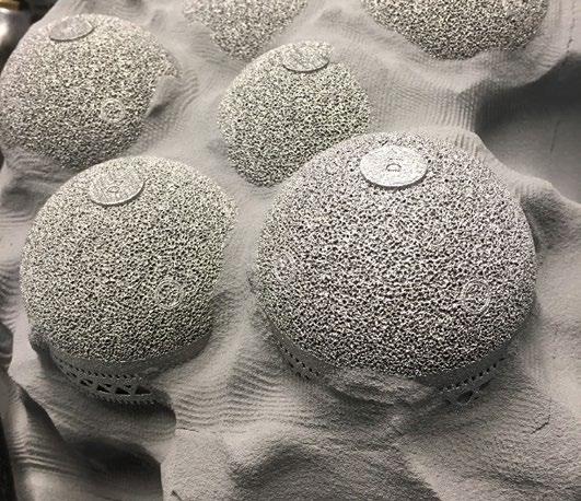
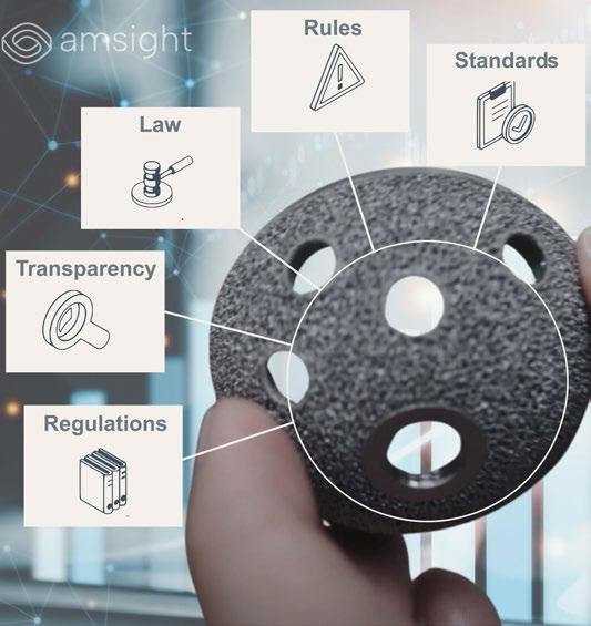
standing how ageing affects powder batches, and how to implement effective traceability measures to maintain (or even enhance) the material properties required for medical applications.
As titanium is also an expensive material, its waste in manufacturing processes can significantly increase product costs. Reusing titanium powder in AM parts production allows for the conservation of resources and reduces overall costs in the production of medical devices.
When considering sustainability, the production of titanium powder is energy-intensive and has a significant environmental impact. By reusing the powder, the need for powder production and disposal diminishes, reducing the carbon footprint associated with its manufacturing. Reusing titanium powder in Additive Manufacturing, therefore, plays a crucial role not only in sustainability but also in cost effectiveness. With the increasing need for superior, tailor-made medical implants and devices, the reuse of titanium powder when appropriate is increasingly vital.
Holistic quality and data management in regulated industries
When using Additive Manufacturing in the medical sector, the quality of the end product is intrinsically linked to the properties of the raw materials used. To ensure the best quality product, comprehensive data collection on powder ageing and composition – in tandem with consistent monitoring of the processes and the quality of the manufactured medical components – is essential. A holistic approach ensures that the implants and other medical devices produced meet the stringent standards required for medical applications (Fig. 3).
The meticulous study of powder ageing and composition emerges as a pivotal factor in ensuring the highest standards of material performance and sustainability. The
Metal Additive Manufacturing | Spring 2024 186 © 2024 Inovar Communications Ltd Vol. 10 No. 1 | contents | news | events | advertisers | website | newsletter | Powder reuse impact analysis
Fig. 2 Additively manufactured (PBF-EB) hip implants from implantcast GmbH shown in a powder 'cake' after the PBF-EB build process. The non-molten powder is blasted off in a Powder Recovery Station and fed back into the process through a special process (Courtesy implantcast GmbH)
Fig. 3 The requirements of Additive Manufacturing in regulated markets are numerous, so holistic data collection and analysis are becoming increasingly important (Courtesy amsight GmbH)
importance of data to the study of powder ageing and composition underlines this critical aspect by focusing on three key areas:
1. How, over time, the characteristics of metal powders can change due to exposure to the AM process and environmental factors. Detailed data on how these properties evolve is crucial to maintaining the integrity of the AM process and the quality of the final product.
2. Developing an understanding of the ageing process of powders allows for the implementation of predictive measures. This can prevent the use of degraded material that might compromise the structural and biological compatibility of medical components.
3. Thoroughly analysing powder composition and ageing, allowing manufacturers to make informed decisions on the recyclability of powders, thereby optimising resource usage and reducing waste without compromising quality.
Enhancing medical device manufacturing through advanced data management and quality control
In the highly regulated medical device manufacturing industry, comprehensive data collection is essential for compliance with quality standards and certification requirements, such as those of the FDA in the US, or for obtaining the CE mark indicating safety compliance within the EU. To ensure that medical components are safe and effective for intended use, it is essential to implement advanced data management systems (Fig. 4). These systems are designed to closely track and analyse every detail of the manufacturing process to facilitate compliance with industry regulations and ensure reliable device production.
ASTM F 3456:2022
Standard guideforpowderreuseschemain PowderBedFusionprocessesformedical applicationsfor Additive Manufacturing feedstockmaterials.
ISO/ASTM 52907:2019
Providestechnicalspecificationsfor metallic powders, includingdocumentation, sampling, and storage, but doesnot focus onsafetyaspects.
ISO/ASTM52904:2019
Focuseson processcharacteristicsand performanceinAdditiveManufacturing, particularlyfor theMetal Powder BedFusion processfor criticalapplications.
ISO/ASTMDTR52913-1
Technical reportin development, focuseson flowabilityparametersofpowders.
ISO/ASTM A FDIS 52928
Standard in progress, addressing the lifecycle management of metal powder feedstock, including testing methods and quality assurance.
Comprehensive data analysis on powder ageing and composition, combined with strict quality monitoring of medical components, is crucial in medical AM. As AM technologies advance, such a holistic strategy is key to driving innovation and ensuring the highest levels of patient safety and care.
Powder mixing strategies
Key powder characteristics include chemical composition, particle size distribution, particle morphology or flowability and packing behaviour, which can be highly influenced by the applied re-use strategies or storage condi -
“In the highly regulated medical device manufacturing industry, comprehensive data collection is essential for compliance with quality standards and certification requirements...”
Metal Additive Manufacturing | Spring 2024 187 Vol. 10 No. 1 © 2024 Inovar Communications Ltd | contents | news | events | advertisers | website | newsletter | GETPDF Powder reuse impact analysis
Fig. 4 Selection of relevant standards and standardisation activities relating to AM medical applications (Courtesy amsight GmbH)
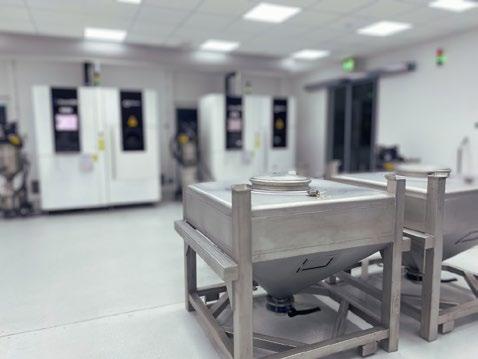
tions and thus lead to changes in manufacturing and part quality.
In Powder Bed Fusion, there are several strategies for handling and mixing metal powders, each impacting the quality and properties of the final products in different ways. The most common are shown in Fig. 5 and described in a simplified form as follows:
The batch methods
The Single Batch Method, where the same powder batch is reused until depleted with sieving between runs. There is also a Collective Ageing Method, which mixes batches of the same-aged powder for larger-scale use.
The top-up method
Batch method
Batch Method
Top-up method Refreshing method
The top-up method involves adding sieved or virgin powder to the remaining supply to maintain the required level, resulting in a stacked powder bed.
The refreshing method
Top - Up Method Refreshing Method
This method replaces material lost in the build and sieving processes with virgin powder, mixing the two to create a homogeneous mix.
The method chosen can significantly influence the mechanical properties, surface quality, and integrity of manufactured parts, with the selection depending on the final product's specific requirements and standards.
“Handling these data is challenging and, due to a lack of more appropriate tools, they are often managed through Microsoft Excel. However, this method is not only time-consuming but prone to errors, which may lead to inaccuracies down the line...”
Implementing an effective quality and data management system
AM part producers are inundated with vast amounts of heterogeneous data. Handling these data is challenging and, due to a lack of more appropriate tools, they are often managed through Microsoft Excel. However, this method is not only time-consuming but prone to errors, which may lead to inaccuracies down the line, false interpretations or delays in production. The lack of standardised data formats further complicates data analysis and utilisation.
With its data management software, amsight GmbH offers a comprehensive solution that addresses these challenges. The software automates data collection from various sources such as AM machines and peripheral equipment in order to streamline data management. Its robust platform supports easy data storage, search, and analysis, and is equipped with advanced tools for deep data understanding and trend identification.
The amsight software increases efficiency by reducing manual data entry and speeds up the Additive Manufacturing evaluation
Metal Additive Manufacturing | Spring 2024 188 © 2024 Inovar Communications Ltd Vol. 10 No. 1 | contents | news | events | advertisers | website | newsletter |
Fig. 5 Powder containers in the series production of implants at implantcast GmbH (left); graphic representation of the three common powder mixing strategies (right) (Courtesy amsight GmbH)
Powder reuse impact analysis
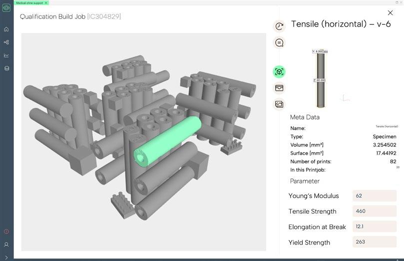
process. Its analytical capabilities aid in making informed decisions, thereby streamlining processes in both production and R&D. This leads to improved efficiency and innovation in material and process development.
Case study: serial production of Ti-6Al-4V PBF-EB hip implants
To assess the impact of powder management on mechanical properties in the serial production of medical devices using Ti-6Al-4V, three Arcam Q10 Plus PBF-EB machines were used to produce a qualification build job sixteen times over three months (Fig. 6). The powder handling strategy involved the refreshing method, which mixes new powder with used powder to maintain consistency. Before each production cycle, the powder was characterised using various tech -
“The amsight software increases efficiency by reducing manual data entry and speeds up the AM evaluation process. Its analytical capabilities aid in making informed decisions, thereby streamlining processes in both production and R&D.”
niques, including flow analysis, sieve analysis, dynamic image analysis, laser diffraction, and gas analysis. The quality of the test specimens was then evaluated for fatigue strength, tensile strength, elongation at break, hardness, and roughness.
All data were recorded and evaluated using the holistic data management software from amsight
(Fig. 7). This allowed an easy evaluation of correlations between different influencing variables. The data was largely provided by implantcast GmbH and the Fraunhofer IAPT; the collaboration was made possible by the PERU (GAN: 03LB5007) project, funded by the German Federal Ministry for Economic Affairs and Climate Protection BMWK.
Metal Additive Manufacturing | Spring 2024 189 Vol. 10 No. 1 © 2024 Inovar Communications Ltd | contents | news | events | advertisers | website | newsletter | GETPDF
Fig. 6 Qualification build job in a 3D view in amsight software. All relevant data can be seen with just one click (Courtesy amsight GmbH)
Powder reuse impact analysis
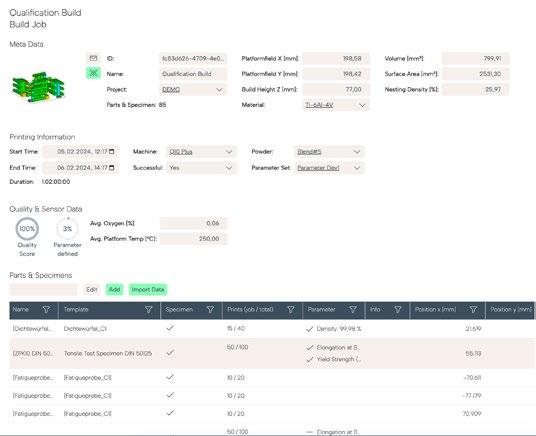
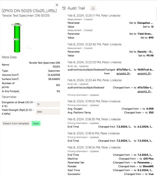
Key findings
The exploration of the Additive Manufacturing data indicates that virgin titanium powder displays lower yield strength compared to powder that has undergone ageing (Fig. 8); an increase in the yield strength can be observed from the fourth cycle onwards. This effect can also be observed in the fatigue strength tests. However, this increase is associated with a limitation that particularly affects the ductility of the material.
As shown in Fig. 9, an inverse relationship between oxygen content and ductility in titanium raises concerns about material embrittlement. As oxygen content increases from 590 ppm to 830 ppm, the material exhibits increased tensile strength as well as increased variability in elongation. This embrittlement can push the material's properties to – or even beyond – acceptable lower limits, which is particularly troubling for critical applications where material failure could have dire consequences.
Fig. 10 shows that as the powder used in Additive Manufacturing ages, its oxygen concentration increases. This ageing effect is evidenced by the consistent rise in oxygen levels across successive build cycles when employing the refreshing method. The point of oxygen saturation within the powder varies based on a range of factors, including the ratio of new to used powder and the specific process parameters involved in manufacturing. Due to these variables, it is imperative to continuously monitor the oxygen content within the powder. This ensures that the mechanical integrity of the additively manufactured components is maintained and prevents the onset of material properties degradation.
The regularly tested refreshed powder shows that the sphericity of the powder increases with increasing use (Fig. 8). Fig 11 shows the flow rate of powder used over various build cycles. There is a decrease in the time it takes for 50 g of powder to flow, indicating that the powder becomes more flowable as it is reused.
Metal Additive Manufacturing | Spring 2024 190 © 2024 Inovar Communications Ltd Vol. 10 No. 1 | contents | news | events | advertisers | website | newsletter |
Fig. 7 Display from the amsight software: all production data from powder to heat treatment is accessible via a user-friendly interface. The data are stored in a tamper-proof and standardised manner. Analyses are preset and accessible for selected employees (Courtesy amsight GmbH)
Powder reuse impact analysis
Powder reuse impact analysis
820
820
Machine A
Machine B Machine C
C Printer A
Buildcycle0 –15 (Refreshing Method )
Build cycle 0-15 (refreshing method)
The dotted horizontal line labelled 'SPHT3 Mean' represents the sphericity of the refreshed powder, measured by the Shape Characteristic Index (Courtesy amsight GmbH)
This increase in flowability correlates with the findings shown in Fig 8, which demonstrates that the powder's sphericity improves with each reuse cycle. As the powder particles become rounder, they can move past each other more easily, which can enhance the flow rate. Improved flowability is significant for the Additive Manufacturing process because it facilitates a smoother, more consistent spreading process. This reduces the likelihood of errors in the fresh powder, thereby requiring fewer corrections.
This improved flowability translates into tangible time savings. A more flowable powder can reduce the total time of the qualification build job by up to forty minutes in an average total production time of
Metal Additive Manufacturing | Spring 2024 191 Vol. 10 No. 1 © 2024 Inovar Communications Ltd | contents | news | events | advertisers | website | newsletter | GETPDF
Fig. 9 Scatterplot of elongation at break, tensile strength, and oxygen concentration of the horizontally built specimen (Courtesy amsight GmbH)
Fig. 8 Data of three different AM machines over 16 powder ageing cycles. The error bars show the degree of variation in the yield strength (Ti-6Al-4V) for each AM machine.
850
Printer
SPHT3
Shape Characteristic Index 0,95 0,92 Elongation at break [%] 910 14 Tensile Strenght [N/mm²] 930 945 Oxygen content [ppm]
830 10 Lower Limit Yield strength [MPa] Shape characteristic index
Yieldstrength[Mpa]
Printer B
Mean
590
0.92
0.95
850
Fig. 10 Oxygen content of the individual aged powder batch from cycle 0 to 15 (Courtesy amsight GmbH)
Oxygen content [ppm] 1000 Build cycle (Refreshing Method) 400 700 1 7 15 4 11 Flow rate [s/50g] 27 Build cycle (Refreshing Method) 24,5 26 1 7 15 5 11 Oxygen content [ppm] Flow rate [s/50g] Build cycle (refreshing method) Build cycle (refreshing method) 1000 27 700 26 400 1 1 5 7 11 15 4 7 11 15 24.5
Fig. 11 Flowability of titanium powder across several build cycles (Courtesy amsight GmbH)
“Powder ageing improves some properties, but also impairs others –in particular, the increase in oxygen content in the powder can lead to embrittlement and must, therefore, be tracked precisely.”
twenty-eight hours. This resulted from the evaluation of the build log files. Such an efficiency gain is substantial when considering the scale of manufacturing operations and the potential for these time savings to accumulate over multiple production cycles. Therefore, the observed enhancement in powder flowability due to increased sphericity contributes to significant time and cost efficiencies.
Another finding is the variation in quality between AM machines. The
boxplot graph in Fig. 8 illustrates variations in the performance of different PBF-EB machines, specifically machine A, which shows a larger standard deviation in the produced components. There seems to be a plausible correlation between the ‘time to vacuum’ (time until the system has created a vacuum to start the process) and the performance deviations, which may be attributable to leaks within the machine. It becomes clear that such complex issues in the Additive Manufacturing
process can only be detected through persistent and holistic data analysis.
The results show that the Additive Manufacturing process for titanium has a resource-efficient behaviour, especially in connection with the reuse of powder. Powder ageing improves some properties, but also impairs others – in particular, the increase in oxygen content in the powder can lead to embrittlement and must, therefore, be tracked precisely. It is crucial to subject the production process to continuous monitoring of influencing factors and trends through a holistic data management and analysis software in order to detect machine and process errors at an early stage.
Author Peter Lindecke Co-Founder & CCO amsight GmbH
Hamburg Germany peter.lindecke@amsight.de www.amsight.de
Metal Additive Manufacturing | Spring 2024 192 © 2024 Inovar Communications Ltd Vol. 10 No. 1 | contents | news | events | advertisers | website | newsletter |
Powder reuse impact analysis


Industry events
Metal AM magazine is dedicated to driving awareness and development of metal Additive Manufacturing and its related technologies. Key to this aim is our support of a range of international partner conferences and exhibitions. View our complete events listing on www.metal-am.com
2024
America Makes TRX
April 9–11, Golden, CO, United States www.americamakes.us/events/trx-spring/
MACH 2024
April 15–19, Birmingham, United Kingdom www.machexhibition.com
Hannover Messe
April 22–26, Hannover, Germany www.hannovermesse.de
ImplementAM – Atlanta
April 24, Atlanta, GA, United States www.4spe.org/i4a/pages/index.cfm?pageid=8475
AMC 2024
April 25–27, Antalya, Turkey www.amctr.org
CDFAM Symposium
May 7–8, Berlin, Germany www.cdfam.com
Additive Manufacturing Coalition DC Fly-In
May 8–10, Washington, D.C., United States www.addmfgcoalition.org/dc-fly-in
Space Tech Expo US
May 14–15, Long Beach, CA, United States www.spacetechexpo.com
Rapid.Tech 3D
May 14–16, Erfurt Germany www.rapidtech-3d.com
If you would like to see your metal Additive Manufacturing related event listed in this magazine and on our websites, please contact:
Merryl Le Roux, Operations and Partnerships Manager merryl@inovar-communications.com
The Advanced Ceramics Show
May 15–16, Birmingham, United Kingdom www.advancedceramicsshow.com
The Advanced Materials Show
May 15–16, Birmingham, United Kingdom www.advancedmaterialsshow.com
The National Manufacturing & Supply Chain Conference & Exhibition
May 28–29, Dublin, Ireland www.manufacturingevent.com
ADDIT3D
June 3–7, Bilbao, Spain addit3d.bilbaoexhibitioncentre.com
3D Print Lyon
June 4–6, Lyon, France www.3dprint-exhibition-lyon.com
EPMA AM Seminar
June 4–5, Augsburg, Germany seminars.epma.com/event/am-seminar-2024/
Smart Manufacturing Experience
June 4–5, Pittsburgh, PA, United States www.smartmanufacturingexperience.com
TCT 3Sixty
June 5–6, Birmingham, UK www.tct3sixty.com
Advanced Manufacturing for Defense
June 11–12, Pasadena, CA, United States www.idga.org/events-advancedmanufacturing
FABTECH Canada 2024
June 11–13, Toronto, Canada canada.fabtechexpo.com
EPHJ
June 11–14, Geneva, Switzerland www.ephj.ch
PowderMet2024 / AMPM2024
June 16–19, Pittsburgh, PA, USA www.powdermet2024.org | www.ampm2024.org
Metal Additive Manufacturing | Spring 2024 194 © 2024 Inovar Communications Ltd Vol. 10 No. 1 | contents | news | events | advertisers | website | newsletter | Events guide
Running an event? Partner with us
Rapid + TCT
June 25–27, Los Angeles, CA, USA www.rapid3devent.com
WBE 2024
August 8–10, Guangzhou, China en.battery-expo.com
PMTi 2024
September 4–6, Madrid, Spain www.pmti2024.com
IMTS 2024
September 9–14, Chicago, IL, USA www.imts.com
RM Forum
September 25–26, Milan, Italy www.rmforum.it
EURO PM2024
September 29– October 2, Malmö, Sweden www.europm2024.com
The Advanced Materials Show USA
October 8–9, Pittsburgh, PA, United States www.advancedmaterialsshowusa.com
World PM2024
October 13–17, Yokohama, Japan www.worldpm2024.com
Scotland Manufacturing & Supply Chain Conference & Exhibition
October 23–24, Glasgow, Scotland www.manufacturingexposcotland.com
Formnext
November 19–22, Frankfurt, Germany www.formnext.com
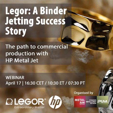
Over just one hour, discover how Legor Jewellery has embraced innovation, leveraging HP 3D Metal Jet technology to revolutionise its production process. Explore firsthand how Additive Manufacturing breaks free from traditional constraints, offering unparalleled design flexibility and efficiency. Through captivating examples and expert insights, witness how this technology transforms workflow and ignites creativity.
This webinar isn’t just about showcasing cutting-edge technology; it’s about sparking a mindset shift.
Join us for an eye-opening webinar where HP teams up with Legor Jewellery to hear about their “Beyond Extraordinary” workshop, which challenges norms and explores the gamechanging potential of 3D printing in jewellery manufacturing and beyond.
This is an innovative journey into the expansive possibilities offered by HP Metal Jet 3D printing technology across various industries, not just limited to jewellery.
AM China 2025
March 10–12, Shanghai, China www.amatex.cn
Fraunhofer DDMC 2025
March 12–13, Berlin, Germany www.ddmc-fraunhofer.de
AMUG 2025
March 30–April 3, Chicago, IL, USA www.amug.com
The initiative encourages a shift from conventional design approaches, enabling a comprehensive exploration of Additive Manufacturing’s potential in product development and design. The focus aims to catalyse innovation across sectors such as automotive, aerospace, and industrial design.




Metal Additive Manufacturing | Spring 2024 195 Vol. 10 No. 1 © 2024 Inovar Communications Ltd | contents | news | events | advertisers | website | newsletter | GETPDF Events guide
2025









WORLD. LEADING. INDUSTRYSHOW. HANNOVER MESSE 2024 ENERGIZING A SUSTAINABLE INDUSTRY Products and solutions at #HM24 22 – 26 April 2024 Hannover, Germany hannovermesse.com
Advertisers’ index & buyer’s guide
Our advertisers’ index and buyer’s guide serves as a convenient guide to suppliers of AM machines, materials, part manufacturing services, software and associated production equipment. In the digital edition of Metal AM magazine, available at www.metal-am.com, simply click on a company name to view its advert, or on the weblink to go directly to its website.
Metal Additive Manufacturing | Spring 2024 197 Vol. 10 No. 1 © 2024 Inovar Communications Ltd | contents | news | events | advertisers | website | newsletter | GETPDF
Advertisers’ index / buyer’s guide
Additive Industries 06 www.additiveindustries.com AML3D Limited 15 www. aml3d.com Avimetal AM Tech Co., Ltd 115 www.avimetalam.com BLT - Bright Laser Technologies 55 www.xa-blt.com Eplus3D 75 www.eplus3d.com Ermaksan Additive 47 www.ermaksan.com.tr Farsoon Technologies 53 www.farsoon.com Guangdong Hanbang 3D Tech Co., Ltd. 77 en.hb3dp.com TRUMPF SE + Co. KG 35 www.trumpf.com Laser Beam Powder Bed Fusion (PBF-LB) AM MACHINES JEOL Ltd. 59 www.jeol.co.jp Xi’an Sailong AM Technologies Co. Ltd 122 www.slmetal.com Wayland Additive Limited 19 www.waylandadditive.com Electron Beam Powder Bed Fusion (PBF-EB) Binder Jetting (BJT) Desktop Metal, Inc. OBC www.desktopmetal.com MetShape GmbH 48 www.metshape.com Hybrid AM Matsuura Machinery Ltd 111 www.matsuura.de Directed Energy Deposition (DED) BLT - Bright Laser Technologies 55 www.xa-blt.com Hybrid Manufacturing Technologies 40 www.hybridmanutech.com MetalWorm AM Technologies Inc 43 www.metalworm.com Nikon Corporation 27 www.nikon.com TRUMPF SE + Co. KG 35 www.trumpf.com Material Jetting (MJT) Vat Photopolymerisation (VPP) SPEE3D 04 www.spee3d.com Cold Spray GROB-WERKE GmbH & Co. KG 32 www.grobgroup.com Lithoz GmbH 68 www.lithoz.com
Metal Additive Manufacturing | Spring 2024 198 © 2024 Inovar Communications Ltd Vol. 10 No. 1 | contents | news | events | advertisers | website | newsletter | Advertisers’ index / buyer’s guide Addiblast by FerroECOBlast 86 www.addiblast.com AM Solutions - Rösler Group 95 www.solutions-for-am.com EDM Network Inc. 103 www.edmnetwork.com EDM Performance Accessories, Inc. 105 edmperformance.com Indium Corporation® 92 www.indium.com Inert Corporation 79 www.inertcorp.com joke Technology GmbH 125 www.joke-technology.com Solukon Maschinenbau GmbH 37 www.solukon.de TOP Environmental Technology 113 www.iectop.com Volkmann GmbH 46 www.volkmann.info
AUTOMATION Alphabetical index 3D Print Lyon 176 Addiblast by FerroECOBlast 86 Additive Industries 06 AM China 2025 193 AM Solutions - Rösler Group 95 America Makes 175 American Isostatic Presses 119 AML3D Limited 15 AMUG 2025 166 Applied Optimization, Inc. 64 Arcast Inc. 90 /112 ATM Qness GmbH 87 ATO by 3D Lab 36 Avimetal AM Tech Co., Ltd 115 BLT - Bright Laser Technologies 55 Blue Power Casting Systems GmbH 67 Burloak Technologies 84 Carbolite Gero Ltd. 57 Carpenter Additive 56 Centorr Vacuum Industries 61 Chung Yo Materials 88 CM Furnaces Inc. 30 CNPC Powder Group Co., Ltd. 23 Constellium 51 Daido Steel Co., Ltd. 81 Desktop Metal, Inc. OBC DNA AM 24 DSH Technologies 97 ECM Technologies S.A.S. 69 EDM Network Inc. 103 EDM Performance Accessories, Inc. 105 Elnik Systems 08 Eltra GmbH 123 Eplus3D 75 Epson Atmix Corporation 33 Equispheres 21 Ermaksan Additive 47 Euro PM2024 IBC Farsoon Technologies 53 Fraunhofer DDMC 2025 183 Formnext 126 Granutools 54 GROB-WERKE GmbH & Co. KG 32 Guangdong Hanbang 3D Tech Co., Ltd. 77 Hannover Messe 196 Hiperbaric 50 Höganäs AB 28 Hybrid Manufacturing Technologies 40 i3DMFG™ 74 IMR Metal Powder Technologies GmbH 38 IN3DTEC © 106 Indium Corporation® 92 more >>> HIP SYSTEMS & SERVICES American Isostatic Presses 119 www.aiphip.com Hiperbaric 50 www.hiperbaric.com Isostatic Toll Services 119 www.isostatictollservices.com Pressure Technology, Inc. 73 www.pressuretechnology.com Quintus Technologies AB 63 www.quintustechnologies.com For information on advertising contact: Jon Craxford Advertising Sales Director Tel: +44 207 1939 749 jon@inovar-communications.com Wish you were listed?
PRE & POST-PROCESSING TECHNOLOGY, PROCESS
HEAT TREATMENT &
Metal Additive Manufacturing | Spring 2024 199 Vol. 10 No. 1 © 2024 Inovar Communications Ltd | contents | news | events | advertisers | website | newsletter | GETPDF Advertisers’ index / buyer’s guide Indo-MIM 99 /101 Inert Corporation 79 Ipsen Global 117 Isostatic Toll Services 119 JEOL Ltd. 59 Jiangsu Tiangong Technology Co., Ltd - TGTi 71 Jiangxi Yuean Superfine Metal Co., Ltd. 121 joke Technology GmbH 125 Kennametal Inc. 52 Kymera International 65 LECO Corporation 102 Linde Advanced Material Technologies Inc. IFC Lithoz GmbH 68 LÖMI GmbH 98 Lucideon 49 Matsuura Machinery Ltd 111 Metalpine GmbH 29 /31 MetalWorm AM Technologies Inc. 43 MetShape GmbH 48 Microtrac Retsch GmbH 83 Mimete S.r.l. 16 MUT Advanced Heating GmbH 66 NEL Hydrogen AS 108 Nikon Corporation 27 Oqton, Inc. 17 Osaka Titanium Technologies Co. Ltd. 91 PowderMet2024 / AMPM2024 165 Pressure Technology, Inc. 73 Proterial, Ltd. 89 PureAire Monitoring System, Inc. 41 Quintus Technologies AB 63 RAPID + TCT 2024 140 Rio Tinto 42 S&S Scheftner GmbH 20 Sandvik Additive Manufacturing 10 Solukon Maschinenbau GmbH 37 Space Tech Expo US 2024 154 SPEE3D 04 T-M Vacuum Products Inc 76 TANIOBIS GmbH 45 TAV Vacuum Furnaces SPA 39 TCT 3Sixty 2024 184 Tekna 13 toolcraft AG 70 TOP Environmental Technology 113 TRUMPF SE + Co. KG 35 Ultra Fine Specialty Products 25 VBN Components AB 60 VDM Metals 109 voestalpine AG 93 Volkmann GmbH 46 Wayland Additive Limited 19 World PM2024 200 Xi’an Sailong AM Technologies Co. Ltd 122 Zenith Tecnica 82
SINTERING Carbolite Gero Ltd. 57 www.carbolite-gero.com Centorr Vacuum Industries 61 www.vacuum-furnaces.com CM Furnaces Inc. 30 www.cmfurnaces.com ECM Technologies S.A.S. 69 www.ecm-furnaces.com Elnik Systems 08 www.elnik.com Ipsen Global 117 www.ipsenglobal.com LÖMI GmbH 98 www.loemi.com MUT Advanced Heating GmbH 66 www.mut-jena.de T-M Vacuum Products Inc 76 www.tmvacuum.com TAV Vacuum Furnaces SPA 39 www.tav-vacuumfurnaces.com Sintering, debinding and heat treatment systems DSH Technologies 97 www.dshtech.com Toll debinding & sintering NEL Hydrogen 108 www.nelhydrogen.com PureAire Monitoring System, Inc. 41 www.pureairemonitoring.com Gas, gas generation & gas measurement Applied Optimization, Inc. 64 www.appliedo.com DNA AM 24 www.dna.am Oqton, Inc. 17 www.oqton.com AM SOFTWARE

Metal Additive Manufacturing | Spring 2024 201 Vol. 10 No. 1 © 2024 Inovar Communications Ltd | contents | news | events | advertisers | website | newsletter | GETPDF Advertisers’ index / buyer’s guide METAL POWDER & WIRE POWDER PRODUCTION & ANALYSIS Arcast Inc 112 www.arcastmaterials.com Avimetal AM Tech Co., Ltd 115 www.avimetalam.com BLT - Bright Laser Technologies 55 www.xa-blt.com Carpenter Additive 56 www.carpenteradditive.com Chung Yo Materials 88 www.cymaterials.com.tw CNPC Powder Group Co., Ltd. 23 www.cnpcpowder.com Constellium 51 www.constellium.com Daido Steel Co., Ltd. 81 www.daido.co.jp Epson Atmix Corporation 33 www.atmix.co.jp Equispheres 21 www.equispheres.com Höganäs AB 28 www.hoganas.com IMR Metal Powder Technologies 38 www.imr-metalle.com Indo-MIM 99 www.indo-mim.com Jiangxi Yuean Advanced Mat. Co., Ltd 121 www.yueanmetal.com Kennametal Inc. 52 www.kennametal.com Metal powders Kymera International 65 www.kymerainternational.com Linde Advanced Material Tech. Inc. IFC www.linde-amt.com Metalpine GmbH 29 /31 www.metalpine.at Mimete S.r.l. 16 www.mimete.com Osaka Titanium Technologies Co. Ltd. 91 www.osaka-ti.co.jp Proterial, Ltd. 89 www.proterial.com Rio Tinto 42 www.riotinto.com S&S Scheftner GmbH 20 www.scheftner.dental Sandvik Additive Manufacturing 10 www.additive.sandvik TANIOBIS GmbH 45 www.taniobis.com Tekna 13 www.tekna.com Ultra Fine Specialty Products 25 www.ultrafinepowder.com VDM Metals 109 www.vdm-metals.com Arcast Inc. 90 www.arcastinc.com ATO by 3D Lab 36 www.3d-lab.pl Blue Power Casting Systems GmbH 67 www.bluepower-casting.com Tekna 13 www.tekna.com Jiangsu Tiangong Technology Co., Ltd 71 www.tiangongti.com Atomisers Wire Powder processing, classification & analysis ATM Qness GmbH 87 www.qatm.com Blue Power Casting Systems GmbH 67 www.bluepower-casting.com Eltra GmbH 123 www.eltra.com Granutools 54 www.granutools.com LECO Corporation 102 www.leco.com Microtrac Retsch GmbH 83 www.microtrac.com
PART MANUFACTURERS
Metal Additive Manufacturing | Spring 2024 202 © 2024 Inovar Communications Ltd Vol. 10 No. 1 | contents | news | events | advertisers | website | newsletter | Advertisers’ index / buyer’s guide 3D Print Lyon 176 www.3dprint-exhibition-lyon.com AM China 2025 193 www.amatex.cn AMUG 2025 166 www.amug.com Euro PM2024 IBC www.europm2024.com Fraunhofer DDMC 2025 183 www.ddmc-fraunhofer.de Formnext 126 www.formnext.com Hannover Messe 196 www.hannovermesse.de PowderMet2024 / AMPM2024 165 www.powdermet2024.org / www.ampm2024.org RAPID + TCT 2024 140 www.rapid3devent.com Space Tech Expo US 2024 154 www.spacetechexpo.com TCT 3Sixty 2024 184 www.tct3sixty.com World PM2024 200 www.worldpm2024.com EVENTS & COURSES America Makes 175 www.americamakes.us DSH Technologies 97 www.dshtech.com Lucideon 49 www.lucideon.com CONSULTING, TRAINING, MARKET DATA & ASSOCIATIONS
AM Solutions - Rösler Group 95 www.solutions-for-am.com BLT - Bright Laser Technologies 55 www.xa-blt.com Burloak Technologies Inc. 84 www.burloaktech.com Hybrid Manufacturing Technologies 40 www.hybridmanutech.com i3DMFG™ 74 www.i3dmfg.com IN3DTEC © 106 www.in3dtec.com Indo-MIM 101 www.indo-mim.com Kennametal Inc. 52 www.kennametal.com Sandvik Additive Manufacturing 10 www.additive.sandvik toolcraft AG 70 www.toolcraft.de VBN Components AB 60 www.vbncomponents.com voestalpine AG 93 www.voestalpine.com Xi’an Sailong AM Technologies Co. Ltd 122 www.slmetal.com Zenith Tecnica 82 www.zenithtecnica.com Access all our back issues at www.metal-am.com
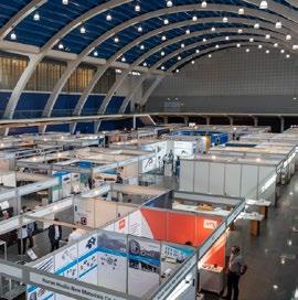



RESERVE YOUR EXHIBITION STAND 29 September - 2 October 2024, Malmö THE ONLY EVENT IN COVERING ALL ASPECTS OF POWDER METALLURGY EUROPE • Explore cutting-edge products and services in one of the birthplace of PM. • Gain insights into the latest advancements in Powder Metallurgy and related fields. • Meet Experts in Powder Production & Characterisation, Binder Jetting, Beam Based AM, Sinter Based AM, Consolidation • Engage with technical presentations attracting industry professionals from across Europe. • Full Supply Chain Representation: From materials to applications • Network with current customers and potential collaborators. europm2024.com STAFF ENTRANCES FREE INVITATIONS FOR YOUR CLIENTS TICKETS FOR TECHNICAL SESSIONS AND MANY MORE ADVANTAGES
We have solutions for your manufacturing challenges
Desktop Metal’s 3D printing solutions are trusted worldwide by the world’s biggest and smallest companies — to solve the toughest challenges and enable once-impossible innovations
Supply Chain Difficulties
Long Waits for Tooling
Delivering Product Faster
Complex Geometries
Affordable Solutions
Flexibility for Surprises
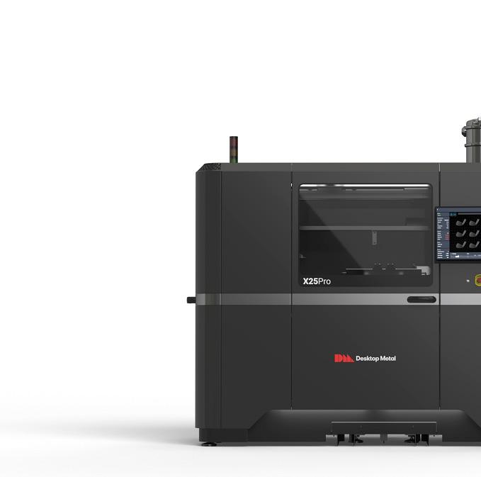
Our portfolio of metal printers offers 20+ metals, including ceramics
Our Additive Manufacturing 2.0 Production team members can help you get started today. Visit TeamDM.com/AMPro
GET STARTED
The Ultimate Guide to Laser-Free Metal 3D Printing
This 40-page guide is a comprehensive overview of metal binder jetting — the most promising ASTM-recognized 3D printing technology for the mass production of metal parts and products.
INSIDE:
• Learn the benefits of binder jetting technology, which requires no expensive lasers and prints at high speeds
• Explore how binder jetting is similar to long-trusted Metal Injection Molding (MIM) processes
• Review details on final part density and quality of binder jetted parts
• See the incredible flexibility for printing stainless steels, nickel-based alloys, and other metals, including aluminum, titanium, and copper
• Read about customers using Desktop Metal systems

Download the Guide at TeamDM.com/BinderJetGuide
