International Journal for Research in Applied Science & Engineering Technology (IJRASET) ISSN: 2321-9653; IC Value: 45.98; SJ Impact Factor: 7.538 Volume 10 Issue VI June 2022- Available at www.ijraset.com ARCHITECTURAL OVERVIEW
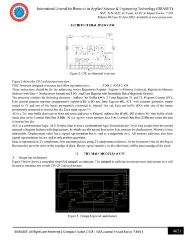
Figure 2. CPU architectural overview Figure 2 shows the CPU architectural overview. CISC Processor designed to execute the Following Instructions: 1. ADD 2. AND 3. OR These instructions should be for the addressing modes Register-to-Register, Register-to-Memory (Indirect), Register-to-Memory (Indirect with Base + Displacement format) and LBI (Load Base Register with Immediate Data (Magnitude format)). The processor contains the following elements - Address Out Buffer (AO), 2 Temp Registers T1 and T2, Program Counter (PC), Four general purpose registers (programmer's registers) R0 to R3 and Base Register (B), ALU with constant generator, output routed to T1 and one of the inputs permanently connected to Internal Bus (a), Data out buffer (DO) with one of the inputs permanently connected to internal bus (b), Data input register DI. AO is a Tri- state buffer that receives from and sends addresses to External Address Bus (EAB). DO is also a Tri- state buffer which sends data out to External Data Bus (EDB). DI is a register which receives data from External Data Bus (EDB) and writes the data to internal bus (b). ALU is a combinational logic. ALU B input select is also a combinational logic Instructions are 1-byte long except when the second operand is Register Indirect with displacement. In which case the second Instruction byte contains the displacement. Memory is byte addressable. Displacement value has a signed representation but is read as a magnitude only. All memory addresses also have signed representation but are read as only positive quantities. Data is represented in 2's complement form and manipulated using 2's complement arithmetic. In the Execution Unit, all the Reg to Bus transfers are to be done on the negedge of clock. Bus to register transfers, on the other hand, will be done posedge of the clock. II. THE MAIN MODULES of CPU A. Design top Architecture Figure 3 below shows a somewhat simplified datapath architecture. This datapath is sufficient to execute most instructions so it will be used to introduce the overall CPU IP Core architecture.
Figure 3. Design Top level Architecture
©IJRASET: All Rights are Reserved | SJ Impact Factor 7.538 | ISRA Journal Impact Factor 7.894 |
4621