
31 minute read
Industry Report

from 3d
by Hiba Dweib

Part 5 of 5 Designing with FPGAs: FPga-Embedded Processors
Sani theo & nidhi Kathuria
Advertisement
Varsha agrawal
FPGA devices are suitable for implementing parallel algorithms. However, sequential algorithms, especially those that do not demand large processing power, are easier to implement as a program in a microprocessor. Many applications require both microprocessor and an FPGA array. One possible way to implement this is to have separate CPU and FPGA chips. But the better approach is to combine them into a single chip. This reduces the power consumption, leads to simple board layout and fewer problems with signal integration and EMI.
This article gives information on FPGA-embedded processors with particular emphasis on the Embedded Development Kit (EDK) from Xilinx. The article also presents an illustrative example of a hands-on experience with the EDK design.
FPGA-embedded processors
There are two types of CPU cores for FPGAs, namely, hard and soft. Hard CPU core is a dedicated part of the integrated circuit, whereas a soft CPU is implemented utilising general-purpose FPGA logic cells.
Examples of FPGA chips with hard CPU cores include Virtex-4FX and Virtex-5 FXT series with PowerPC cores, and Atmel’s FPSLIC with an AVR core. Some of the soft CPU cores include MicroBlaze and PicoBlaze that are used for the FPGAs manufactured by Xilinx, and Nios II processors that are limited to Altera devices.
MicroBlaze has a proprietary 32bit RISC architecture and a soft CPU core designed by Xilinx for use in their FPGAs. PicoBlaze has a proprietary 8-bit RISC architecture and a CPU core
Fig. 1: Embedded-processor design process
Fig. 2: The path for project file
developed by Xilinx. Nios-II has a proprietary 32-bit RISC architecture and a processor core developed by Altera for use in their FPGAs. It comes in three variants, namely, Nios II/f, Nios II/s and Nios II/e.
The soft processor is typically described in a Hardware Description Language (HDL) or netlist. Unlike the hard processor, a soft processor must be synthesized and fitted into the FPGA fabric. In both hard as well as soft processor systems, the local memory, processor busses, internal peripherals, peripheral controllers and memory controllers must be built from the FPGA’s general-purpose logic.
Some of the advantages offered by an FPGA-embedded processor over a typical embedded processor include customisation, obsolescence mitigation, component and cost reduction and hardware acceleration. The embedded-processor-system designer has the complete flexibility to select any combination of peripherals and controllers. In addition, he can design new peripherals to meet any non-standard peripheral set requirement. As an example, if the designer wants six UARTs for his design, off-the shelf processor with six UARTs is not available. However, the same can be implemented in an FPGA easily.
Some of the disadvantages of FPGA-embedded processor include increased tool complexity and design methodology, which require more attention from the embedded designer. Moreover, unlike an off-the-shelf processor, the hardware platform for the FPGA-embedded processor must be designed. If a standard off-the-shelf processor can do the job, that processor will be less expensive in comparison with the FPGA capable of an equivalent processor design. However, if an FPGA is already used in the system, consuming unused gates or a hard processor in the FGPA will make the embedded-processor system’s cost inconsequential.

Fig. 3: Base System Builder

Fig. 4: Custom board selection
To facilitate FPGA-embedded processor design, FPGA manufacturers offer extensive libraries of intellectual property (IP) in the form of peripherals and memory controllers. Some of the peripherals and peripheral controllers provided include general-purpose I/O, UART, timer, debug, SPI, DMA controller, Ethernet and so on. Some of the memory controllers include SRAM, Flash, SDRAM and Compact Flash.
Embedded Development Kit (EDK)
Embedded Development Kit (EDK) is a suite of tools and intellectual property (IP) that allows you to design and implement a complete embedded processor system in a Xilinx FPGA device. The aim of the EDK is to simplify the embedded-processor design process as it provides an umbrella covering all things related to embedded processor and its design. It may be mentioned here that EDK is specific to the FPGAs from Xilinx.
The EDK comprises two main components, namely, the Xilinx Platform Studio (XPS) and the Software Development Kit (SDK). XPS is used primarily for embedded-processor hardware system development, including configuration of the microprocessor, peripherals and the interconnection of these components, along with their respective property assignments. XPS has a base system builder (BSB) wizard that quickly and efficiently establishes a working design. The wizard is generally used to create the foundation of a new embedded design project.
SDK is the recommended software development environment for writing the software code for the embedded processors. Fig. 1 shows the embedded-processor design process.
Creating an EDK project
This section discusses how to create an EDK-driven design task to blink eight LEDs on and off at a frequency of 50Hz.
The different steps for designing the blinking of the LEDs are: 1. Open XPS by selecting Start → Programs → Xilinx ISE Design Suite 13.4_1 → EDK → Xilinx Platform Studio 2. From the dialogue box, select Create New Project Using Base System Builder 3. A window will appear titled Create New XPS Project Using BSB Wizard asking you to specify the folder to place the project. Set the desired path. (We have selected C:\edk as shown in Fig. 2.) 4. Then select the interconnect type, either as processor local bus (PLB) or advanced extensible interface (AXI), depending on the FPGA series you are using. As mentioned in the wizard, PLB is a legacy bus standard used by Xilinx that supports current FPGA families, including Spartan 6 and Virtex 6. It will not support new FPGA families. AXI is an interface standard recently adopted by Xilinx as the standard interface used for all current and future versions of Xilinx IP and tool flows. Choose among the two depending upon the FPGA family you are using. We are doing the design using Virtex-5, so we have selected PLB system. Click OK button 5. In the next window select ‘I would like to create a new design’ option and click Next, as shown in Fig. 3 6. A window appears asking the designer to select the board. If you have a standard development board from Xilinx mentioned in the list, select the first option ‘I would like to create a system for the following development board’ and fill in the vendor name as Xilinx and your board name. Otherwise, select the second option ‘I would like to create a system for a custom board’ and fill the board information. The design is being implemented on the ML501 board from Xilinx. As it is not mentioned in the Board Name in the first option, the second option has been selected and the relevant details are filled as shown in Fig. 4. Click Next 7. The next page, that is, the System Configuration page, asks you whether

Fig. 5: System configuration

Fig. 6: Processor configuration you want to build a single-processor system or a dual-processor system. Select Single-Processor System and click Next (Fig. 5) 8. The Processor Configuration page appears. Select 50.00MHz as the reference clock frequency. The Virstex-5 FPGAs do not have any hard processor, so Base System Builder will set up a MicroBlaze soft processor. Set the system clock frequency as 125.00MHz and local memory as 8kB, and click Next, as shown in Fig. 6 9. The Peripheral Configuration page appears through which we select the peripherals to put in the design. The peripherals will be connected to the MicroBlaze processor via the PLB, and they allow you to control and access features of the FPGA and external hardware. Click the Add Device button, select the IO Interface Type as GPIO and the device as LEDs, as shown in Fig. 7. Click OK 10. Select the GPIO Data Width as 8, as shown in Fig. 8, and click Next 11. Click Next on the Cache Configuration window 12. The Summary page (refer Fig. 9) gives you a summary of the design created by Base System Builder, showing the PLB memory map, peripherals and the files that will be generated 13. Since we are designing using a custom board, the window shown in Fig. 10 appears, indicating that the user needs to update the user constraints file and set the correct position of the FPGA in the JTAG chain. Click OK 14. The System Assembly View window appears, as shown in Fig. 11. The different regions in the window are explained below for understanding 15. The area marked as (A) contains the project information and has two tabs, namely, Project and IP Catalogue. The Project tab lists the project files like the Microprocessor Hardware Specification (MHS) file, User Constraints File (UCF), Bitgen Options File, iMPACT command file, implementation options file and the ELF file, and the project settings, including the device number, simulation model and netlist type
The MHS file defines the hardware

components, that is, the configuration of the embedded-processor system, and includes the bus architecture, peripherals, processor, system connec-
tivity and address space. It serves as an input to the platform generator (platgen) tool. The UCF specifies the timing and placement constraints for the FPGA design. The Bitgen Options File contains options for the bitstream
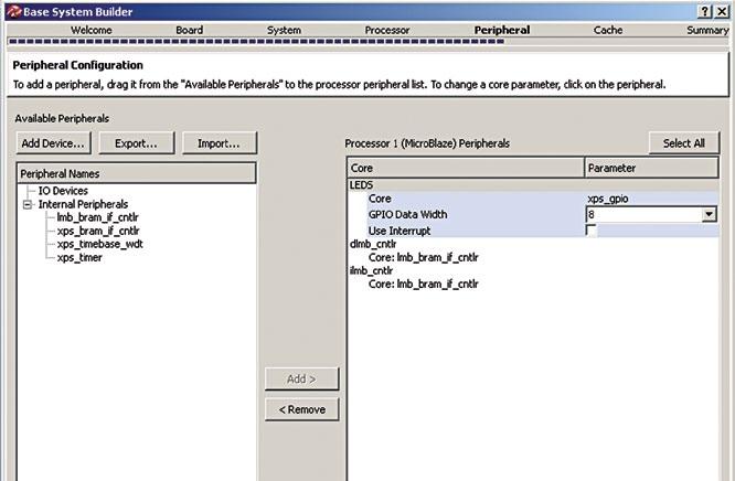
Fig. 8: GPIO data width

Fig. 9: Summary page
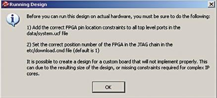
Fig. 10: Custom board configuration generation tool. iMPACT command file is a script file used for downloading bit streams using iMPACT. The IP catalogue contains a list of the peripherals or IP cores that the project has access to. This tab is used when you want to instantiate IP cores into the design. (B) is the Bus-Connectivity area. It shows the interconnections between the different IP cores, memory and the processor. There are two types of buses, namely, the Processor Local Bus (PLB) and the Local Memory Bus (LMB). The vertical line represents a bus and the horizontal line represents a bus interface to an IP core. A hollow connector represents a connection that you can make and a filled connector represents a connection made. To create or disable a connection, click the connector symbol. (C) is the View-Buttons tab. There are two buttons here, using which you can change between Hierarchical view and the Flat view. Hierarchical view is the default view in the System Assembly View panel in which the information about the design is based on the IP core instances in the hardware platform and organised in an expandable or collapsible tree structure. When you click the directory structure icon, the parts are displayed either hierarchically or in a flattened view. (D) is the Console Window area. It displays all the textual information, warnings and errors that occur as the changes are made to the project, netlists and bitstreams, etc. (E) is the System Assembly View in which you can view the project’s IP cores and the properties. It displays all hardware platform IP instances using an expandable tree and table format. The IP elements, their ports, properties and parameters, which are configurable in the System Assembly View, are written directly to the MHS file. There

are three tabs in the System Assembly View, namely, the Bus Interfaces, Ports and the Addresses. The bus interface
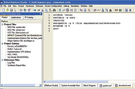
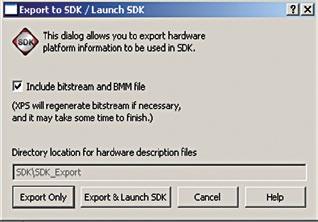
Fig. 13: Download.cmd file
Fig. 14: Export to SDK/Launch SDK
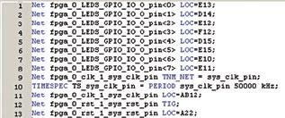
Fig. 15: Workspace Launcher tab shows the following information for each core: (i) Instance name (name of the core used to reference the core in the UCF) (ii) Bus name (the bus to which the core is connected) (iii) IP type (name of the IP core as in the IP catalogue) (iv) IP version (the version of the IP core) The Ports tab shows the user accessible ports of the IP cores and the nets to which they connect. The Addresses tab shows how the IP cores are mapped to the PLBs in the design (F) is the Filters Pane area. It allows you to filter what is shown in the System Assembly View for simplified view of the design or in the case of many IP cores in the design. 16. Since we are using custom board for designing, the UCF file needs to be updated. Allot the FPGA pins to the LEDs, Clock and RST signals. The UCF file created for the ML501 board is shown in Fig. 12. 17. The download. cmd file is changed, as shown in Fig. 13, as the FPGA is the 4th device in the JTAG chain used. (The number assigned depends upon the JTAG being used.) Save the project 18. From the XPS menu, select Project → Export Hardware Design to SDK 19. In the dialogue box that appears (Fig. 14), make sure that Include Bitstream and BMM File are ticked and click Export Only 20. The bitstream will be generated and the project will be exported to SDK subsequently. Once it is done, we can progress to the next step 21. Open SDK by selecting Start → Programs → Xilinx ISE Design Suite 13.4_1 → EDK → Xilinx Software Development Kit 22. The first thing that the designer has to do is to enter the SDK workspace. SDK workspace is a folder wherein the software application(s) for a particular EDK hardware design are managed. The folder specified is shown in Fig. 15. You can choose any folder but it is better if the software folder is created inside the main project folder for ease of use 23. SDK opens with a Welcome screen. Select File → New → Xilinx C Project. Next, you have to specify the hardware platform. Click Specify on the window that appears. In the dialogue box that appears, type the name of the project as edk and use the Browse button under the Target Hardware Specification (refer Fig. 16) heading to navigate to C:\edk\SDK\ SDK_Export\hw\system.xml file.
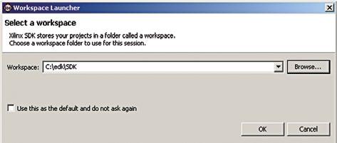

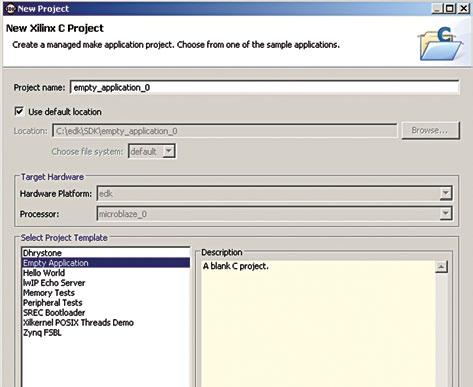
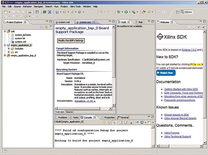
Fig. 18: Xilinx SDK window

Fig. 19: New Source File window Click Finish 24. The wizard that follows allows you to create a template software application for the project. The default is ‘Hello World’ example. We want to create a blank application. Select Empty Application and click Next, as shown in Fig. 17. Click Finish 25. An SDK window appears as shown in Fig. 18 26. In the Project Explorer, open the tree empty_application_0 → src. There is no source file in the folder. We need to add the source file. Select src folder and go to File → New → Source File. In the dialogue box that opens, specify the name of the source file to be created and the folder in which to put it, as shown in Fig. 19. Click Finish. If you now expand the src folder, you will find led.c inside that folder 27. Click on led.c and paste the code given below onto it. Save the file. When you save the file, it is automatically compiled. You should get zero errors, as shown in Fig. 20
The C code first initialises the LEDs port and then sets the port as output port. Then the LEDs are switched on and off using a delay created by the ‘for’ loop

#include “xparameters.h”
#include “xgpio.h”
#include “xutil.h”
//===========Program===========//
int main () {
unsigned long i; //Init LEDS
XGpio LEDS;
XGpio_Initialize(&LEDS, XPAR_LEDS_ DEVICE_ID); XGpio_SetDataDirection(&LEDS, 1, 0x00);
//Out
while (1)
XGpio_DiscreteWrite(&LEDS, 1, 0xFF);
for (i=0; i<0xF0000; i++);
XGpio_DiscreteWrite(&LEDS, 1, 0x00);
for (i=0; i<0xF0000; i++);
return 0;
Select Xilinx Tools → Program FPGA. The bitstream gets loaded to the FPGA. The LEDs start blinking. If they do not blink, press the reset switch used in the design. On pressing the reset switch they will start blinking.
Conclusion
With this part, the series of articles on Designing with FPGAs is concluded. The articles were written with an aim to provide the electronics engineers, professionals and hobbyists an insight into different aspects of system design using FPGAs.
Concluded
Varsha Agrawal is a scientist at Laser Science and Technology Center (LASTEC), a premier DRDO lab working in the field of laser-based defence systems. She has more than 13 years of R&D experience in the design and development of a variety of systems for defence-related applications. She has authored two books and published more than 20 research papers and technical articles

Troubleshooting and Repairing Tips
Do-it-Yourself (DIY) troubleshooting and repairing of electronics gadgets can be fun as it helps you save money and gain useful knowledge. This month we present some websites for the brave hearts who like to troubleshoot and repair electronic devices by themselves
niRaj sahay
fixya.com
FixYa is a community-based troubleshooting resource that provides consumer-generated, practical tips to help consumers solve problems concerning over 12 million products. Fixya is a place where individuals can share real-world experiences and connect to provide each other practical advice. Today, FixYa continues to empower individuals to repair and improve upon their already-purchased possessions. From fixing cars to cameras and iPhones, FixYans are part of a DIY revolution that helps empower techies, tinkerers and hobbyists across the globe.

http://www.fixya.com/

http://www.ifixit.com/
ifixit.com
iFixit is a global community of people helping each other repair things. It was started in 2003 by Luke and Kyle in a dorm room at Cal Poly, San Luis Obispo. It helps thousands of people repair their devices every day. Initially started for Apple products, the website now provides free repair manuals and troubleshooting guides for other products too.
repairfaq.org
Sci.Electronics.Repair frequently asked questions (FAQs) feature Samuel M. Goldwasser’s latest and greatest notes on troubleshooting and repairing. The site is text based and there are no unnecessary, superfluous or useless graphics of any kind. The site covers troubleshooting and repair of consumer electronics equipment.

http://www.repairfaq.org/

http://www.ifitjams.com/
ifitjams.com
When the problem you are trying to fix is not so obvious, it can help to have a flowchart that logically takes you through the process of elimination. The website has details of troubleshooting laptops, PCs and cars based on flowcharts. The site was started by Morris Rosenthal and is a wonderful resource for people who like troubleshooting.
diy-computer-repair.com
The website helps you discover how to troubleshoot, repair, upgrade and maintain your computer. The purpose of this DIY computer-repair website is to assist you with all the information that you may need to troubleshoot and repair your faulty desktop, laptop or server. The site also hosts blogs to share your experiences on fixing problems.

Quality Labs and Certification in Demand
the government of india is pushing the manufacturing industry for a huge surge in exports, and this is leading to the growth of the quality labs and certification industry
SNEHA AMBASTHA
Alab that is completely in line with international requirements and is ISO/IEC 17025 certified is known as a quality lab. Laboratories accredited to this international standard demonstrate their technical competency and ability to produce precise test and/or calibration data.
Testing service labs, such as STQC and TUV SUD, are becoming testing arms for the government of India, where they test and release reports that help the government take the decision on registration of products.
The initiatives taken by the government of India, like the Compulsory Registration Scheme (CRS), would force all the electronics goods of different rating, size and variety to be certified at least once every two years.
“Electronics Test and Development Centre (ETDC), Hyderabad addressed a meet with all manufacturers of electronic goods and promulgated the order ‘Electronics and Information Technology Goods (Requirements of Compulsory Registration) Order, 2012’ which came into effect from April 3, 2013, mandating (testing) compliance of goods to Indian safety standards and compulsory registration with Bureau of Indian Standards (BIS) by the stakeholders, including manufacturers or importers or stockists or distributors,” says P. Chow Reddy, managing director, Interleaved Technologies.
Overall growth factors
The growth of these labs is directly dependent on the requirements of the manufacturing industry.
Export of goods. The government of India is pushing the manufacturing industry for a huge surge in exports,

StrengthS
• The global information • The know-how of the products • The product requirements • The regulatory requirements of various countries
WeakneSSeS OppOrtunitieS
and this is leading to the growth of the quality labs and certification industry. The question is how? All electrical and electronics goods that are to be exported to other countries have to fulfil certain safety norms and certification requirements. The World Trade Organisation (WTO) and Technical Barrier to Trade (TBT) recommend the adoption of these international standards and ensure that they are certified for the same in order to facilitate their trade. Thus the increase in exports is increasing the demand of compliance measures, thereby increasing the demand for quality test labs and certifications. Suresh Kumar, senior vice president, consumer product services, TUV SUD says, “Today, the Indian market is competing with the global expertise on the electronics products where we form a very small part exporting less than one per cent of that of the global exports. Then, there are other factors, like the products manufactured here
meet very little safety criteria as compared to the products from the US or Europe. So the main purpose of labs in India is to assist the manufacturers to meet the safety criteria for their products by transferring the know-how of what they gain globally.” Regional impacts. The productivity of labs in a country is not only dependent on the type of industry, it also has certain regional impact. The policy and regulations for products in any particular region depend on both the consumers and their stakeholders, • High dependence of the labs on such as buyers, induslocal testing and requirements • Less focus on export oriented trial houses, retail martesting and certification kets and other entities Fig. 1: SWOT analysis for quality labs and certification that help maintain the minimum quality level of these products and goods. Each region has its own electrical parameter and environmental conditions which increase the demand for labs with those testing and certification abilities. This helps small regional labs grow, although this growth is not to a large extent. New and upcoming products. Currently, not only in India but all across the world we can see a huge demand for new products with latest technologies. Even the government of India is encouraging new Wi-Fi products along with photovoltaics. Government has also bifurcated the schemes related to electronics into different subsections to encourage the production of new products. Now, as per the schemes, there are new standards that involve new testing tools, testing criteria, new skills and new certification requirements at times. Increased investment by the government in the manufacturing sec-
• Growth of the Indian Electronics Industry • Government subsidiaries and investments • Tax benefits on technology growth • Improvement of India’s share in domestic manufacturing supply
SWOt threatS
• Lot of price erosion in terms of services • Thrilled manpower
Manufacturing testing
•Manufacturing variation •Production defects •QA test tools
Compliance testing apprOVeD
•Lower bar •May not match reality •Static snapshot
electrical stress
•PVT variation •Jitter impact •Electrical Margin
Life testing
•Time variation •MTBF
protocol stress
•Error handling •Random faults •Protocol margin

interop testing
•Define target space •Virtual and real test bed
application stress
•Software interaction •O/S interaction •Cross interfaces
Fig. 2: Different testing approaches by the quality labs (Courtsey: Granite River Labs)
Fig. 3: Expenditures on research and testing (Courtsey: India Brand Equity Foundation (IBEF) manufacture and then get it certified here itself, before taking it back to West or before selling it here in India. This is as opposed to manufacturing it in West and then getting it certified here. So taking the whole South East Asia into consideration, certification enforcement acts as the driving force for
R&D Spending
India’s R&D investment growth is likely to outpace overall GDP growth. During 2010-13, R&D spending (in terms of PPP) was expected to expand at a CAGR of 11.6 per cent to US$ 45.2 billion. 2013E $45 Bn 2012 2011
2010 $40 Bn $38 Bn $33 Bn
tion further adds to production, thus paving a way for the requirement of good, high-end quality labs for testing.
Increasing demand of certification.
If we keep the different aspects aside and look at the certification industry itself, we find that one of the major growth factors for the quality labs is the enforcement of certification. The different schemes by the government, the quality requirements by the consumers and even the industries themselves force manufacturers to get their products certified in order to ensure that they comply with the necessary basic standards. Ankan Mitra, vice-president, SMTA India Chapter explains, “The way this product certification industry works is that, if a company wants to come for manufacturing in India, they would want to this industry.”
Growth of other related industries.
Growth of the electronics industry, IT and software industry, and increasing consumer demands, are all leading to the growth of the quality testing labs and universal certification requirements. If we take the example of mobile phones in India, in 2003 this number was about 18 million, which increased to about 853 million in 2014 and is now expected to grow more than double in the coming years. With this type of growth in the consumer segment, their quality and safety requirements are also increasing.
As per a report by Indian Brand Equity Foundation (IBEF), the labs that have been set up in India and authorised by India’s Standardisation Testing & Quality Certification Directorate (STQC) are supposed to be well equipped to certify the IT systems that are supplied by local and global vendors as safe to connect to the country’s core infrastructure networks. They also reported that the software companies, such as Tech Mahindra and Wipro, have already evinced an interest to set up test labs in India.
Although the growth of the labs in India is slow currently, plenty of factors have come up in the recent years to bring India at par with the other nations
Government policies and their effects
As per a newsletter by the government of India, Department of Electronics
In one of his interviews, Kapil Sibal, Union Minister of Communications and Information Technology said that, with expansion of 3G and 4G/LTE, the requirement of testing labs in India has increased and the ministry would allow self-certification process going forward. He also added that India, with the manufacturing base market of 1.2 billion individuals, needs testing facility within the country and Information Technology (DeitY) and Ministry of Communications and Information Technology, they have come up with a reimbursement scheme for testing and certification required to export electronics goods. The scheme is to support and recognise the micro, small and medium-scale enterprises in the electronic system design and manufacturing (ESDM) sector. Under the scheme, the grant in aid is ` 20 million for 800 models (max) while it is ` 120,000 (max) for one model.
The National Policy on Electronics aims to create an institutional mechanism for developing and mandating standards and certification for electronic products and services to strengthen nation-wide quality assessment infrastructure.
Although these government policies with respect to quality labs do not affect Indian industry, these help the R&D sector grow. As per Reddy, “UL recently started tests in UL 1703 standards, thus facilitating Indian solar PV panels to test and certify.”
IBEF reported that, with respect to the engineering R&D, India is one of the leading offshore destinations in delivering these services with a market share of 22 per cent. The market in India is expected to grow at a compounded annual growth rate of 14 per cent, from $14.7 billion in FY12 to $42 billion by 2020, and is also expected to outpace the information technology growth rate in India.
Challenges in India
To our amazement, while there are plenty of growth factors available, we also see a major threat to this industry, as the labs here are not always well versed with the requirement of test facilities and capabilities.
Lack of test facilities. Considering the manufacturing industry for the domestic, industrial and defence electronics products specially, there are no special test facilities or tools. This leads to the wastage of a large amount of time searching, knowing and getting well equipped with the resources needed. Above all, the labs in India are also short of the latest tools available as
Forecast
Suresh Kumar says, “Most regulations come through governmental organisations globally. However, there are certain segments like automotive, which have a consortium of expertise that bring forth some special standards. For example, Forbes, Clintwear and GM joined together and have come up with some standards for the automotive industry but then restricting myself to the consumer market, the products have to comply with the local government standards or international standards.”
R&D Centres
Bengaluru has 43 per cent of R&D centres
10% 4%
11%
43%
13%
19%
Bengaluru Mumbai/Pune Hyderabad NCR Chennai Others
Fig. 4: Research and development centres in India (Courtsey: India Brand Equity Foundation (IBEF)
compared to the labs abroad.
Lack of skilled manpower. Skilled manpower is somewhat related to the test facilities, as the skills are also required with the usage of the tools and facilities rather than just the implementation of the procedures. Vamshi Kandalla, global GM and VP, Granite River Labs says, “It is but obvious that an individual with strong knowledge in the certifications and test facilities in the country can operate as a consultant to a number of manufacturing industries and development centres.”
No supportive policy for setting
up labs. Although the government has come up with schemes to build a few labs in India, there is no conducive policy for someone setting up a testing lab. Peeyush Gupta, director, sales and marketing, UL says, “In India, setting up a laboratory involves high costs and advanced infrastructure development. In some cases, such as setting up “Overall impact of the government schemes and policies is not affecting the Indian industry but the R&D section of the industry” —P. Chow Reddy
Challenges to the industry are not few, but a better understanding between the government of India and the private testing labs can help eliminate the major challenges
“UL is committed to working with manufacturers, industry associations and government bodies to accelerate adoption of safety standards and certification procedures. Our aim is to ensure that the consumer has access to high-quality products as a result of regulatory testing and standardisation of products and services.” —Peeyush Gupta
a top-quality mobile testing laboratory or a wireless testing laboratory, the cost varies between 200 million and a billion rupees. Unfortunately, there are no existing regulatory policies or government schemes that support infrastructure development or incentivise quality facilities to address specific market regulations.” Sometimes, it is difficult to set up a lab as the kind of infrastructure required for this is so immense.
From tens of millions of rupees, some can require ` 500 million investment. One is required to spend anywhere from ` 2000 million to ` 5000 million to set up a good-quality mobile testing lab or a wireless testing lab.
Lack of public private relationship.
There are some private labs in India that are working in the field of testing since over 100 years in a global environment. They have a lot of knowledge and expertise for not only testing but also for standard-to-standard citing. Generally, the Indian government looks at these private labs only for innovation testing or infrastructure.
The government should open up in terms of policies and standards for private players. There is a need of firm commitment in terms of regulations,

Labs to come up
Government of India has planned to set up some labs in India to support the growth of the electronic system design and manufacturing (ESDM) industry at a CAGR of 9.9 per cent. In view of this, the Department of Electronics and Information Technology (DeitY) has been proposed to invest ` 650,000 million in the area of manufacturing of electronics and semiconductors. Thus the first lab on semiconductor characterisation in India is expected to be set up in Bengaluru in the next six months, the success of which would lead to the set up of another lab in Bhubaneswar that is expected to be launched in next one year.
A report on Karnataka ESDM policy suggests that the government has decided to set up three ESDM innovation centres within Karnataka. The main idea behind these centres is to provide facilities for testing and development, to have characterisation labs, and compliance and certifications labs. The first amongst these would be housed at IIIT Bengaluru.
Another report by India Electronics and Semiconductor Association (IESA) suggests that BIS is to set up a test lab in Khurda cluster to help the preferential access to the products that are manufactured in India.
Major Contributors to this report
Ankan Mitra,
vice-president, SMTA India Chapter
C.S. Bisht,
scientist ‘G’ and senior director, IT Centre, STQC Delhi
P. Chow Reddy,
managing director, Interleaved Technologies
Peeyush Gupta,
director, sales and marketing, UL
Suresh Kumar,
senior vice president, consumer product services, TUV SUD
Vamshi Kandalla, global GM and VP, Granite River Labs
2595 2898 3151 3099 2964
2008-09 2009-10 2010-112011-122012-13 BIS Product Certification Licences granted
Fig. 5: Product certificate licences (Courtsey: BIS)
policies and incentives from the government. Otherwise, it becomes very difficult for the industry to come forward and take the initiative or to make the first move.
Consider a situation where there is a small change in standards by BIS and the private test labs have not been informed about it in time. They may have tested 500 products by the time the new standard is announced. Now what should the test labs do with the 500 test reports? There would be extra time and manpower required to test according to the new standards for the correct certification.
Gupta explains, “Over the last few months there have been several requests pertaining to certified components, power supply and power cords. These requirements have not been restricted to just UL but were also applicable to other private, ERTL or government labs, with instances where reports have had to be withdrawn and revised accordingly.”
Solutions implemented
The manufacturing sector is taking steps to see that they adopt sustainable practices. The labs now ensure that their services are not limited to testing but they also support the manufacturers for proper systems implemention. The labs are also ensuring that the manufacturers follow proper social compliance standards and maintain certain occupational safety in their work premises.
As per a report by BIS, they are taking certain basic measures to ensure the growth of the labs and the certification industry, which includes training and the labs’ recognition schemes. There are regular trainings for the manpower working in the labs to ensure their awareness of latest developments on international platforms. BIS is training officers from its own labs on international standards like IS/ ISO/IEC 17025 and is also providing summer training to the students from different universities and colleges on the laboratory-related works.
BIS has also come up with the Laboratory Recognition Scheme (LRS) that helps the outside laboratories (OSLs) to get recognition. These OSLs are the ones that help labs like BIS with testing facilities during situations such as a large number of samples for testing, or BIS testing equipment being out of order. In order to support this scheme, about seven OSLs have been recognised in the year 2012-13 to test products covered under electronics and information technology goods, such as IT (IS 13252), AV (IS 616) and microwave ovens (IS 302-2-25).
C.S. Bisht, scientist ‘G’ and senior director, IT Centre, STQC Delhi says, “STQC has come up with the scheme for approval of IT test laboratories (ITTLs) for software solutions. STQC will be the nodal agency managing this approval scheme. The scheme requires ITTLs to implement a domain-specific laboratory ‘Quality Management System’ based on ISO/IEC 17025 standard. The IT test laboratory will be assessed as per ISO/IEC 17025 general requirements for the competence of testing and calibration laboratories. ITTLs will also be assessed as per ISO/IEC 25051 (ISO/ IEC 29119 under development) for test management activities. STQC approval body (ITTL) will operate as per ISO/ IEC 17011: 2004 standard ‘Conformity Assessment-General requirement for accreditation bodies accrediting conformity assessment bodies’.”
Vamshi adds, “There are a number of OSLs in India presently that cannot be compared to the giant service and solution providers, though they have their own value and their existence here is important as per the requirements.”


