3 minute read
Exploring Millimeter-Wave Interconnect for Chip-to-Chip Communication


By M. Meraj Ahmed
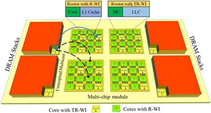
With aggressive scaling of device geometries, yield of complex Multi-Processor Systems-on-Chips (MP-SoCs) will decrease due to higher probability of manufacturing defects. Disintegration of large SoCs into smaller chips called chiplets will improve yield and cost of complex platform-based systems. AMD’s EPYC which was released in 2017, is an example of such multichip system having 4 chiplets. However, performance of multichip systems is limited by the off-chip I/Os as they provide high power and latency overheads. On the other hand, millimeter-wave (mm-wave) wireless interconnects can establish single hop communication between multiple chips to provide high speed and energy-efficient communication. Fig. 1 conceptualize such multichip communication. Here, we briefly discuss the architecture and how to leverage mm-wave interconnect for multichip communication.
Fig. 1. Multichip communication using mm-wave interconnect.
(a)
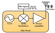
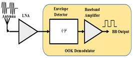
Fig. 2. Block diagram of the OOK (a) Transmitter, (b) Receiver. (b)
System and Wireless Interface (WI) Architecture: We consider a tile-based multicore-multichip (MCMC) architecture typically used in high performance computing nodes such as server blades. Each tile in the MCMC system is composed of a processing core, a switch, L1 private cache and a distributed shared last level cache (LLC). Tiles in each chip are connected with each other through a regular wired mesh-based Network-on Chip (NoC). For inter-chip communication, in each chip, we equip some or all the NoC switches with WIs as shown in Fig. 1. A WI can have both Transmitter (Tx) and Receiver (Rx) circuitry or can have only Rx circuitry. We call such WI as TR-WI and R-WI respectively and shown in Fig. 1. The Tx used in a WI typically consists of Voltage Controlled Oscillator (VCO), modulator, Drive Amplifier (DA) while the Rx circuitry includes Low Noise Amplifier (LNA), Envelop Detector (ED) and Baseband Amplifier as shown in Fig. 2. As modulation technique On-Off Keying (OOK) along with a zig-zag antenna have been chosen due to their low implementation overhead.
18
| The ROCHESTER ENGINEER OCTOBER 2020 feature student article
Enhancing Multicast-Broadcast Performance for on and off-chip Communication:
In MCMC system with an in-package memory module as shown in Fig. 1, traffic pattern not only consists of core to core unicast (one-to-one) messages but also significant memory to core multicast/broadcast (one-to-many) messages. Directory or snooping based cache coherency protocols in a shared memory MCMC system use multicast to invalidate a shared cache block or broadcast the updated block for the requesting cores. Moreover, many control signals such as passing global states, power gating, and barrier synchronization, novel computing paradigms such as spiking neural network and genetic algorithms could be also multicast driven. Traditional wired based MCMC architectures are multi-hop in nature and provide very limited support for multicast/broadcast traffic whereas mm-wave interconnects provide inherent multicast/broadcast support to provide low latency and energy for such messages. Simulation results in Fig. 3 show that the mm-wave interconnect outperforms wired interconnect in terms of average latency and energy consumption for various application specific traffic patterns.
Fig. 3. (a) Latency (b) Energy comparison between mm-Wave and Wired interconnect.
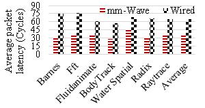
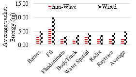
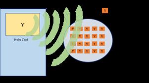
Fig. 4. A conceptual view of wireless wafer testing.
Reducing Test Time for Complex SoCs:
Wafer-level testing presents huge challenges to high fault-coverage due to severely restricted controllability and observability, especially for complex SoCs or multicore processors. Traditionally wafer-level testing is restricted to basic tests using probes. The probe needles come in physical contact with the wafer and can cause damage to the wafer due to the stress applied by the probes. On-chip mm-wave transceivers can receive test data from an external equipment such as an Automatic Test Equipment (ATE) which will also be equipped with a wireless transceiver to send and receive test data and response respectively. This wireless test mechanism is shown in Fig. 4. Depending on the speed of the chosen physical and control layer efficiency, test data can be delivered at high rates to uncut dies in the wafer without requiring physical contact.
M Meraj Ahmed is currently pursuing his Ph.D. at Rochester Institute of Technology, USA.
His research interest includes designing energy-efficient and low latency broadcast-oriented
interconnection architecture for multicore, multichip communication. He is also interested about
designing a secure and reliable mm-Wave multichip wireless communication.
feature student article OCTOBER 2020 The ROCHESTER ENGINEER |


