4 minute read
Droplet based metal additive manufacturing process as a cost-effective technique for fabrication of high-performance flexible electronics


By Manoj Meda
The world has witnessed three industrial revolutions in the last 300 years resulting in a tectonic shift in the way in which we live. Among them the third and most recent is the digital revolution, that began in the 1950’s, which brought electronic devices, semiconductors, mainframe/personal computing, and the internet. The advent of electronic devices led to disruption of all the vital avenues of the global economy such as healthcare, energy, transportation, communication etc. The key driver for ubiquity of electronic devices around us, can be attributed to the advancements in manufacturing processes such as photolithography, which enabled manufacturing of more powerful, smaller, and affordable integrated circuits in every iteration. We are currently at the dawn of the 4th industrial revolution, which is poised to disrupt and profoundly transform the electronics landscape with the Internet of Things (IoT). IoT can be described as a network of diverse physical devices embedded with electronics, that can connect, collect, and exchange data in real time. This would integrate the physical world into the digital world and result in significant increase in productivity, incremental economic benefits, and reduced human efforts. One of the key drivers for IoT would be the light weight and extremely cost-effective flexible electronic devices. The flexible nature of these devices will make them very well suited to be used in numerous areas where the current rigid electronics cannot be employed. Flexible electronics, with intriguing properties such as softness and ductility have broad application prospects such as intelligent packaging, low cost RFID (radio-frequency identification) transponders, flexible displays, flexible solar cells, flexible batteries, disposable diagnostic/monitoring devices etc. In addition to that the substrates used for flexible electronics - such as polymers or paper - tend to be significantly cheaper than the widely used rigid substrates such as silicon wafers or glass. This makes these devices considerably cheaper.
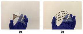
Additive manufacturing processes such as materialsbased inkjet printing techniques are currently being employed for fabricating flexible electronic circuitry. These techniques are typically employed to deposit metal nanoparticles suspended in suitable solvents –referred to as metal-based inks - onto flexible polymer substrates, in a precise manor to form the electrical circuits. Figure 1 shows an RFID tag and some electrodes printed using a copper nano particle ink
onto polyethylene terephthalate (PET) substrate.
16
| The ROCHESTER ENGINEER OCTOBER 2020
Figure 1: (a) RFID tag and (b) Electrodes printed using copper nano particle ink.
However, this approach poses three major limitations. First, the printed features typically require post processing techniques - such as thermal sintering - wherein they are subjected to elevated temperature to render them electrically conductive. Second, the cost of the raw materials i.e. the nanoparticles tend to be about 2 orders of magnitude higher than the cost of the actual metal - thereby driving the final product cost upwards. Third, the printed features generally tend to have lower electrical conductivity than the metals that are used as the raw material.
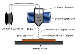
We studied the direct deposition of molten metal droplets onto high performance polymer substrates, as a way of addressing the major limitations with the current approaches. As illustrated in Figure 2, droplets of molten aluminum alloy 4043 were deposited through a magneto hydrodynamic metal jetting process - manufactured by Xerox Corporation, Rochester, NY, USA - onto a flexible polyimide substrate for the purpose of fabricating electronic
feature student article
circuits. By optimizing the process conditions –
such as overlap percentage between adjacent
droplets, deposition frequency, temperature of the droplet, temperature of the substrate etc. – through experimental studies and numerical modelling, we
metal droplets can be successfully deposited onto polymer substrates for the purpose of fabricating flexible electronics.
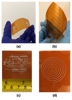
Figure 2: Cross sectional view of printhead in the magneto hydrodynamic metal jetting process and process overview.
As metal droplets solidify on the polymer substrate, they inherently become highly electrically conductive without the need for any post processing. The raw material used in this process is in the form of wire. The aluminum wire is about 2 orders of magnitude cheaper by weight than aluminum nanoparticles. This makes the process significantly cheaper than the conventional approach for printing electronic circuits through solvent based metal nanoparticle inks. Most importantly this approach enables achieving bulk metal electrical conductivity which is extremely difficult to achieve through metal-based inks.
Figure 3 shows circuits printed onto polyimide substrate through the magneto hydrodynamic metal jetting process using aluminum 4043 alloy. The printed features demonstrate excellent adhesion and surface roughness comparable to printed circuit boards currently being used in the industry.
Figure 3: (a) RFID tag (b) serpentine circuit (c) microcontroller circuit and (d) induction coil printed using the magneto hydrodynamic metal jetting process.
Through our research we have demonstrated that molten metal jetting process is a viable technique for fabricating highly electrically conductive circuits onto flexible polymer substrates. Further research is needed in terms of improving the feature resolution of printed features – which currently stands at ~200μm. Extending the research to studying the deposition of widely used metals such as copper onto cheaper substrates such as PET could enable low cost manufacturing of flexible electronic circuits for numerous applications in the IoT.
Manoj Meda is a PhD candidate in the Industrial and systems Engineering Department at Rochester Institute of Technology.
feature student article OCTOBER 2020 The ROCHESTER ENGINEER |


