THE TOPOLOGICAL QUBIT
In his extensive UCSB lab, Professor Chris Palmstrøm (electrical and computer engineering, and materials) uses molecular beam epitaxy to combine elements to grow single-crystal compounds on singlecrystal wafers, what he describes as “making designer materials with novel properties.” He also makes thin films of materials that have been found, in bulk form, to have interesting and potentially useful characteristics. “We’re interested in what happens at the interface when different materials are put together,” he says. “It may be that electrons behave in some novel way at the surface of a new bulk material, so, if we interface that with something else, maybe we can use the combined states to do novel things. Or, we can combine two more-normal materials to produce an interesting effect.” Currently, his lab team is attempting to put a superconducting material — one that conducts with 100-percent efficiency because it has no electrical resistance and no electronic field — onto a semiconductor material to see if the semiconductor can be made into a superconductor and create a novel electronic state called a Majorana fermion. It’s related to Microsoft’s approach for creating a topological quantum computer, but, says Palmstrøm, as is always the case at the leading edge of material science, “There are always plenty of challenges.”
THE CHEMISTRY OF MATERIALS FOR QUANTUM INFORMATION In working with materials for quantum information systems, professor of materials and chemistry Ram Seshadri focuses on topological quantum materials, that is, materials whose electronic structure can protect a coherent state essential to quantum operations. “The starting point for everyone in this area is, typically, to perform an electronic structure calculation using the formalism developed by the late UCSB professor Walter Kohn.” (Kohn shared the Nobel Prize for this work.) From there, he says, “When we find some interesting new-material candidates, and we try to make them in the lab and measure some of their properties. Then, ideally, we hand the material off to someone like [materials associate professor] Stephen Wilson, who can develop it further.” For some quantum materials, he adds, “We ask, what are the chemical origins of their particular properties, because we think that by learning the chemistry, we can develop some predictive control. The physics is the useful outcome; the chemistry is how you get there.” Seshadri also believes that, by understanding materials for quantum information systems, it is possible to gain insights into materials for energy conversion and storage systems, such as photovoltaics, magnets, and thermoelectrics. There have already been some suggestions that a certain class of materials for quantum information systems could also perform well as thermoelectric materials, and vice versa.”
ON THE THIN-FILM FRONT
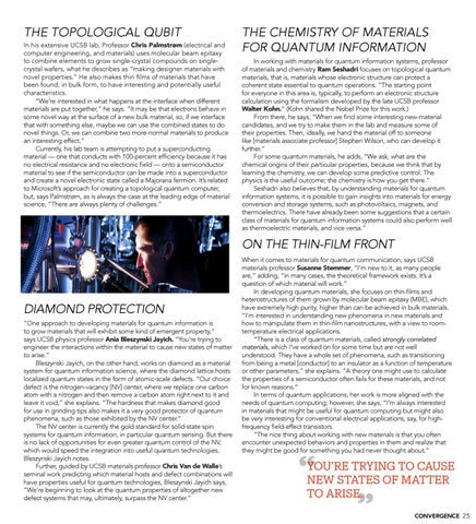
DIAMOND PROTECTION “One approach to developing materials for quantum information is to grow materials that will exhibit some kind of emergent property,” says UCSB physics professor Ania Bleszynski Jayich. “You’re trying to engineer the interactions within the material to cause new states of matter to arise.” Bleszynski Jayich, on the other hand, works on diamond as a material system for quantum information science, where the diamond lattice hosts localized quantum states in the form of atomic-scale defects. “Our choice defect is the nitrogen-vacancy [NV] center, where we replace one carbon atom with a nitrogen and then remove a carbon atom right next to it and leave it void,” she explains. “The hardness that makes diamond good for use in grinding tips also makes it a very good protector of quantum phenomena, such as those exhibited by the NV center.” The NV center is currently the gold standard for solid-state spin systems for quantum information, in particular quantum sensing. But there is no lack of opportunities for even greater quantum control of the NV, which would speed the integration into useful quantum technologies, Bleszynski Jayich notes. Further, guided by UCSB materials professor Chris Van de Walle’s seminal work predicting which material hosts and defect combinations will have properties useful for quantum technologies, Bleszynski Jayich says, “We’re beginning to look at the quantum properties of altogether new defect systems that may, ultimately, surpass the NV center.”
When it comes to materials for quantum communication, says UCSB materials professor Susanne Stemmer, “I’m new to it, as many people are,” adding, “in many cases, the theoretical framework exists. It’s a question of which material will work.” In developing quantum materials, she focuses on thin-films and heterostructures of them grown by molecular beam epitaxy (MBE), which have extremely high purity, higher than can be achieved in bulk materials. “I’m interested in understanding new phenomena in new materials and how to manipulate them in thin-film nanostructures, with a view to roomtemperature electrical applications. “There is a class of quantum materials, called strongly correlated materials, which I’ve worked on for some time but are not well understood. They have a whole set of phenomena, such as transitioning from being a metal [conductor] to an insulator as a function of temperature or other parameters,” she explains. “A theory one might use to calculate the properties of a semiconductor often fails for these materials, and not for known reasons.“ In terms of quantum applications, her work is more aligned with the needs of quantum computing; however, she says, “I’m always interested in materials that might be useful for quantum computing but might also be very interesting for conventional electrical applications, say, for highfrequency field-effect transistors. “The nice thing about working with new materials is that you often encounter unexpected behaviors and properties in them and realize that they might be good for something you had never thought about.”
“
YOU’RE TRYING TO CAUSE NEW STATES OF MATTER TO ARISE.
”
25