Introduction to Digital Logic and Components
MISSOURI UNIVERSITY OF SCIENCE AND TECHNOLOGY
R. JOE STANLEY & ROBERT S. WOODLEY
2023
Table of Contents Chapter 1: Binary Codes and Number Systems 6 Chapter 1 Learning Goals .......................................................................................................................... 6 Chapter 1 Learning Objectives .................................................................................................................. 6 1.1 Overview of digital systems and design 7 1.2 Number Systems ............................................................................................................................... .. 8 1.2.1 Binary 9 1.2.2 Octal and Hexadecimal .............................................................................................................. 10 1.3 Number Representations in Digital Systems .................................................................................... 10 1.3.1 Successive Divisions 11 1.3.2 Successive Multiplications ......................................................................................................... 12 1.3.3 Binary, Octal, and Hexadecimal Conversions 15 1.4 Signed Numbers – r’s Complement Approach 16 1.4.1 2’s Complement Integer Representation ................................................................................... 17 1.4.2 2’s Complement for Fractional Values 19 1.4.3 2’s Complement Addition and Subtraction ................................................................................ 20 1.4.4 2’s Complement Value Ranges and Arithmetic Overflow 21 1.5 Binary Encoding Schemes 22 Chapter 2: Boolean Algebra ....................................................................................................................... 24 Chapter 2 Learning Goals 24 Chapter 2 Learning Objectives ................................................................................................................ 24 2.1 Overview of Digital Circuits 25 2.2 Logic Operators 26 2.2.1 NOT Operator ............................................................................................................................. 26 2.2.2 OR Operator 27 2.2.3 AND Operator ............................................................................................................................ 27 2.2.4 NAND Operator .......................................................................................................................... 28 2.2.5 NOR Operator 28 2.2.6 Exclusive‐OR (XOR) ..................................................................................................................... 28 2.2.7 Exclusive‐NOR (XNOR) Operator 29 2.3 Logic Identities and Algebraic Laws .................................................................................................. 30 2.4 DeMorgan’s Theorems ...................................................................................................................... 32 2.5 Logic Functions and Networks 33
2.6 Digital Circuit Implementation .......................................................................................................... 33 2.7 Design Problem Word Problems 36 2.8 Logic Function Simplification Using Boolean Algebra ....................................................................... 39 2.9 Complete Logic Sets .......................................................................................................................... 45 2.9.1 NAND‐BASED Logic..................................................................................................................... 46 2.9.2 NOR‐BASED LOGIC ..................................................................................................................... 48 Chapter 3: Structured Forms and Karnaugh Maps 51 Chapter 3 Learning Goals ........................................................................................................................ 51 Chapter 3 Learning Objectives ................................................................................................................ 51 3.1 Structured Logic 52 3.1.1 Sum of Products ......................................................................................................................... 52 3.1.2 Product of sums (POS) 53 3.1.3 Minterms ............................................................................................................................... ..... 55 3.1.4 Maxterms ............................................................................................................................... .... 56 3.2 Karnaugh Maps 58 3.2.1 2 Variable K‐Maps ..................................................................................................................... 58 3.2.2 3 Variable K‐Maps 61 3.2.3 Don’t Care Conditions ................................................................................................................ 64 3.2.4 4 Variable Karnaugh Maps ........................................................................................................ 65 3.3 Seven‐Segment Display and Example Design Problem 70 Chapter 4: CMOS Logic Circuits .................................................................................................................. 73 Chapter 4 Learning Goals ........................................................................................................................ 73 Chapter 4 Learning Objectives 73 4.1 Overview of Logic Families ................................................................................................................ 74 4.2 Overview of CMOS 74 4.2.1 MOSFETs ............................................................................................................................... ..... 74 4.3 CMOS inverter ............................................................................................................................... .... 77 4.4 Transistor Connections 78 Chapter 5: Digital Components .................................................................................................................. 87 Chapter 5 Learning Goals 87 Chapter 5 Learning Objectives ................................................................................................................ 87 5.1 Comparison of binary numbers ........................................................................................................ 88 5.1.1 Equality Comparator 88
5.1.2 Magnitude Comparator ............................................................................................................. 91 5.2 Decoders 93 5.2.1 Active‐High Decoder .................................................................................................................. 93 4.2.2 Active‐Low Decoder ................................................................................................................... 95 5.2.3 Combinatorial Functions Using Decoders 96 5.2.4 Expanding Decoder Capability ................................................................................................... 99 5.2.5 Multiple Functions Using One Decoder 102 5.3 Multiplexor Devices ........................................................................................................................ 103 5.4 Complex Functions Using Digital Components ............................................................................... 105 5.5 Combinatorial Functions with Multiplexors 107 5.6 De‐multiplexors and Encoders ........................................................................................................ 112 5.6.1 Encoder 112 5.6.2 De‐multiplexor ......................................................................................................................... 113 5.7 Adders ............................................................................................................................... .............. 114 5.7.1 Adder operation 114 5.7.2 Subtraction with Adders .......................................................................................................... 118 5.7.3 More Fun with Adders ............................................................................................................. 119 5.8 Programmable Logic Arrays ............................................................................................................ 122 5.8.1 Programmable Types and Conventional Symbols ................................................................... 122 5.8.2 OR/AND PLA 123 5.8.3 AND/OR PLA ............................................................................................................................. 124 5.8.4 PLA’s with minterm and maxterm functions ........................................................................... 125 5.8.5 Implementing simplified functions in a PLA 126 Chapter 6: Memory Elements .................................................................................................................. 129 Chapter 6 Learning Goals 129 Chapter 6 Learning Objectives .............................................................................................................. 129 6.1 Latch ............................................................................................................................... ................. 130 6.2 Set (S) Reset(R) Latch 130 6.2.1 NOR SR Latch ............................................................................................................................ 131 6.2.2 NAND SR Latch 132 6.2.3 D Latch ............................................................................................................................... ...... 133 6.3 Clocked Latches as Memory Elements ............................................................................................ 133 6.3.1 Clocked SR Latch 133
6.3.2 Clocked D Latch ........................................................................................................................ 135 6.4 Flip Flop 137 6.4.1 Rising and Falling Edge Enable/Clock Transitions .................................................................... 139 6.5 Flip Flop Definitions ........................................................................................................................ 140 6.5.1 D Flip Flop 140 6.5.2 SR Flip Flop ............................................................................................................................... 141 6.5.3 JK Flip Flop 142 6.5.4 T Flip Flop ............................................................................................................................... .. 142 6.5.5 Example Timing Diagrams ........................................................................................................ 143 6.6 Flip Flop Applications 145 6.7 Random Access Memory ................................................................................................................ 148 6.8 Arithmetic and Logic Operation Temporary Storage 153 Chapter 7: State Machines ....................................................................................................................... 158 Chapter 7 Learning Goals ...................................................................................................................... 158 Chapter 7 Learning Objectives 158 7.1 Overview of Finite State Machines ................................................................................................. 159 7.2 Sequential Circuits with 1 or 2 State Variables 161 7.3 Mealy and Moore Machines ........................................................................................................... 167 7.4 Sequential Circuit Design ................................................................................................................ 168 7.4.1 Sequential Circuit Design Process 169 7.5 State Machine Examples ................................................................................................................. 172
Chapter 1: Binary Codes and Number Systems
Chapter 1 Learning Goals
Identify what is a digital system.
Identify, represent, and convert numbers using different number systems that are related to digital systems.
Perform arithmetic operations using different number systems that are related to digital systems.
Chapter 1 Learning Objectives
Define digital systems
Define digital system design
Define and represent numbers using different number bases
Add, subtract, divide, and multiply numbers using different bases
Convert numbers between bases
Define and represent signed binary numbers using 2’s complement
Add, subtract, and multiply binary numbers using 2’s complement
Represent and use binary fractions
Define binary encoding schemes
1.1 Overview of digital systems and design
Digital circuit design integrates user identifiable inputs with digital components to process the inputs for generating user identifiable outputs. User identifiable inputs may be keys on a keyboard, on/off switches, buttons on a remote control, temperature sensors, joysticks to perform movement, tire pressure sensors, door and window sensors for a security system, light or motion sensors, among many others. User identifiable outputs may be turning on/off light emitting diodes (LEDs), audible speaker sounds, turning on/off electric motors, turning on/off household appliances such as microwave ovens or washing machines, among many others. Note that the inputs use electrical components, analog and/or digital, that must be converted to a form that can be used in a digital system to generate the outputs. The outputs may require electrical components to represent the operation using the digital circuit.
Digital circuit design requires exposure to electronic circuits and devices used as inputs and outputs, as well as the digital components, which are much of the focus of this book! If you have ever taken off the cover of a remote control, cell phone, computer, furnace, electronic toys, etc., you were likely to see a green printed circuit board (PCB). An example of a PCB is shown in Fig. 1-1 below. The PCB has a number of components including the power supply, integrated circuits (digital components), connectors or user input/output peripherals. Some of these items are highlighted.
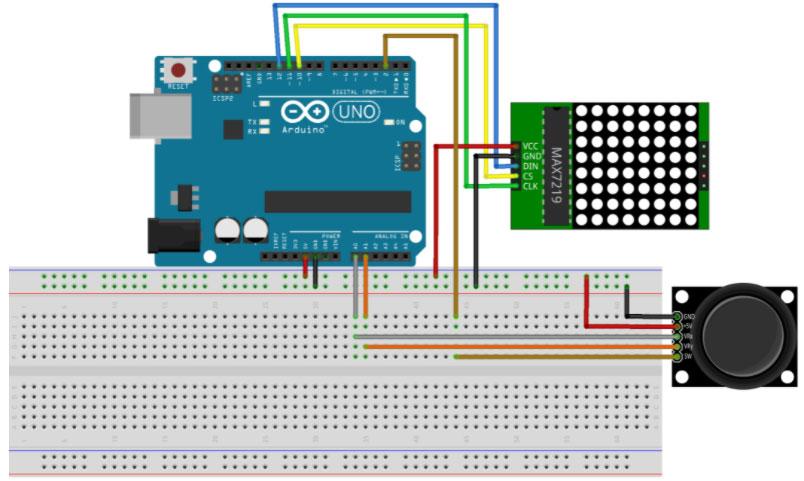
A circuit example with a joystick and 8x8 matrix display connected to an Arduino Uno computer board is shown in Fig. 1-2 below. The joystick and matrix display are connected to the Arduino Uno computer board using a prototyping device called a breadboard. A breadboard provides a row and column structured layout for wire connections between the different components in the circuit. Joysticks are analog input devices that have electrical components called potentiometers provide x and y axis position changes. These x and y potentiometers are connected to analog to digital converter (ADC) circuits to provide values that can be used in a digital circuit. The 8x8
 Fig. 1‐1. Printed circuit board example with components1
matrix display is an output peripheral device that is used in this example circuit to display the joystick movements.
Extending the above illustrations, digital logic design involves the use and integration of electrical and physical components with electrical and computer properties such as power, current, voltage, logical operation, protocol or convention, and user interface.
This textbook will explore different facets of digital circuit design. We will begin in this chapter examining different data encoding schemes that can be used as inputs or outputs of digital circuits. The data encoding schemes also provide the basis for performing and interpreting data values in digital circuits.
1.2 Number Systems
Decimal: 0-9 (base 10)
Binary: 0, 1 (base 2)
Hexadecimal (hex): 0-9, A, B, C, D, E, F (base 16)
Octal: 0-7 (base 8)
In this section, commonly used number systems in digital systems are examined, including binary (base 2), decimal (base 10), hexadecimal (base 16), and octal (base 8) number systems and how to convert numbers from one base to another. The counting digits for these number systems, bases, for number representation are shown (right). Note that since hexadecimal is base 16, we represent the numbers 10 through 15 with the symbols A, B, C, D, E, F so that each position is only occupied by a single character.
Fig. 1‐2. Digital system input examples2
With decimal as the base for number representation, the number can be expressed as a power of 10 sum as illustrated:
210 power of 10 positions
943(10) = 3x100 + 4x101 + 9x10²
Each base 10 number digit corresponds to a power of 10 position, starting with the rightmost digit (to the left of the decimal point which is implied in this case since this number is an integer) as 100, the next digit to the left is the next power of base 10 as 101 increasing the power of the base going from right to left), and so on. The value 943 decimal is the weighted sum of base 10 raised to the power position times the corresponding digit in base 10 over all of the digit positions in the number. The conversion of 943 decimal (base 10 given in ()) is shown above with the powers of 10 given above each decimal digit.
Below is an example for representing a binary (base 2) number and its conversion to decimal (base 10).
3210 power of 2 positions
1011(2) = 1x20 + 1x21 + 1x22 + 1x23 = 1+2+8 = 11(10)
The binary number 1011 is shown with powers of 2 above each digit and the associated weighted sum translating each binary digit and power of 2 value into decimal to obtain the decimal representation.
We now look at fundamental arithmetic operations, addition and subtraction, for number representation in different bases. Consider the following decimal addition example, 254 + 697. Starting with the rightmost digit position, add the decimal digits. Adding 4 and 7 to get 11, since 11 is greater than the base 10, the base 10 is subtracted from the digit sum. So, 11 (digit sum) – 10 (base) = 1, which is a base 10 digit that is given as the sum digit with a carry of 1 to the next digit position to the right. Adding 5 and 9 and the carry of 1 from the previous digit addition gives a sum of 15. Since this sum is greater than or equal to the base 10, the base 10 is subtracted from the sum of 15 to get 5. The digit 5 is put in this sum position with a 1 carry out to the next digit position. Finally, 2 and 6 and the carry out 1 are added for a sum of 9. Since 9 is less than the base 10, i.e. a valid digit for base 10, the base 10 does not need to be subtracted from 9, and there is no carry (or carry out of 0) for the next digit position. The value 9 is for the digit in the sum.
1.2.1 Binary
Consider applying the same approach to adding binary numbers. In the example below, 0111 (7 decimal) is added to 0011 (3 decimal). Adding the rightmost digits 1 and 1 to get 2. Two is greater than or equal to the base 2, so the base 2 is subtracted from the sum of 2 to give 0, which is put in this sum digit position and 1 is carried to the next digit position to the right. For the next binary digit position (bit position), the digits 1 and 1 and the carry out 1 are added to give 3, which is
1 1 254 11 +697 ‐10 951 1
subtracted from the base 2 to get a value of 1 put in this digit position for the sum. A 1 is carried out to the next bit position. The process is repeated to generate the base 2 sum of 1010 (base 10 value of 10).
Accordingly, this approach is applied to adding numbers for different bases. Below are addition examples for octal and hexadecimal numbers, respectively.
1.2.2 Octal and Hexadecimal
Starting with the least significant (rightmost) position, 6+4 in octal equals 10 in decimal. Since 10 is above the highest counting digit (7) in octal, subtract the base 8 from the decimal sum value (10-8) to get the octal sum digit 2 with a carry of 1 to the next digit position. Adding the carry and octal digits in the next position (1+5+2) gives 8 in decimal. Since the sum is above 7, subtract the base 8 from the decimal sum value (8-8) to find the octal sum digit 0 with a carry of 1 to the next digit position. Adding the octal values 1 (carry)+7+0 yields 8, which is adjusted (8-8) to 0 with a carry out of the most significant digit of 1. The final sum is 1002 (octal).
For hexadecimal addition, consider A5F+2CB. Again, start with the sum for the least significant digit, F+B, which is a decimal sum of 15+11=26. Since 26 is greater than the highest hex digit (F) decimal value (15), Using the process to perform decimal number addition can be applied to other number bases. In a similar fashion, use the process to perform decimal number subtraction for other bases.
Examples of subtraction for decimal, binary, octal and hexadecimal bases are shown below with borrowing to determine digit values.
1.3 Number Representations in Digital Systems
Most digital systems use binary as the basis for operations performed. The following is terminology commonly used with binary values. Each individual binary digit is referred to as a bit. The number of bits, n, is denoted as an n-bit binary word. An 8-bit word is referred to as a byte. In an 8-bit word (as illustrated below), the upper 4 bits and lower 4 bits are designated as the upper (blue) and lower (yellow) nibbles, respectively.
1 1 1 0111 2 3 2 +0011 ‐2 ‐2 ‐2 1010 0 1 0 1 1 1 756 10 8 8 + 024 ‐8 ‐8 ‐8 1 002 2 0 0 1 1 A5F 15 18 + 2CB +11 ‐16 D2A 26 2 ‐16 10 (A) Decimal Binary Octal Hex 1 10 5 11 0 2 0 2 5 2 8 11 24 861 1010 630 C8F ‐ 447 ‐ 0111 ‐ 177 ‐1AB 414 0011 431 AE4
1110 1010 (8-bit word)
Given the 8-bit word, 1110 1010. This value by default is an unsigned, so the decimal equivalent is given as: 0x20 + 1x21 + 0x22 + 1x23 + 0x24 + 1x25 + 1x26 + 1x27 = 234 decimal.
In the example above, the 8-bit binary word is converted to its decimal equivalent. In the context of working with other number systems, particularly those associated with digital systems, converting the values from other number systems to decimal is of interest for user (human) interpretation of values. In the encoding of numbers from other bases, the numbers may contain integer and/or fractional values. In converting decimal values to other bases, two iterative methods are presented:
1) Successive divisions to convert the integer portion of a decimal number.
2) Successive multiplications to convert the fractional portion of a decimal number.
1.3.1 Successive Divisions
The method of successive divisions is used to convert integer portions of numbers to their decimal representation. The steps for this method to convert integer decimal values to binary (base 2) are:
a) Divide the integer decimal value by the base to convert (base 2 in this case). This division generates a quotient and a remainder. The remainders will be one of the valid counting digits for the base. For binary, the valid counting digits are 0 and 1. The quotient and remainder for the division are written down to be used in the next steps.
b) Repeat step a) until the quotient is 0.
c) Generate the converted binary number by putting a decimal point preceding the first remainder. Then, list the remainders from each step, starting with the first remainder placed to the left of the decimal point, from right to left. The final remainder is the leftmost bit of the formed binary word.
An example using the Successive Divisions approach to convert 29 (decimal) to binary is given below. For converting 29 decimal to binary using the successive divisions method, the resulting binary word is 11101. In order to verify that this decimal representation is correct, sum the power of 2 positions times the associated binary weight. A short-hand way to get the decimal equivalent is to provide the decimal equivalent for each power of 2 at each power of 2 position and generate the weighted sum by multiplying the binary weight (0 or 1) by the associated decimal equivalent at each power of 2 position. This is shown in the lower right side of the figure above.
Convert 29(10) to binary (base 2) 29/2 = 14 1
= 7 0 11101. 7/2 = 3 1 3/2 = 1 1 16 8 4 2 1 1/2 = 0 1 1 1 1 0 1 0 (Done) =16+8+4+1=29
14/2
A second example is shown below to convert the decimal value 59 to its binary equivalent.
Convert 5910 to binary.
59/2 = 29 1 (Least Significant Bit)
29/2 = 14 1
14/2 = 7 0
7/2 = 3 1 3/2 = 1 1
1/2 = 0 1 (Most Significant Bit)
Convert 7210 to binary, octal, and hexadecimal.
Note that these methods can be applied to converting decimal integer numbers to any base. The following example (below, left) shows the successive divisions method applied to converting 72 decimal to binary, octal, and hexadecimal bases. In order to convert 72 decimal to octal, divide by 8 (the base) at each step to generate the octal remainders (values 0-7) to form the octal equivalent word. A similar approach is used to convert 72 decimal to hexadecimal (base 16).
Using the Successive Divisions method directly provides conversion from decimal to another base. For values in binary, octal, and hexadecimal, a direct approach can be used for converting among these bases.
1001000(2) = 72(10)
1.3.2 Successive Multiplications
Successive Multiplications is one approach that can be used to convert fractional decimal values to other number bases. For mixed decimal numbers (numbers with integer and fractional components), decimal integer conversion to base X is done using Successive Divisions, and fractional integer number conversion to base X is performed with Successive Multiplications. Successive Multiplications uses the following steps to convert a decimal fractional number of the form 0.a:
a) Multiply the decimal fractional number by base X to give a number of the form b.yyyyyy.
b is counting digit for base X.
b) Separate the product from step a) into b and the remaining fractional number 0.yyyyy.
c) Repeat step a until one of the following conditions is met:
i. 0.yyyyy equals 0.
ii. 0.yyyyy repeats the value from a previous iteration, which shows that the converted fractional number is a repeating fraction.
iii. The desired number of bits has been reached for the converted fractional value.
Binary word:
1 1 1 0 1 1
8‐bit word:
0 0 1 1 1 0 1 1 0
(Done)
Binary Octal Hexadecimal 72/2 = 36 0 72/8 = 9 0 72/16 = 4 0 36/2 = 18 0 9/8 = 1 1 4/16 = 0 4 18/2 = 9 0 1/8 = 0 1 9/2 = 4 1 0 (Done) 4 0(16)
= 2 0
= 1 0 1 1 0(8) 0x160+4x161
= 72(10) 0 (Done) 0x80+1x81+1x82 =
4/2
2/2
1/2 = 0 1
0+8+64
d) Form the base X fractional number by starting with a decimal point before the first counting digit b in the sequence of multiplications. Then, place the counting digits b in order to the right of the decimal point going from left to right. So, the last counting digit b from the sequence of multiplications is the rightmost digit in the resulting fractional word in base X.
Convert 0.687510 to binary.
0.6875x2 = 1.375 1 (Leftmost Bit)
= 0.75 0
Convert 0.687510 to octal. 0.6875x8 = 5.5 5 (Leftmost Value)
= 4.0 4 (Rightmost Value)
A couple of examples follow to present the successive multiplications process.
In the first example, 0.6875 decimal is converted to binary (left, top). For this example, the successive multiplications approach is completed when the remaining fractional value is 0. The lower righthand portion of the example figure shows the translation of the binary fractional value to its decimal equivalent
based on the power of 2 positions of the fractional bit values. The next example (left, bottom) presents converting the decimal fraction 0.6875 to octal using the successive divisions method.
In the third example (below), the successive divisions approach is applied to determine a binary fraction based on a desired number of bits to represent the decimal fractional value of 0.7 within an error limit of 10%.
Extending the successive multiplications method to the conversion of 0.7 decimal to binary, the calculations and resulting fractional binary word are shown (above, bottom). The successive multiplications method yields a repeating binary fractional value, as observed with the repeat of the decimal fractional value 0.4 in the iterative steps. The binary fractional value repeats 0110 if the successive multiplications steps are continued.
An interesting interpretation of the binary fractional value of 0.7 is that it is a repeating value, meaning that the decimal value of 0.7 cannot be represented exactly in binary. Approaches such as the IEEE 754 single and double precision floating-point standard are used to provide uniformity in the way that binary fractional values are represented, including the precision of those values.
Binary word: 0.375x2
0.1011 0.75x2
0.5x2 = 1.0 1 (Rightmost Bit) 1x2‐1+0x2‐2+1x2‐3+1x2‐4 0 (Done) = 0.5 + 0 + 0.125 + 0.0625 = 0.6875(10)
= 1.5 1
Octal
0.5x8
0.14 0 (Done) 1x8‐1+4x8‐2 = 0.625 + 0.0625 = 0.6875(10)
word:
How many bits (binary) are required to represent 0.710 with a 10% error limit?
Extending the successive divisions process to convert 0.7 to binary:
1 (from above)
step above)
line 2 from above, which gives a repeating binary sequence of 0110)
Binary fraction for 0.7: 0.10110
The final example (below) shows the conversion of a mixed decimal number to binary using the successive divisions and successive multiplications methods for the integer and fractional portions of the number, respectively, which are combined to provide the mixed binary representation of the number.
Convert 38.2510 to binary.
Binary representation:
Integer Fraction Successive Divisions Successive Multiplications 38/2 = 19 0 0.25 x 2 = 0.5 0 19/2 = 9 1 0.50 x 2 = 1.0 1 9/2 = 4 1 0 (Done) 4/2 = 2 0 2/2 = 1 0 .01 1/2 = 0 1 0 (Done)
100110. 100110.01
0.7 x 2 = 1.4 1 0.1 1x2‐1 = 0.5 Error: 28.6% 0.4 x 2 = 0.8 0 0.10 1x2‐1 = 0.5 Error: 28.6% 0.8 x 2 = 1.6 1 0.101 1x2‐1 + 1x2‐3 = 0.625 Error = 10.8% 0.6 x 2 = 1.2 1 0.1011 1x2‐1 + 1x2‐3 + 1x2‐4 = 0.6875 Error = 1.8% Number of bits required:
4
0.7 x 2
0.4 x 2 = 0.8 0 0.8 x 2 = 1.6 1 0.6 x 2 = 1.2 1 0.2
= 0.4 0 0.4
= 1.4
(from the last
x 2
(Matches
1.3.3 Binary, Octal, and Hexadecimal Conversions
Converting decimal integer and floating-point values to other bases has been shown using successive divisions and successive multiplications approaches. In this section, conversions are presented for binary values to octal or hexadecimal values and octal to hexadecimal (and vice versa) value translations using binary representations. The process to convert a binary value directly to octal uses the substitution of binary value combinations for each octal digit. The octal digits 0-7 require three-bit binary word combinations to represent each octal digit. Starting with the decimal point in the binary word, place bits in groups of 3 going from right to left. If there are fewer than 3 bits in the leftmost group of bits, then append 0s on the left side to get the three-bit group. Then, translate each group of three bits to its corresponding octal digit. An example of the binary to octal conversion is shown (left, top). Note that the process for this example is for the integer conversion, grouping bits starting with the least significant bit to the most significant bit. If the binary word has a fractional component, the process to convert the binary fraction to octal consists of starting with the decimal point and placing bits in groups of three going from left to right. If the rightmost group has fewer than three bits, then append 0s to obtain a group of three. Then, translate each group of three bits to its corresponding octal digit.
Extending this example to convert the same binary number to hexadecimal (left, bottom), groups of four binary bits are converted to the associated hexadecimal digit. With 16 hexadecimal digits, there are 24 binary combinations associated with these hexadecimal digits, giving four binary bits per hexadecimal digit. Starting at the decimal point with the rightmost bit for the integer portion of the binary number and placing bits in groups of four going from right to left. If there are fewer than four bits in the leftmost grouping, then append 0s to obtain a four-bit word. Convert each group of four bits to its associated hexadecimal digit and maintain the order of the hexadecimal digits to form
the hexadecimal word. Convert 10010002 to octal. Octal Digits in Binary 0 000 1 001 2 010 ⌊001⌋⌊001⌋⌊000⌋ 3 011 1 1 0 4 100 5 101 Octal value: 110 6 110 7 111 Convert 10010002 to hex. Hex Digits in Binary 1 0000 2 0010 3 0011 ⌊0100⌋⌊1000⌋ 4 0100 4 8 5 0101 6 0110 Hex value: 48 7 0111 8 1000 9 1001 A 1010 B 1011 C 1100 D 1101 E 1110 F 1111
The next example (below, left) shows conversion of the binary floating-point word 01101110011000.101110101 to octal and hexadecimal representations using grouping of threeand four-bit words, respectively.
Convert 0110111011000.1011101012
and hex. Octal
word: 1010111110111100
value: 0DD8.BA8
A final example (above, right) shows converting a hexadecimal value to octal using four-bit words to represent each digit to form the binary representation and, then, using the three-bit grouping process to form the octal values for the octal word.
1.4 Signed Numbers – r’s Complement Approach
to octal
In the previous sections, number systems were examined for representing numbers in different bases and converting values encoded in one base to another base. Binary and hexadecimal are the most commonly used number systems in digital systems. To this point, unsigned numbers have been examined. However, signed numbers are commonly used in digital systems. The most common approach for encoding and representing signed numbers uses the 2’s complement representation. Consider the more general r’s complement representation, where r is the base to represent the signed number. The r’s complement and secondary (r-1)’s complement provides the basis for signed number representation. The r’s and (r-1)’s complement definitions are given as follows, where N is the decimal value to be represented in base r, n is the number of integer digits in base r, and m is the number of fractional digits in base r. ⌊000⌋⌊110⌋⌊111⌋⌊011⌋⌊000⌋ ⌊101⌋⌊110⌋⌊101⌋ 0 6 7 3 0 . 5 6 5
Hex ⌊0000⌋⌊1101⌋⌊1101⌋⌊1000⌋ ⌊1011⌋⌊1010⌋⌊1000⌋ 0 D 8 . B A 8 Hex
Convert AFBC16 to octal. A F B C ⌊1010⌋⌊1111⌋⌊1011⌋⌊1100⌋ Binary
⌊001⌋⌊010⌋⌊111⌋⌊110⌋⌊111⌋⌊100⌋ 1 2 7 6 7 4 Octal
Octal value: 06730.565
value: 127674
r’s Complement (base r)
r’s complement of N = rn – N
r = base
n = number of integer digits
N = decimal number (r‐1)’s complement of N = rn – rm – N
m = number of fractional digits
1.4.1 2’s Complement Integer Representation
In digital systems, r = 2 for the 2’s complement approach to represent signed numbers. The example below shows the 2’s complement representation for a 4-bit integer (n=4).
In this representation, the most significant bit is the sign bit for the number. Each bit in the 2’s complement representation has an associated power of 2 weight. So, the most significant bit is not only the sign bit (s) but has a weight that contributes to magnitude of the signed value. In the above example, the sign bit is in bit position 3 with a weighted value of s x (-1) x 23. When s = 1, the weight 23 is multiplied by -1 to provide a negative component in representing the signed number. When s = 0, the weight 23 is multiplied by 0 so that there is no negative component in representing the signed number. The other bits of the 2’s complement representation provide positive contributions to the weighted sum to yield the signed decimal number equivalent. In the above example, bit positions 0, 1, and 2 provide the terms N0 x 20, N1 x 21, and N2 x 22 that are added with the sign bit term to give the signed decimal number equivalent.
Consider the example of applying the r’s complement definition for r = 2 with the number N = 7. For this example, let n = 4 (4-bit 2’s complement word) and m = 0 (integer, no fractional component to the number). N = 7 is positive. N in binary is therefore N = 0111, where the weighted sum is 0 x -1 x 23 + 1 x 22 + 1 x 21 + 1 x 20 = 7. This is the 2’s complement representation for positive 7 using a 4-bit word. Applying the 2’s complement definition to N = 7 gives 24 – 7 = 9. In binary, 9 is 1001. As an encoded 4-bit 2’s complement value, the figure shows the decimal
2’s Complement Representation for n = 4 3 2 1 0 (powers of 2) s N2 N1 N0 Decimal equivalent = N0 x 20 + N1 x 21 + N2 x 22 + (‐1) x s x 23 3 2 1 0 1 0 1 0 => ‐1x1x23 + 1x21 = ‐8 + 2 = ‐6
equivalent of the signed 2’s complement number, which is -7. From this example, applying the 2’s complement definition to a fixed bit number (designated by n) gives the negative of the number N. Applying the 2’s complement method is also referred to as taking the 2’s complement of a number Taking the 2’s complement of a number in 2’s complement format is finding the negative of the number.
For example, using the r’s complement definition with r = 2 (binary) and n = 4, taking the r’s complement of N = 7 yields 24 - 7 (rn – N) or 9. In binary, 9 as a 4-bit value is 1001 (n = 4). The signed value associated with the 2’s complement value 1001 is -1 x 1 x 23 + 1 x 20 = -7. Thus, taking the 2’s complement of a number is finding the negative of the number.
In the previous example, the 2’s complement definition (r’s complement with r = 2) was applied explicitly. The following presents a derivation of the algorithmic process to apply the 2’s complement definition.
Derivation of process to take the 2’s complement process Definitions:
Using the 2’s complement and 1’s complement definitions for the example of N = 7, taking the 2’s complement of N for fixed values of n (number of integer bits) and m (number of fractional bits) involves the steps:
a) Taking the 1’s complement of the binary value of N which is flipping the bits (replacing 1’s with 0s and replacing 0s with 1s) of N. The quantity of flipping the bits is referred to as taking the 1’s complement of N.
b) Add 2-m (since m = 0, then 2-m = 1) to the 1’s complement value to obtain the 2’s complement of N.
r’s comp of N = rn – N, (r‐1)’s comp of N = rn ‐r ‐m ‐ N For r = 2: 2s comp of N = 2n – N, 1s comp of N = 2n – 2‐m – N 2’s comp of N = 1’s comp of N + 2‐m
Binary form of
0 1 1 1 1s comp of 7 = 24 – 20 – 7 1s Comp of N: 1s comp of 7 = 15 – 7 = 8 Flip the bits of N Binary form of 1s comp of 7: 1 0 0 0 2s comp of 7 = 1s comp of 7 + 2‐0 = 1000 + 1 = 1001
Let N = 7, n = 4, m = 0.
7:
Performing these steps yields the same value for the 2’s complement as found by explicitly applying the 2’s complement definition.
1.4.2 2’s Complement for Fractional Values
The previous example applied the 2’s complement definition to integers (m = 0). The 2’s complement representation can also be applied to floating point numbers for signed number representation using the general r’s and (r-1)’s complement definitions for nonzero m. The following (below) presents an example of representing fractional binary value and applying (taking) the 2’s complement.
Taking the 2’s complement of fractional values
most significant bit is truncated/discarded)
=
showing that taking the 2’s comp of N Is finding the negative of the number for specified n and m.
Note from the example above that taking the 2’s complement of a binary word is finding the negative of the decimal value equivalent with or without a fractional component to the number. Taking the 2’s complement of a binary word involves the steps:
a) Flipping the bits of the binary word (1’s complement)
b) adding 2-m (m is the number of fractional bits in the number).
Definitions: r’s comp of N = rn – N, (r‐1)’s comp of N = rn ‐r ‐m ‐ N For r = 2: 2’s comp of N = 2n – N, 1s comp of N = 2n – 2‐m – N 2’s comp of N = 1’s comp of N + 2‐m Let N = ‐6.375, n = 4, m = 3, r = 2. Binary form of ‐6.375: 1001.101 (Decimal conversion: ‐1x1x23 + 1x20 + 1x2‐1 + 1x2‐3 = ‐8+1+0.5+0.125) 1’s comp of ‐6.375 = 24 – 2‐3 – (‐6.375) = 16 – 0.125 – (‐6.375) = 22.25 Binary
1’s
2’s comp of 1001.101
1s comp
1001.101
0.001 = 0110.010 + 0.001 = 0110.011 Decimal form of 2’s comp of 1001.101 = ‐1x0x23 + 1x22 + 1x21 + 0x20 + 0x2‐1 + 1x2‐2 + 1x2‐3 = 6.375 For N = ‐6.375,
2’s
6.375
form of
comp of ‐6.375: 0110.010 (Binary form of 22.25: 10110.010, Note with n = 4 that
1’s comp of 1001.101 = 0110.010 (Individual bits are flipped)
=
of
+
the
comp of ‐
6.375
These steps apply whether the 2’s complement format number has or does not have fractional bits in the number. Translating the 2’s complement form of the binary word to decimal is done using the most significant bit (leftmost bit) as the sign bit with a weight of 2n-1, which is the same whether or not there are fractional bits in the number. The fractional bits are added to the sum with weights as 2-1, 2-2, etc. starting at the decimal point and going from left to right, respectively.
1.4.3 2’s Complement Addition and Subtraction
Example of 2’s complement subtraction (61‐38)
Steps:
1) Using successive divisions, the binary form of 61 = 111101 38 = 100110
2) 8‐bit representations of 61 = 00111101 38 = 00100110
3) Take 2’s comp of 38 (n = 8, m = 0, N = 38, r = 2) 11011001 (1’s comp of 38) + 1 (20) 11011010 (2’s comp of 38)
4) Add 61 to 2’s comp of 38
1 1111 00111101 (61)
+ 11011010 (‐38)
1 00010111 (23)
Discard carry out of most significant bit (n = 8)
5) Subtraction solution using n = 8, m = 0
Solution: 00010111 (23)
In digital systems, the 2’s complement format and operations are most commonly used for signed addition and subtraction operations. The figure (left) shows the 2’s complement setup for performing subtraction, which is given as substituting the subtraction operation A-B with adding the negative of B to A (A+(B)). Negative B is obtained by taking the 2’s complement of B and adding this value to A. For 2’s complement arithmetic operations including addition and subtraction, both numbers must be expressed in 2’s complement form using the same number of bits (n). When performing the arithmetic operation, the carry of out of the most significant bit is discarded, as the result must also be n bits.
An example 47-56 is shown (below) performing 2’s complement subtraction using an 8 bit (n = 8, m = 0) 2’s complement representation for the numbers. For 8 bit 2’s complement representation, the decimal numbers for the subtraction (A and B) are found in binary using a method such as successive divisions. If the binary conversions for these numbers are fewer than 8 bits, 0s are padded to 8 bits to give positive representations. Then, the 2’s complement of the number to be subtracted (2’s complement of the binary number for B) is taken to give the negative of the number.
8‐bit 2’s complement subtraction
47 47 ‐> 00101111
‐56 56 ‐> 00111000
‐9 111
2’s comp of 56 = 11000111 + 1 11001000 (‐56)
A is added to -B to determine the difference. The carry out of the most significant bit is discarded, so that the difference is in 8 bit 2’s complement format.
1.4.4 2’s Complement Value Ranges and Arithmetic Overflow
00101111 (47)
+11001000 (‐56)
11110111 (‐9) (solution is 8 bits)
Binary words can be interpreted to be signed or unsigned numbers. Given the 8-bit binary word 10110001. The unsigned translation of this word is 1x20 + 0x21 + 0x22 + 0x23 + 1x24 + 1x25 + 0x26 + 1x27 = 1+16+32+128 = 177 decimal. The signed 2’s complement translation of this word is 1x20 + 0x21 + 0x22 + 0x23 + 1x24 + 1x25 + 0x26 + 1x(1)x27 = 1+16+32-128 = -79 decimal. As we will see in later chapters, digital systems perform operations with unsigned and signed numbers. For 8-bit 2’s complement words, the signed value range is 01111111 (127 decimal), which is the most positive integer value. The most significant bit is the sign bit in 2’s complement format. With the most significant bit as 0, there is no negative term for this number, and the remaining bits are positive terms for the sum in determining the decimal equivalent. The value, 00000000, for 0 decimal is encoded as a positive number with a lead bit of 0. The most negative value, 10000000, is 1x(-1)x128 + 0 = -128, with the sign bit as a 1 (negative) and 0s for the remaining bits to provide no positive terms in the sum. So, the 8-bit 2’s complement value range is 01111111 (127) to 10000000 (-128). The 2’s complement signed value range differs depending on the number of bits in the binary word. The unsigned value range for an 8-bit word is 0 for 00000000 and 255 for 11111111, where the most significant bit has a weighted term of 1x27 (128).
The binary word size of the operand values provides a value range for signed or unsigned arithmetic operations. For the addition of the 8-bit values 00000001 + 01111111 = 10000000. For unsigned addition, the sum is 1+127 = 128, which is within the range of the 8-bit unsigned numbers (0-127). For 2’s complement signed addition, 00000001 and 01111111 are positive 2’s complement values, 1 and 127, respectively. The sum, 10000000, is -128 as an 8 bit 2’s complement value. The expected sum is positive 128, which is not a valid positive number in 8-bit 2’s complement form. This condition where the result of the arithmetic operation goes outside of the valid value range is called arithmetic overflow.
Cases of arithmetic overflow are shown in the figure (right). From the figure, 2’s complement signed value arithmetic overflow can occur when adding two positive values, which can result in a sum that exceeds the maximum positive value in the value range. Arithmetic
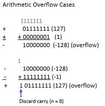
overflow can also occur when adding two negative values, which can result in a sum that exceeds the maximum negative value in the value range. Adding positive and negative values or adding negative and positive values will not exceed the maximum positive or negative value range in 2’s complement signed format. Understanding how to interpret the results of signed and unsigned arithmetic operations is important because digital systems are designed with a limited, fixed number of bits for number representation.
1.5 Binary Encoding Schemes
Digital systems interface with a variety of human interaction devices and applications using binary encoding schemes. A couple of examples of those schemes are presented here. Binary Coded Decimal (BCD) is an encoding scheme that represents the decimal values 0-9 for displays such as seven segment displays that are commonly used in household appliances, clocks, etc. The BCD scheme requires a 4-bit binary word to represent the 10 decimal digits 0-9 with words 0000-1001. The combinations 1010-1111 do not represent valid single digit decimal values, so are designated as not used.
BCD values may be used in operations such as addition. An example of adding the BCD values 8+6 is shown (right, top). From the example, adding decimal values 8+6 yields 14 which is 1110. This value is not a valid BCD combination. There are 6 binary combinations that are not valid BCD combinations for decimal values above 9. In order to translate a value above 9 into BCD format, add 6 to the value to remap the value into the BCD value range. Adding 6 creates a carry out of the most significant bit to yield two BCD values. For this example, adding 6 (0110) to 14 (1110) gives 0100 (4) with a carry out of 1. The BCD sum is 1 0100 for BCD values 1 4, which is the sum of 8+6 in decimal.
The second binary encoding scheme presented here is Gray code. Gray codes are commonly used for data encoding in electromechanical systems such as instrumentation and robotic positioning. The tip of a positioning sensor is shown in Fig. 13 (right, bottom). The analog sensor values correspond to a position in one of eight octants. Concentric circles partition the tip positioning with individual bits assigned to each region for labeling positions using octants with 3-bit
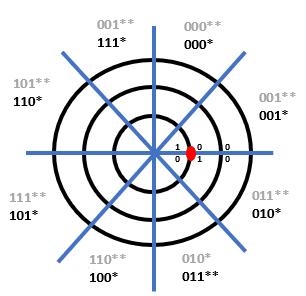
BCD Addition 8 1000 (BCD 8) +6 + 0110 (BCD 6) 14 1110 (if sum > 9, add 6) + 0110 ⌊1⌋ ⌊0100⌋ 1 4 BCD sum
code.
Fig. 1‐3. Binary coding positioning sensor example. *Incorrect code. ** Correct
combinations. Let the octants be labeled 000 (0), 001 (1), 010 (2), 011 (3), 100 (4), 101 (5), 110 (6), and 111 (7) going in a clockwise direction (given in black and denoted with *). Let the sensed value be represented as the red dot shown on the figure below. The sensed value is near bit boundaries where the binary combinations of the bit position may be encoded as 000, 001, 010, 011. The variations of the bit encoded combinations may differ by up to two bits (such as 001 and 010 OR 000 AND 011). With adjacent positions having labels that may differ by more than one bit, there may be discontinuities in the sensed positions. The possible encoded value of 011 is not in the actual 011 octant. Accordingly, an octant labeling scheme is needed with adjacent octant positions differing by a single bit.
Gray codes provide an example of such an encoding scheme. The rules to form Gray codes with any number of bits are:
1) 1-bit Gray code has two codewords: 0, 1
2) First 2n bits of n+1-bit Gray code are n-bit Gray codewords written in order appending a leading 0.
3) Last 2n bits of n+1-bit Gray code are n-bit Gray codewords written in reverse order appending a leading 1.
Applying these rules, the determined 1-bit, 2-bit, and 3-bit Gray codes are shown below. The Gray code labels assigned to each octant in the sensor positioning example are given in red. From the detected position represented as a dot in the senor positioning example, the bit boundaries give the possible labeled octant combinations of 001 and 011. These combinations differ by a single bit, allowing for adjacent positions to be maintained as valid labels for the actual detected position. The 3-bit Gray code labeling for the senor tip position example in Fig. 1-3 is shown denoted in gray with **. The use of Gray codes is also useful in the analysis of logic equations using Karnaugh maps, which will be examined in Chapter 3.
References
1Developed by Roger Younger at Missouri University of Science and Technology.
2https://exploreembedded.com/wiki/Analog_JoyStick_with_Arduino. Accessed May 12, 2022.
Gray codes 1 bit 2 bit 3 bit 0 0 0 0 0 0 1 0 1 0 0 1 1 0 0 1 0 1 1 0 1 1 1 1 1 1 1 0 1 0 1 1 0 0
Chapter 2: Boolean Algebra
Chapter 2 Learning Goals
Formulate logic expressions
Implement expressions using logic gates
Express and manipulate expressions using Boolean algebra
Chapter 2 Learning Objectives
Identify basic logic operations and associated logic symbols
Identify logic identities and algebraic laws
Determine logic functions and truth tables
Use Boolean algebra to write combinatorial functions
Simplify logic expressions using Boolean algebraic reduction
Identify complete logic sets
Draw logic diagrams from combinatorial functions
Find a function from the logic diagram
Identify integrated circuits associated with logic gates
Formulate logic functions for hardware implementation
2.1 Overview of Digital Circuits
Digital systems use a variety of inputs and outputs with digital components to perform required operations. The inputs, output, and operations conventionally use binary values represented electrically. Analog inputs are converted to binary values based on voltage ranges prescribed by the technology used in the digital components. The outputs of the digital components are binary values in voltage ranges for the prescribed digital component technology. Examples of digital component logic families include Resistor Transistor Logic (RTL), Transistor-Transistor (TTL) technology, Emitter Coupled Logic (ECL), and Complementary Metal on Oxide on Semiconductor (CMOS). Within each logic family, there are variations of IC implementations based on speed, power usage, power supply voltage, input/output voltage ranges for logical 0s and 1s, physical size, among others. The context of examining logic families in this textbook are to: 1) illustrate digital circuit implementation considerations and 2) highlight logic gate configuration.
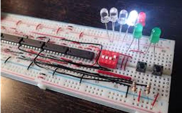
Fig. 2-1 above presents an example of a digital circuit. The circuit input is three switches (there are actually four switches, but only three are connected) with the output having seven light emitting diodes (LEDs) that are configured in a 7-segment display. The switch inputs, with a specific combination of the switch values as on or off, are connected (wired) to electrical components (ICs) to perform logical operations to generate logical outputs that turn on/off the individual LEDs to form the number 5 in the 7-segment display. This digital circuit is implemented on a prototyping platform called a breadboard. The breadboard has organized holes, called slots, where the pins of ICs may be inserted into the board. The column groups of five slots are electrically connected in
 Fig. 2‐1. Digital circuit implementation using a breadboard with digital components1
the breadboard so that wires and/or pins with the same logical or electrical value may be placed in the same column group. Also, notice that there are several (highlighted in yellow) column groups of two slots with red or blue horizontal bars across the breadboard. The horizontal bars are referred to as rails, with all slots in the same horizontal row sharing the same electrical value. Conventionally, the power supply value, typically 5 V, and the reference (also called ground), 0V, are connected (wired) from the power supply to the different rails to provide power and ground connection points for the circuit inputs, digital components, and outputs for the digital circuit. The purposes for this example are to: 1) highlight that the end goal of digital circuit design is prototyping and implementation, 2) provide the context for the design of digital circuits, 3) provide the context for the usage of digital components in digital circuits. The primary focus on this textbook is to develop an understanding of the theoretical, mathematical, and logical core concepts needed to design and apply digital components with specific operations for digital circuit design. Digital components, their functionality, utilization, and application in digital systems will be presented. Beginning in this section, the underlying digital logic is presented for digital components, logic operations, and logic expressions. The fundamental logic operations used in designing digital circuits and operations include the NOT (inverter), AND, OR, EXCLUSIVEOR, EXCLUSIVE-NOR, NAND, NOR. Logic operations utilize binary variables, which can take on the values 0 and 1. In digital systems, binary variables take on the form of analog inputs such as switches, buttons, window sensors, door sensors, etc. Analog inputs such as these have voltage ranges between the power supply value and the reference value, commonly referred to as ground. Voltage ranges, depending on the IC logic family technology, are translated into binary values that are interpreted as logical 0s and 1s. Digital circuits receive the analog voltages for the inputs, interpreted as 0s and 1s within the circuit, perform the logical operation within the circuit to generate an interpreted 0 or 1 logical output represented as an analog voltage. Combinations of one or more binary variables are used to express each logic operation. A truth table provides all input binary variable combinations with the associated output of the logic operation. The logic operations with truth tables and logic gate representations are presented in the next section. Other than the NOT operation, which has one input variable, all logic operations are introduced with two variable inputs.
2.2 Logic Operators
2.2.1 NOT Operator
Given a binary variable A that can take on the values 0 and 1. For the NOT operation:
�� 0, ��ℎ���� �� �� �� 1
As the notation shows, there are several operators that refer to the NOT operation. This textbook will primarily use the first two forms. In digital logic, the NOT operation is also referred as INVERT and COMPLEMENT. Inverting a variable means applying the NOT operation to the
����
variable. The truth table for the NOT operation with the input variable A, and the logic symbol for the NOT operation, more commonly referred as the inverter, are given as follows.
The bubble shown on the inverter is commonly used in digital logic to denote the NOT operation.
2.2.2 OR Operator
Using two binary variables (A,B), the logical OR operation is defined as:
and is expressed as A+B = AvB. The truth table for the two variable OR operation and the associated OR gate logic symbol are given below.
2.2.3 AND Operator
Using two binary variables (A,B), the logical AND operation is defined as:
1 and is expressed ��∙�� AB = A^B. The truth table for the AND operation and associated logic symbol are shown below.
1,
���� �� 1 ���� �� 1 ���� ������ℎ �� 1, �� 1, ��ℎ���� �� �� 1
���� ��
������ ��
��ℎ���� ��∙��
Truth Table A A’ 0 1 1 0 input output Truth Table A B A+B 0 0 0 0 1 1 1 0 1 1 1 1 Truth Table A B A∙B 0 0 0 0 1 0 1 0 0 1 1 1 A ’ Inverter A AB B AND Gate A A+B B OR Gate
1
Using AND, OR, and INVERT gates, any arbitrary logic network or function can be implemented. Any combination of logic gates that can implement any arbitrary logic function is referred to as a complete logic set
2.2.4 NAND Operator
There are additional logic gates that are commonly used to implement logic functions in digital circuits. The NAND operation is interpreted as NOT-AND, which is expressed as:
The truth table and associated logic symbol for NAND are given as:
2.2.5 NOR Operator
The NOR operation is interpreted as NOT-OR, which is logically expressed as:
The truth table and associated logic symbol for two input NOR operation are:
2.2.6 Exclusive‐OR (XOR)
The Exclusive-OR (XOR) operation is interpreted for the two-variable case as:
if A = 1 OR B = 1 but not both, then the XOR is 1.
Logically, the XOR operation is shown as: A⨁B. The truth table and gate symbol for the XOR gate are given below.
��∙��
���� ���� ′
�� �� = (A +
B)’
A B A B �� ∙�� 0 0 0 1 0 1 0 1 1 0 0 1 1 1 1 0 A B �� �� �� �� 0 0 0 1 0 1 1 0 1 0 1 0 1 1 1 0 A ���� B NAND Gate A �� �� B NOR Gate
All of the logic operators presented to this point, except for the inverter, have been shown with two inputs. The OR, AND, NAND, NOR, and XOR gates have more than two input IC components available. Consider the XOR gate with three inputs ABC. Its truth is shown below. In order to find the XOR gate outputs for each combination of ABC, the outputs for the two input A and B XOR are found for all combinations of ABC (truth table shown to the left). Since C does not affect the XOR of AB, the XOR entries for AB are the same for both C = 0 and C = 1. After finding ��⨁�� , the ��⨁�� entries are determined with the associated input values of C (XOR the column entries with the downward arrows shown on the truth table). Inspecting the truth table entries for ��⨁��⨁�� , ��⨁��⨁�� is 1 whenever the combination of input variables ABC with a 1 value is an odd number. The ABC input combination entries in the truth table with an odd number of variables with 1 values are highlighted with left-pointing arrows by the truth table (with the total number of 1 values for ABC). Thus, the XOR is an odd function. If you had an XOR gate with 20 input variables and an odd number of those variables are 1s, the output of the XOR gate is 1.
2.2.7 Exclusive‐NOR (XNOR) Operator
The Exclusive NOR operation is NOT-Exclusive OR, denoted as XNOR. The logical operator for the XNOR gate is given as A⨁B ��⊙�� . The truth table for the XNOR gate is shown below. Since the XOR operator is an odd function and the XOR operator is the complement of the XNOR operator, the XNOR operator outputs a 1 whenever there are an even number of input variables with 1 values. Thus, the XNOR is an even function.
Truth Table A B A⨁B 0 0 0 0 1 0 1 0 0 1 1 1 A B C ��⨁�� ��⨁��⨁�� 0 0 0 0 0 0 0 1 0 1 0 1 0 1 1 0 1 1 1 0 1 0 0 1 1 1 0 1 1 0 1 1 0 0 0 1 1 1 0 1 A ��⨁�� B XOR Gate
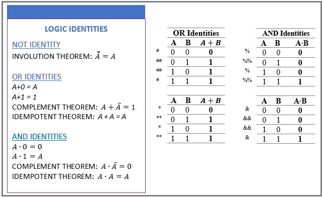
2.3 Logic Identities and Algebraic Laws
In this section, logic identities are presented to utilize logic gates for designing and implementing digital circuits. The Logic Identities provide the basis to manipulate individual logic variables (shown in Fig. 2-2 below). The involution theorem logically shows the application of the NOT operator to a logic variable. Let A = 0. By the involution theorem, 0 1 0. For the OR identities, consider the truth tables for the OR operation (OR Identities in Fig. 2-2). Let B = 0. A + 0 = A (denote as *), and A+1 = 1 (**). From the right truth table, the idempotent theorem A + A = A (#), and the complement theorem �� �� 1 (##). For the OR identities, consider the truth tables for the AND operation (AND Identities right). Let B = 0. From the left truth table, A ∙ 0 = 0 (%), and ��∙ 1 = A (%%). From the right truth table, the idempotent theorem ��∙�� �� (&), and the complement theorem ��∙�� 0 && .
A B A⨁B ��⨁�� 0 0 0 1 0 1 0 1 1 0 0 1 1 1 1 0 A ��⨁�� B XNOR Gate
Fig. 2‐2. NOT, OR, and logic identities with truth table verification.
Fig. 2-3 (above) presents Commutative, Associative, and Distributive algebraic laws with the precedence of logic operations that are used to represent logic functions. The Commutative Law provides for logic variables and terms to be placed in different positions within logic expressions without impacting the logical equivalence of the expression. The Associative Law gives the order of logic operations to represent and evaluate logic expressions. The core three logic operators are NOT, AND, and OR. NOT has the highest logic precedence. The AND operator has a higher precedence than OR. Logic expressions in parentheses are evaluated first in following the precedence of operators. From the algebraic laws, Fig. 2-4 (below) shows three logic function examples to show the order of operations to evaluate each function.
 Fig. 2‐3. Algebraic Laws used for expressing and manipulating logic functions.
Order Operations are performed F = X (Y+Z) F = A’B + CD F = (A’B)’ + CD 1 Y+Z A’ A’ 2 X (Y+Z) A’B CD (Concurrent) A’B 3 A’B + CD (A’B)’ 4 CD 5 (A’B)’+CD
Fig. 2‐4. Examples applying precedence of operations to evaluate logic functions.
There are two forms of the distributive law to formulate logic functions based on combining variables using parentheses. The distributive law A (B + C) = A B + A C is an intuitively mathematical combination and expansion of terms. The distributive law A + B C = (A + B) (A + C) is less intuitive but logically ORs the isolated variable (A) with each variable in the other term (B C), ANDing the resulting terms. Fig. 2-5 gives a couple of examples applying this distributive rule.
Distributive Law Examples
2.4 DeMorgan’s Theorems
Two additional Boolean algebra tools for manipulating logic expressions are DeMorgan’s theorems, which are stated as: 1)
DeMorgan’s theorems relate NOR with AND NAND with OR operations. The truth tables for each DeMorgan’s theorem are shown in Fig. 2-6 below to verify the logical equalities.
For each DeMorgan’s theorem, break the NOT (line) between the variables through the OR AND operator, then replace the OR with an AND or operator, respectively, and keep the NOT with each variable on each side of the replaced operator.
Fig. 2‐5. Examples manipulating a logic function using the distributive rule.
�� �� �� ∙��
��∙�� �� ��
2)
Fig. 2‐6. Truth table verification for DeMorgan’s theorems.
A + B C = (A + B) (A + C) F + W’ X Y’ Z = (F + W’) (F + X) (F + Y’) (F + Z) �� �� �� ∙�� A B �� �� �� �� �� ∙�� 0 0 1 1 1 1 0 1 0 1 0 0 1 0 0 0 1 0 1 1 0 0 0 0 �� ∙�� �� �� A B �� ∙�� �� �� �� �� 0 0 1 1 1 1 0 1 1 1 0 1 1 0 1 0 1 1 1 1 0 0 0 0
2.5 Logic Functions and Networks
Using these logic operations, identities, algebraic laws, and theorems, examples of finding a logic function from a truth table, finding a truth table from a logic function, and drawing a logic circuit (logic network) from a logic function are presented. A logic function or logic expression utilize combinations of logic operations with binary variables.
To find a logic function from a truth table, consider the truth table example in Fig. 2-7 above. There are three input variables A, B, and C with output F, with 0 and 1 entries arbitrarily chosen for this example. With three input variables, there are 23 = 8 rows in the truth table, with decimal equivalents of 0 (ABC = 000) to 7 (ABC = 111). Applying the logic identities to each 1 output (F) entry, the combination of variables A, B, and C are found to create a logical 1 term. The F = 1 entry for ABC = 000 can be phrased as an if-then rule, namely: if A = 0 AND B = 0 AND C = 0, then F = 1. Translating this if statement to a logical term is done by making each variable form as a logic 1 value ANDing the variable forms to create the logical term. In this case, to express A = 0 as a logical 1, use A’, which translates as 0’ = 1. The same is true for B = 0 and C = 0 to give the forms B’ and C’. From the logic identity X 1 = X, ANDing the variable combinations A’B’C’ = 0’ AND 0’ AND 0’ = 1 AND 1 AND 1 = 1 to yield F = 1. This process is repeated for all F = 1 entries in the truth table. The individual terms are found for all of the 1s entries. The logic function F is obtained using the logic identity 1 + X = 1 to logically OR all of the individual terms formed from the 1s entries in the truth tables. For this truth table example, there are four 1s entries for F, giving F = A’B’C’ + A’BC + AB’C’ + ABC as the resulting logic function. If the any of the input logic variable combinations is satisfied, then the term in F is a logic 1. The logic identity 1+X = 1 means that if any of the terms is a logic 1, then F = 1.
Fig. 2‐7. Example of finding a function from a truth table.
a logic
a truth table A B C 0 0 0 IF A = 0 AND B = 0 AND C = 0, �� ∙�� ∙�� 0 ∙ 0 ∙ 0 1 0 0 1 0 1 0 0 1 1 IF A = 0 AND B = 1 AND C = 1, �� ∙��∙�� 0 ∙ 1 ∙ 1 1 1 0 0 IF A = 1 AND B = 0 AND C = 0, �� ∙�� ∙�� 1 0 0 1 1 0 1 1 1 0 1 1 1 IF A = 1 AND B = 1 AND C = 1, �� ∙��∙�� 1 1 1 1 Using the OR identity X + 1 = 1, the logic function �� �� ���� �� ���� ������ ������
Find
function from
In order to find the truth table for F in the example (Fig. 2-8), the truth table for the individual terms can be found, logically ORing the truth tables from each term using the identity 1+X =1 to give the truth table for F. For the first term A’B, A = 0 to give A’ = 0’ = 1 with B = 1 for A’B = 0’ AND 1 = 1 AND 1 = 1. Finding the truth table for A’B, the if-then rule: if A = 0 AND B = 1, the truth table entries are 1s (0s otherwise). Note, the term only depends on the values of A and B. The value of C does not matter to satisfy the if then rule in determining the truth table entries. A similar process is applied for finding the truth tables for the other terms AC and BC’. Once the truth table entries are found for all of the terms (denoted with arrows), then the truth table for F is found by ORing the truth table entries for those terms using the identity 1+X=1.
Determine the logic network (digital circuit) for �� ���� ���� ����
In the next example (Fig. 2-9 above), a logic network (digital circuit) is determined for a given function f. In the logic network implementation, the symbols for the logic gates are substituted for each logic operation. A’ is replaced by placing a wire from the variable A to the input of an inverter. The output of the inverter is A’. The term A’B is formed taking a wire from the output of the inverter (A’) to the input of a 2-input AND gate with a wire from the variable B. The output of this AND gate is A’B. For the second term, AC, wires are drawn from the variable A to the 2input AND gate. Since a wire has already been drawn from the variable A, a solder point is made on the existing wire for A and the wire is drawn to the input of the 2-input AND gate. This solder point indicates that the wires are connected. A similar process is performed to generate the term BC’. For combining the individual terms, 2-input OR gates are shown with wires from the outputs
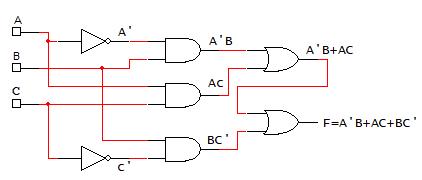 Fig. 2‐9. Example of drawing the logic network from a function.
Find the truth table for �� ���� ���� ���� A B C 0 0 0 0 0 1 0 1 0 0 1 1 1 0 0 1 0 1 1 1 0 1 1 1
Fig. 2‐8. Example of finding a truth table from a function.
of two of the AND terms as inputs to an OR gate. The output of the this OR gate has a wire drawn as an input to a second OR gate with the remaining AND gate output, with F as the output of the OR gate. Note that many gates can be expressed using with more than 2 inputs. In the example above, a 3-input OR gate could have been used to take the wires from the three AND gates to produce the function output f.
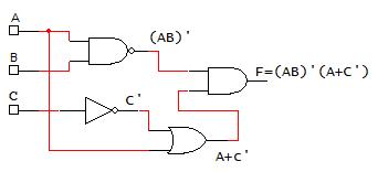
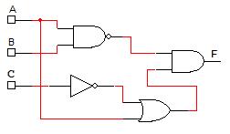
In next example (Fig. 2-10 below), the logic expression and truth table are determined from the logic network (digital circuit), there are 3 input variables (ABC) and one output (F). In order to determine the logic function from the logic network, work from the logic network inputs to put together the individual terms from the logic gates going from left-to-right. The term from the output of each logic gate is used as an input to the next logic gate in the logic network until the output of the logic gate is F. The truth table for F can most easily be obtained by finding the truth table for the individual terms and combining the terms. In this case, there are two terms (AB)’ and (A+C’). The truth tables for those terms can be found and combined with AND operation (since these terms are ANDed to yield F).
Determine the logic function and truth table from the given logic network.
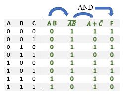
Logic
Truth Table
Logic Network
Function
Fig 2‐10. Example of finding a logic function and truth table from a logic network.
2.6 Digital Circuit Implementation
In the previous sections, binary variables, logic operators, logic identities, and algebraic laws were introduced to represent and interpret logic functions. The manipulation of logic functions using these logical and algebraic operations is referred to as Boolean algebra. The goal of obtaining and manipulating logic functions is to put the logic function into a form that can be implemented using hardware components. TTL components were introduced for the different logic operators.

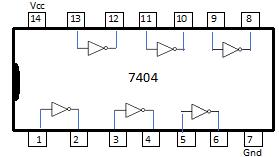
For digital circuit implementation purposes and examples presented in future chapters, each logic operator is referenced by a TTL part. The TTL 7404 is the digital component for the inverter (see Fig. 2-11 below). The 7404 is a standard part with many manufacturers. An example of the datasheet for the 74LS04 is given at http://pdf.datasheetcatalog.com/datasheets/70/375318_DS.pdf. The 74LS04 is one of the variants that uses a low power Schottky (LS) transistor in the inverter physical component implementation. This IC is a commonly used variant in the physical breadboard implementation of digital circuits. The datasheets for ICs can be found at websites such as www.datasheetcatalog.com and www.digikey.com. The IC, in this case, is a dual inline package (DIP). The schematic is called a pinout diagram. The pinout diagram shows that there are six inverters on a single IC, with power (Vcc) and ground (Gnd) for powering the IC. An example of the TTL 7404 IC is shown in Fig. 2-12 below with a picture of the IC used in a breadboarded circuit labeled with a yellow arrow. The datasheet provides details such as the power supply voltage (Vcc), the voltage levels for the input and output variable(s), the electric current ratings or operating conditions for the IC, the timing or speed for transitioning the input value to the associated output value (typically on the order of nanoseconds), the temperature range for using the IC, and the physical dimensions of the IC. For TTL technology, the standard power supply is 5V. The six inverters work identically and may be use in any order.
33
Vcc 14 13 12 11 10 9 8 1 2 3 4 5 6 7 Gnd
Fig. 2‐11. TTL 7404 (Inverter) IC and pinout diagram.
A table is shown below in Fig. 2-13 presenting the standard TTL ICs for the logic gates presented in the previous sections. The TTL parts provide a practical example of wiring the connections to generate and combine the terms in the function to generate the function. Conventionally, the binary variable inputs are given as switches, and the output of the function is displayed using a light emitting diode (LED). For wiring the connections in the breadboard implementation, datasheets are needed for each IC (also referred to as a digital component).
The datasheets provide details about using the ICs, including voltage, current, and temperature requirements, as well as physical IC implementation details with a pinout diagram. The pinout diagram shows the usage for each pin, including power and reference (ground) and the input(s) and output(s) for each logic gate. Datasheets can be obtained for digital components from the manufacturer’s website or from common websites such as http://datasheetcatalog.com and http://digikey.com. An example of a logic function implementation with the wiring connections such as would be done on a breadboard is presented in Fig. 2.14. The pin numbers on the different ICs are shown with each gate.
34
Fig. 2‐12. Digital circuit implemented using ICs and LEDs on a breadboard. A TTL 7404 IC is labeled with a yellow arrow.
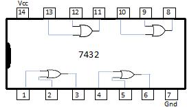
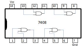
Logic Gate TTL Part Number Number of Gates on IC Inverter (NOT) 7404 6 AND (2‐Input) 7408 4 OR (2‐Input) 7432 4 NAND (2‐Input) 7400 4 NOR (2‐Input) 7402 4 XOR (2‐Input) 7486 4
Fig. 2‐13. Standard logic gates with the TTL part number and the number of gates on the associated ICs.
Determine the logic network (digital circuit) for
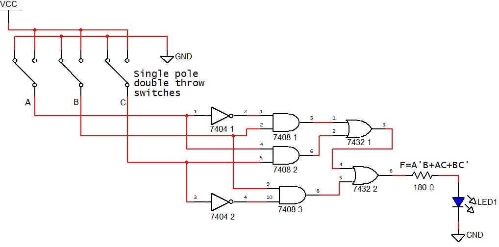
IC Part/Number of gates
7404 (Inverter)/2
7408 (2‐input AND)/3
7432 (2‐input OR)/2
35
�� ���� ���� ����
Fig. 2‐14. Logic function implementation using TTL logic gates with corresponding IC wiring diagram.
A B C f
2.7 Design Problem Word Problems
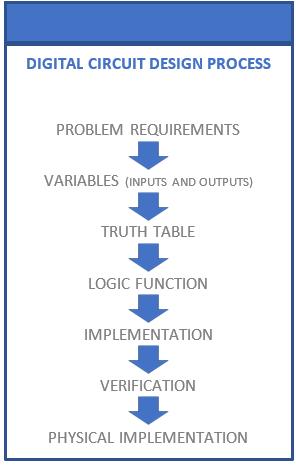
The digital circuit design process (Fig. 2-15) begins with a problem statement to specify the problem. From the problem specification, the design requirements are identified. Binary input and output variables are determined with the associated interpretations of logic 1 and 0 values for each variable. Using the problem requirements and input and output variable designations, truth table is found. From the truth table, a logic function is derived. Based on the problem requirements, the logic function is implemented using logic gates or other digital components (presented in Chapter 5). Conventionally, digital circuit design tools are used to simulate the logic function implementation for truth table verification. Then, the simulated logic function implementation is translated to a physical circuit implementation such as a breadboard. We will explore the various steps in the digital circuit design process throughout this and remaining chapters of the textbook, beginning with the problem statement and requirements in the next section.
36
Fig. 2‐15. Digital design process.
Figs. 2-16 and 2-17 present examples of the digital circuit design process to determine problem variables and the associated truth table.
Design Problem Example: Fire Sprinkler System
Problem Requirements: A fire sprinkler system should spray water if the heat sensor is sensed and the system is set to be enabled.
Identify Variables
Input variables: h = heat sensor (high heat is sensed)
Specify values: 0 = no high sensed heat, 1 = high sensed heat
E = system enable
Specify values: 0 = system not enabled, 1 = system enabled
Output variable: f = turning on/off sprinkler system
Specify values: 0 = sprinkler system off, 1 = sprinkler system on
Find the Truth Table
Apply problem requirements with input and output variables to determine the truth table: A fire sprinkler system (f) should spray water if the heat sensor is sensed AND the system is set to be enabled
37
Fig. 2‐16. Fire sprinkler design problem example.
IF h = 1 AND E= 1, THEN f = 1 h E f 0 0 0 0 1 0 1 0 0 1 1 1
Design Problem Example: Car Alarm System
Problem Requirements: A car alarm system should sound if the alarm is enabled and either the car is shaken or the door is open.
Identify Variables
Input variables: s = door is shaken
Specify values: 0 = door is not shaken, 1 = door is shaken
d = door is open
Specify values: 0 = door is open, 1 = door is closed
e = system is enabled
Specify values: 0 = system is not enabled, 1 = system is enabled
Output variable: f = car alarm sound activation
Specify values: 0 = not activated, 1 = activated
Find the Truth Table
A car alarm system should sound if the alarm is enabled AND either the car is shaken OR the door is open.
IF e = 1 AND s = 1, THEN f = 1
IF e = 1 AND d = 0, THEN f =1
OTHERWISE, f = 0
e = 0 (system not enabled)
38
Fig. 2‐17. Car alarm design problem example.
e d s f
= 1 AND d
0 e = 1 AND s = 1 0 0 0 0 0 0 1 0 0 1 0 0 0 1 1 0 1 0 0 0 1 0 1 1 1 1 0 0 1 1 1 1
e
=
2.8 Logic Function Simplification Using Boolean Algebra
There are a variety of considerations in implementing logic functions. In the previous section, logic function implementation was illustrated using a breadboard with TTL components. This example highlights some of the considerations such as the size of the implemented circuit in terms of the number of components used and the number of logic gates on those components. Much of digital logic explores different types of digital components that can utilized to implement logic functions and perform logic and arithmetic operations. This book presents a number of those digital components with the context of their application and utilization in digital circuit implementation.
Logic gates and identities and algebraic laws have been introduced to implement logic functions. The goals of digital circuit implementation are:
1) Minimize the number of digital components to reduce the power requirements and size of the digital circuit.
2) Configure the logic function in a form that meets the speed or timing requirements for the application using the logic function. For different logic families (TTL, CMOS, etc.), variations of digital components are often available that are fabricated with enhanced speed and reduced power to promote digital circuit implementation to meet a variety of application requirements. In addition, reducing the complexity of the logic functions contributes to satisfying goals 1 and 2.
3) Manipulating the logic function for implementation using specified logic operations or digital components. In some cases, manipulating a logic function for implementation using specific logic operations may contribute to meeting goals 1 and 2.
In this section, logic function simplification is examined using Boolean algebra to facilitate meeting digital circuit implementation goals. The truth table can be used to verify the equality of logic expressions, as shown in the verification of the DeMorgan’s theorems. Logic expressions can be manipulated for simplification and to put expressions in different forms for implementation. For simplification, logic functions are manipulated to eliminate redundancies. A logic expression redundancy is where one or more variables or terms contributes nothing unique to the logical equivalency (same truth table for the function with or without those variables or terms). Fig. 2-18 gives a summary of the logic identities for manipulating expressions using Boolean algebra.
39
OR‐based AND‐based
A + 0 = A �� ��
A + 1 = 1 A ∙ 0 = 0
A + A = A ∙ 1 = A
�� �� 1 ��∙�� 0
A + B = B + A AB = BA
A + B + C = (A + B) + C ABC = (AB)C
A(B + C) = AB + AC A + BC = (A + B)(A + C) ���� �� �� ��
Fig. 2-19 through Fig. 2.25 present Boolean expression simplification examples to eliminate redundancies. The context of logic expression simplification based on the logic gates and digital components required for Boolean expression implementation are also shown.
Simplify the expression using Boolean algebra into the simplest form.
g = xyz + xz Logic gates needed to implement (before simplification)
3 2‐input AND gates (7408) needed: [xy] [(xy)z] [xz]
1 2‐input OR gate (7432) needed: [(xy)z] + [xz]
2 parts (1 7408 IC and 1 7432 IC) using 4 total gates
Simplification steps
g = xyz + xz
g = (xz) (y + 1) Distributive Rule AND A 1=A AND Commutative Rule (ABC = CAB)
g = (xz) (1)
1+A = 1
g = xz A∙1 = A
Simplest form
g = xz Logic gates needed to implement (after simplification)
1 2‐input AND gate (7408) needed: xz
1 part (1 7408 IC) using 1 gate
40
Fig. 2‐18. Summary of Boolean algebra logic identities and algebraic laws.
Fig. 2‐19. Boolean algebra logic simplification example.
Identities and Algebraic Laws
�� �� ��
Example 1: Boolean algebra and reduction
From Fig. 2-19, the unsimplified function g = xyz + xz requires three 2-input AND gates (TTL component 7408) and one 2-input OR gate (TTL component 7432), which means that breadboarding the function g has 2 TTL digital components. In the reduction/logic simplification process for this function, the identities applied are given for each step. The simplification process is completed when no additional identities can be applied to eliminate any redundancies. The simplified function g = xz requires one 2-input AND gate. The simplification process here eliminates three logic gates and one TTL component, resulting in the breadboard implementation only using one TTL 7408 2-input AND gate component.
Let X = A+B is common in both terms so use X to substitute in h h = (X+C)(X) Substitute X in h
= XX + XC
= X + XC
Distributive Rule (L (M+N) = LM + LN)
From Fig. 2-20, the logic function h has two ANDed terms with ORed forms of the variables. In this case, the two terms have A+B in common. Substituting X = A+B in the function h makes the simplification process simpler. Applying the logic identities to simplify h is done until redundancies are eliminated. Then, A+B=X is substituted to get the final functional form.
41
Fig. 2‐20. Boolean algebra logic simplification example.
Example 2: Boolean algebra logic function simplification for h = (A+B+C)(A+B)
L∙L = L
Distributive
= X (1) 1+L = 1 = X L∙1 = L
A + B Substitution X = A+B Simplest form
= X (1 + C)
Rule (L (M+N) = LM + LN)
=
Example 3: Boolean algebra logic function simplification (Proof Distributive Rule)
Show A + BC = (A+B) (A+C)
Steps
(A+B) (A+C) = AA + AC + AB + BC
Logic Identity or Algebraic Law
Distributive rule (A (B+C) = AB + AC), Communitive Rule XY = YX
= A + AC + AB + BC X∙X = X (Idempotent theorem‐AND)
= A (1 + C + B) + BC
= A (1) + BC
Distributive rule (A (B+C) = AB + AC)
1+X = 1
= A + BC X 1 = X
Proof of equality
The example in Fig. 2-21 is a proof of the distributive rule form with A+BC = (A+B)(A+C). The important step to note in the simplification process is taking A+AC+AB+BC = A(1)+AC+AB+BC. Then, A(1)+AC+AB+BC = A(1+C+B). Using A=A(A) instead of A=A(1) results in A+AC+AB+BC = A(A+C+B)+BC. The term A+C+B does not simplify any further. In applying this distributive rule the term A+BC is given as ORing the isolated variable A with each variable in the other term, ANDing each ORed term generated. In this case, A is ORed with B to give (A+B), and A is ORed with C to give (A+C). The two ORed terms are ANDed to yield the distributive rule form, which is (A+B)(A+C). This distributive rule is very useful in simplifying Boolean expressions, especially as a last resort when no other identities can be applied.
The example in Fig. 2-22 (below) presents two approaches to simplify the function. Approach 1 illustrates the use of the distributive rule (from example 3) for simplification. X+X’Y’ contains an isolated variable (X) with the other term having the complement of that variable (X’). The distributive rule is applied by ORing X with each variable in its form in the other term, ANDing the resulting terms, giving (X+X’)(X+Y). X+X’ = 1, eliminating this term. So, X+X’Y’ = X+Y’. Applying distributive rule in this condition effectively eliminates the complement of the variable in the other term.
In approach 2, the terms in the unsimplified expression are examined for commonalities. XY’ has a common X with the term XY, and XY’ has a common Y’ with the term X’Y’. With XY’ having commonalities with other terms, creating an extra copy of XY’ can be used to simplify each of those other terms. Since A+A=A, the extra copy of XY’ maintains the equality of the expression (XY’ + XY’ = XY’). Adding the copy of XY’ allows XY’ to be paired with the other terms to simplify the expression.
42
Fig. 2‐21. Boolean algebra logic simplification example.
Example 4: Boolean algebra logic function simplification (Proof)
Show XY + XY’ + X’Y’ = X + Y’ using 2 approaches:
Proof
Simplify
Example 5: Boolean algebra logic function simplification
43
Fig. 2‐22. Boolean algebra logic simplification example.
Fig. 2‐23. Boolean algebra logic simplification example.
XY + XY’ + X’Y’ = X(Y + Y’)
X’Y’ Dist. Rule = XY + XY’ + XY’ + X’Y’ A+A = A = X(1) + X’Y’ A+A’ = 1 = X(Y+Y’) + Y’(X+X’) Dist. Rule = X + X’Y’ A∙1 = A = X(1) + Y’(1) A+A’ = 1 = (X + X’)(X + Y’) Dist. Rule (A+BC = (A+B)(A+C) = X + Y’ A∙1 = A = (1)(X + Y’) A+A’ = 1 Proof of equality = X
A∙1 = A
Approach 1 Approach 2 XY + XY’ + X’Y’
+
+ Y’
of equality
�� �� �� �� �� ��
Approach 1 Approach 2 �� �� �� �� �� �� �� �� �� �� = �� �� �� �� �� �� �� �� Dist. Rule = �� �� �� �� �� DeMorgan’s theorem = �� �� �� �� �� �� �� A A = A �� �� �� �� = �� 1 �� �� �� �� Dist. Rule = �� �� �� �� �� DeMorgan’s theorem = �� �� �� 1+A = 1, A 1 = A �� �� �� �� = �� �� �� DeMorgan’s theorem = �� �� �� �� �� �� �� �� �� �� �� = �� �� �� �� Dist. Rule = �� �� �� �� �� = �� �� �� �� �� Dist. Rule = �� �� �� DeMorgan’s theorem A+BC = (A+B)(A+C) �� �� �� �� = �� �� �� �� �� 1 = �� �� �� * �� �� = �� �� �� * Commutative Law = �� �� �� �� * Dist. Rule = �� �� �� �� * Dist. Rule Simplest form* Simplest form*
2 approaches are presented:
From Fig. 2-23 (above), the logic expression (g) is to be simplified in a form that uses the fewest number of logic gates, excluding inverters. There is no restriction on the number of inputs to the logic gates in the simplified form using the fewest number of logic gates. Two solutions are presented here. In approach 1, the terms under the NOT bar are expanded using the distributive rule, and then the identities are used to simplify the expression. There are multiple forms in simplifying the expression that use two logic gates, namely a(b’c)’ and a(b+c’). Eliminating the redundancies from g also provides the simplified form ab+ac’, which uses three logic gates (two AND gates, one OR gate), which does not provide the implementation that uses the fewest number of logic gates. There is a difference between simplifying the logic function that eliminates redundancies and the form of the simplified function that uses the fewest number of logic gates. If the goal of this problem is to find the simplest form of the function g, a(b+c’) or ab+ac’ are valid solutions.
In approach 2, g is treated as a NAND expression using DeMorgan’s theorem to represent and combine the individual NAND terms. The resulting expression is simplified using the identities. Using this approach, there is only one form of the simplified expression that uses two logic gates (a(c’+b)), and two forms of the expression that yield the simplified forms (a(c’+b) or ac’+ab).
Eliminate complement of isolated variable
in term �������� (see yellow term highlight for example variable elimination)
The example presented in Fig. 2-24 is more complex than the previous examples, utilizing multiple applications of the distributive rule in finding the functional simplified form. In the intermediate
44
Fig. 2‐24. Boolean algebra logic simplification example.
Simplify �� �������� ������ ���� ���� ���� �������� ������ ���� ���� ���� = �������� ������ �� �� �� �� Dist. Rule = �������� ������ �� �� �� 1, ��∙ 1 �� = �������� �� �� �� �� �� �� Dist. Rule (A + BC = (A+B)(A+C)) = �������� �� �� �� �� �� �� 1, ��∙ 1 �� = �������� ���� ���� ���� �� Dist. Rule, ��∙�� �� = �������� ���� �� �� �� 1 Dist. Rule = �������� ���� �� �� �� 1, ��∙ 1 �� = ������ ���� �� Dist. Rule (A +
Example 6: Boolean algebra logic function simplification
BC = (A+B)(A+C)) Simplified form
��
form of the expression w’x’z+y’+wx, wx is NOT the complement of w’x’; rather, wx is the complement of (wx)’ or (w’+x’). So, the distributive rule cannot be applied using those terms.
c is common to both terms
The example in Fig. 2-25 uses substitution for common groups of terms in the expression to aid in the simplification process. Without substitution, the terms are expanded to simplify the expression (what is done above is a simpler expression than without substitution).
2.9 Complete Logic Sets
Implementing logic functions utilizes combinations of logic gates. A combination of logic gates that can be used to implement any arbitrary logic function, which consists of the AND, OR, and NOT operations, is referred to a complete logic set. AND, OR, and NOT (inverter) gates constitute a basic complete logic set. Implementing logic functions using this combination of gates is referred to as using AOI logic. Examples of complete logic sets include:
45
Fig. 2‐25. Boolean algebra logic simplification example.
1) AND, OR, INVERT (AOI)
2) AND, INVERT 3) OR, INVERT 4) NAND-ONLY 5) NOR-ONLY
�� �� �� �� �� �� �� �� �� �� �� �� �� �� �� �� ��
x = a + b + c a + b
= �� �� �� �� Substitution = �� ���� ���� ���� Dist. Rule, ��∙�� �� = �� 1 �� �� ���� Dist. Rule = �� ���� �� �� 1, �� 1 1 = �� ��∙�� 0, �� 0 �� = �� �� �� Substitution Simplified form
Example 7: Boolean algebra logic function simplification
Simplify
Let
+
DeMorgan’s theorems provide the basis to showing that complete logic sets 2-5 can be used to implement AND, OR, and NOT operations necessary to implement any logic function. The following sections show how NAND-only logic and NOR-only logic are separately complete logic sets and how to implement functions using only these gates.
2.9.1 NAND‐BASED Logic
For NAND-based logic, logic functions are implemented using only NAND gates (different numbers of NAND gate inputs may be used in this approach). As previously state, NAND-based logic relies on the ability to implement AND, OR, and NOT operations using only combinations of NAND gates. The truth table and NAND gate manipulations to perform these operations are shown in Fig. 2-26 below.
NAND‐Only implementations of AND, OR, and NOT Operations
The following steps provide the process to implement a logic function using only NAND gates:
1) Draw the logic function using AOI logic, i.e. with AND, OR, and NOT (inverters) gates.
2) Substitute the NAND gate only combinations for each AND, OR, and NOT gates in the AOI implementation (as shown above).
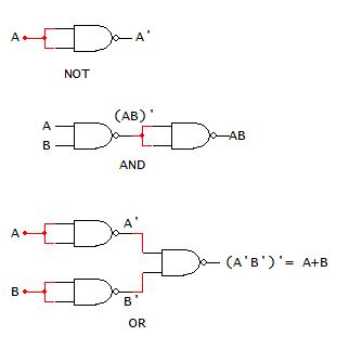
3) Eliminating redundant gates, specifically double NAND-based inverters from the circuit from step 2.
4) Determine the logic function for the NAND only implementation of the logic function to verify truth table equivalence to the original logic function from step 1.
46
Fig. 2‐26. NAND‐Only representations for AND, OR, and NOT operations.
A B �� ∙�� �� ∙�� 0 0 0 1 0 1 0 1 1 0 0 1 1 1 1 0 �� ∙�� �� �� �� �� �� ∙��
An example of implementing a function using NAND-only gates is presented in Fig. 2-27. As a consideration for implementation, the number of TTL components required to breadboard this function is shown in the AOI implementation.
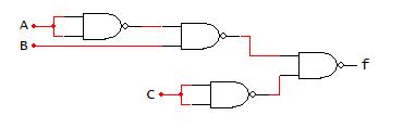
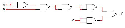
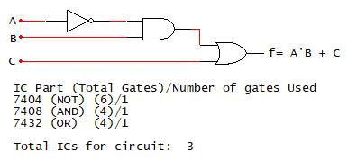
Implement �� ���� �� using NAND‐only logic
Draw f using AOI
NAND Gate Substitutions
Remove Double Inverters
Functional Equivalency:
47
�� ���� �� ���� �� ���� �� √
NOT AND OR
Fig. 2‐27. Example of NAND‐only logic gate implementation.
From Fig. 2-27, the AOI implementation of the function f requires three TTL components, using one NOT, AND, and OR gate on each of the components. Performing gate substitutions and eliminating NAND double inverter redundancies yields the function f = ((a’b)’c’)’, which is shown as equivalent to f = a’b+c. The NAND-only implementation requires four 2-input NAND gates, which is the number of 2-input NAND gates present on the TTL 7400 component. Thus, the function f can be implemented using only one TTL component compared to three TTL components using an AOI implementation. Accordingly, the NAND-only implementation provides the basis to reduce the size and power necessary to physically implement this circuit.
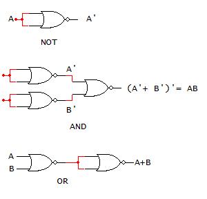
2.9.2 NOR‐BASED LOGIC
NOR-based logic is similar to the NAND-based logic only utilizing NOR gates to implement logic functions. The application of NOR-based logic to logic function manipulation requires determining combinations of NOR gates to represent the NOT, AND, and OR operations. If this cannot be done, then NOR-based logic does not represent a complete logic set. The truth table, DeMorgan’s theorem derivations, and NOR gate combinations to implement NOT, AND, and OR operations are shown in Fig. 2-28 below. The process for representing a logic function using a NOR-only representation includes the same steps as the NAND-only form. The gate substitution process is illustrated for the function f = a’b + c in Fig. 2-29 below.
48
NOR‐Only implementations of AND, OR, and NOT Operations
A B �� �� �� �� 0 0 1 0 0 1 1 0 1 0 1 0 1 1 0 1 �� ∙�� �� �� �� �� �� ∙��
Fig. 2‐28. NOR‐Only implementations of AND, OR, and NOT Operations.
Remove Double Inverters
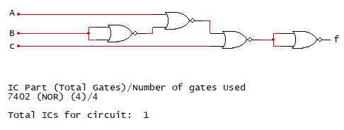
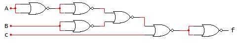
49 Implement �� ���� �� using NOR‐only logic
f using AOI
Draw
NOR Gate Substitutions
Functional Equivalency: �� �� �� �� �� �� �� ���� �� √
implementation. NOT AND OR
Fig. 2‐29. Example of NOR‐only logic gate
As shown in the NAND-only implementation example, the AOI implementation for f requires three TTL parts, which is the same in this example. Performing the NOR-only gate substitutions for the NOT, AND, and OR gates from the AOI circuit and eliminating the double inverter redundancies. The resulting NOR-only form of the function is f = ((a+b’)’+c)’’, which is shown to equal f = a’b+c. Using the NOR-only 2-input gate representation, four NOR gates are needed to implement f. Since there are four 2-input NOR gates on a single 7402 TTL component, one 7402 component is needed to implement f.
The example function f = a’b + c implemented using NAND- and NOR-logic representations illustrates two approaches that can be utilized to simplify and reduce the TTL components needed to implement f. The goal of using Boolean algebra and techniques such as NAND- and NOR-only representations is to develop a toolbox that logic function implementation can be manipulated to address size/space, power, parts available, among other considerations. It must be emphasized that different approaches provide more practical and advantageous implementations than others. Much of the presentation in the remainder of this book explores digital components and techniques for digital circuit design and implementation.
References
1The breadboard example is a design problem to use Dual Inline Package (DIP) switches to display individual characters in an eight-character string on a seven-segment display. The switches and power supply for the Integrated Circuits are provided from a breadboard companion (www.breadboardcompanion.com).
50
Chapter 3: Structured Forms and Karnaugh
Maps
Chapter 3 Learning Goals
Express logic functions using structured forms
Manipulate logic functions using Karnaugh maps (K‐maps)
Chapter 3 Learning Objectives
Formulate and identify combinatorial functions in sum‐of‐products (SOP), product‐of‐sums (POS), minterm, maxterm structured forms
Construct Karnaugh maps for functions with 2 to 4 variables
Find minimal SOP and POS form function
Build NAND‐NAND and NOR‐NOR function forms
Minimize functions with Don't Care conditions
Construct Variable Entered Map (VEM) style K‐maps
51
3.1 Structured Logic
In the previous chapter, topics covered include binary variables, truth tables, logic functions, logic gates, logic identities, Boolean algebra for logic function simplification, and complete logic sets for representing logic functions. These topics are related to the digital circuit design process. In this section, an alternative approach is presented for representing, examining, and simplifying logic functions using a more structured approach.
Structure logic is writing expressions that use various types of regular and repeated forms. Structured equations provide a useful starting point for analysis because they provide a uniform view of the problem specification. Structured equations are sufficient to directly implement logic functions. Two types of structured forms include:
1) Sum of products (SOP)
2) Product of sums (POS)
3.1.1 Sum of Products
Sum of products is a structured form with variables in individual terms ANDed (products) that are ORed together (sum). An SOP expression with every variable present in each term in either normal (uncomplemented) or complemented form is referred to as canonical SOP form. Fig. 3-1 shows SOP and canonical SOP function examples. The top expression for f below has all three variables in the first term (xyz’) but does not have an x variable form in the second term (yz) and does not have a y variable form in the third term (xz). The bottom expression for f below has x, y, and z in every term (ANDed term) in either normal or complemented form, which are ORed together. This expression is in canonical SOP form.
In order to convert an SOP expression to a canonical SOP expression, the following steps are taken:
1) Identify the missing variables in each AND term of the SOP expression.
2) For each AND term missing a variable, AND the existing variables in the term with 1.
3) From step 2, replace the 1 with X+X’, where X is the missing variable in the term.
4) Apply the distributive rule to expand all of the terms with X+X’ substitutions.
5) Apply the identity X+X=X to eliminate extra copies of terms that may have been created with the expansion process.
52
Fig. 3‐1. SOP and canonical SOP function examples.
�� ������ ���� ���� SOP form �� ������ ������ ������ canonical SOP form
Sum of Products Examples
The resulting expression will have every variable in every term in either normal or complemented form to yield a canonical SOP expression. An example of SOP to canonical SOP form conversion process is given in Fig. 3-2 below.
Forming a Canonical SOP Function
3.1.2 Product of sums (POS)
Product of sums is a structured form with variables in individual terms ORed (sums) that are ANDed together (product). A POS expression with every variable present in each term in either normal (uncomplemented) or complemented form is referred to a canonical POS form. Fig. 3-3 presents POS expression examples. The top expression for f below has all three variables in each term (a’+b’+c) and (a+b’+c). So, f is in canonical POS form. The middle expression g below has x and y in the first OR term (x’+y) but is missing a y variable in the second term (x’). The expression h is in POS form. The bottom expression for h = xy’ can be interpreted as an AND term in specifying an SOP expression. h can also be interpreted as a POS expression considering each variable as a separate term. The resulting terms do not have any OR variable combinations, but the AND of individual terms has the general form of a POS expression.
53
Fig. 3‐2. Example forming a canonical SOP expression.
Fig. 3‐3. POS expression examples.
�� ���� ���� SOP form ��∙ 1 ∙�� ����∙ 1 ��∙ 1 �� �� �� �� �� ���� �� �� �� �� 1 ������ ������ ������ ������ Dist. Rule ������ ������ ������ �� �� �� Canonical SOP Form
of
Examples �� �� �� �� �� �� �� �� �� �� canonical POS form �� �� �� �� POS form ℎ ���� �� �� SOP form/POS form
Product
Sums
In order to convert a POS expression to a canonical POS expression, the following steps are taken:
1) Identify the missing variables in each OR term of the POS expression.
2) For each OR term missing a variable, OR the existing variables in the term with 0.
3) From step 2, replace the 0 with X’ (X’ = 0), where X is the missing variable in the term.
4) Apply the distributive rule (A+BC = (A+B)(A+C) to expand all of the terms with X’ substitutions.
5) Apply the identity X X=X to eliminate extra copies of terms that may have been created with the expansion process.
An example of forming a canonical POS expression from a POS expression using these steps is given in Fig. 3-4 below.
Finding the AND terms directly from the 1s entries in a truth and ORing those terms produces a canonical SOP expression. In order to find a POS expression from a truth table, the following steps are performed:
1) The AND terms for each 0 entry are found from the truth table.
2) The AND terms are ORed to form the complement of the function.
3) The complement of the function found in step 2 is determined, applying DeMorgan’s theorem ( (X+Y)’ = X’ Y’ ) to translate the OR terms X and Y to AND terms.
4) Apply DeMorgan’s theorem ( (XY)’ = X’+Y’ ) to convert the AND terms X’ and Y’ to OR terms.
5) The resulting expression with individual OR terms that are ANDed together is the canonical POS expression.
An example of applying this process is presented in Fig. 3-5 below to extract the canonical POS expression from the truth table.
54
Fig. 3‐4. Example forming a canonical POS expression.
Forming a Canonical POS Function �� �� �� �� �� �� �� �� POS form �� �� �� 0 �� �� �� �� 0 �� 0 �� �� �� �� ���� �� �� �� �� ���� ��∙�� 0 �� �� �� �� �� �� �� �� �� �� �� �� �� �� �� Dist. Rule �� ���� �� �� �� �� �� �� �� �� �� �� �� �� �� ��∙�� �� Canonical POS Form
Finding a POS Expression from a Truth Table
Take complement of both sides to find F: �� ������ ������
Apply DeMorgan’s theorem to right‐hand side: �� ������ ������
Apply DeMorgan’s theorem to each term: ��
Note that the variables in each ORed term of the POS expression are the complements of variable forms in the SOP expression for �� from the truth table. From the example above, the SOP term ������ is represented as �� �� �� . The same process is applied to all SOP terms, with the resulting OR terms ANDed to form the POS expression.
In this chapter, we have presented approaches to represent functions in a common format, namely canonical SOP and POS forms. This common format for expressions facilitates the usage of common analysis techniques for function representation and implementation. The next section builds upon this common format to express individual function terms and to express functions.
3.1.3 Minterms
Minterms refer to the individual terms of a canonical SOP expression (1s entries in the truth table) and provide a shorthand way to refer to those terms. For given function f below, the individual AND terms correspond to 1s entries in the truth table.
55
Fig. 3‐5. Example finding a POS expression from a truth table.
A B C F Use 0s for POS form 0 0 0 1 0 0 1 1 0 1 0 1 0 1 1 0 ������ 1 0 0 1 1 0 1 0 ������ 1 1 0 1 1 1 1 1
�� ������ ������
��������
�� �� �� �� �� ��
Expression: �� �� �� �� �� �� ��
POS
The input variable combinations (row entries) in the truth table with 1 entries provide binary words with decimal value representations that refer to minterms. In the example for f(x,y,z) (Fig. 3-6), the three AND terms (x’yz’, x’yz, xyz) have variable combinations that make those AND logic 1s. For the term x’yz’, x must be 0 for x’ = 0’ = 1, y must be 1, and z must be 0 for z’ = 0’ = 1. The binary word for variable combination for this term is 010, which corresponds to the order of the variables given in the truth table. The binary word 010 is 2 in decimal and is represented as minterm m2. The term x’yz requires 011 for the variables x, y, and z for this ANDed term, giving the decimal value 3 for minterm m3. The term xyz requires 111 for the variables x, y, and z to give a decimal value of 7 for minterm m7. For a 3-variable truth table, the different variable combinations with associated minterms are shown in Fig. 3-7.
For the function example below, f can be re-expressed by ORing the minterms. More formally, a minterm expression can be formed using the summation (∑) with the minterms listed. Minterm expression forms are given for f (gray):
minterm expression forms
In a second example, the minterm expression for function h can be re-expressed as a canonical SOP expression by expanding the individual minterms. Minterms m0, m1, and m5 are given as A’B’C’, A’B’C, and AB’C, respectively, shown as:
3.1.4 Maxterms
Minterms are used to represent 1s entries in a truth table and the associated AND terms in the canonical SOP form. Maxterms refer to the individual OR terms of a canonical POS expression (0 terms in a truth table). The maxterm definition is given as �� �� . Using this definition, example maxterms are shown below in Fig. 3-8.
Derivation
56
�� �� �� �� 2,3,7 �� 2,3,7
ℎ �� 0,1,5 ������ ������ ������
Given minterm �� ������ Maxterm �� �� ������ �� �� �� Given minterm �� ������ Maxterm �� �� ������ �� �� �� Minterm Representation Example �� ������ ������ ������ 010 011 111 2 3 7 3 Variable
�� ������ �� ������ �� ������ �� ������ �� ������ �� ������ �� ������ �� ������
Fig. 3‐8. Maxterm examples.
Maxterm
Examples
Minterms
3
Fig.
‐6. Minterms from a function.
Fig. 3‐7. Possible minterms for a 3‐variable function.
A shorthand way to denote maxterms is to associate complemented variables from the maxterm as 1s and uncomplemented variables from the maxterm as 0s. For M4 = x’+y+z, x’, y, and z are associated with 1, 0, and 0, respectively. Similarly, the 0s in the truth table correspond to maxterms which can be expressed as the associated minterm number
An example of a canonical POS expression h is given above in Fig. 3-9 (above). with the determination of the individual maxterms. A maxterm expression is given more formally as the product, denoted as Π, of maxterms listed. From this example, the maxterm expression includes maxterms M2, M3, and M5, which are the 0s entries in the truth table for h. The remaining undesignated terms are the minterms for h, which are the 1s entries in the truth table for h.
57
Fig. 3‐9. Maxterm and minterm expression example.
Truth Table Derivation of Maxterm
Minterm Expressions X Y Z h minterms maxterms 0 0 0 1 m0 0 0 1 1 m1 0 1 0 0 M2 0 1 1 0 M3 1 0 0 1 m4 1 0 1 0 M5 1 1 0 1 m6 1 1 1 1 m7 Equivalent Expressions ℎ ∑ 0,1,4,6,7 minterm expression ℎ ∏ 2,3,5 maxterm expression Maxterm Expression Example ℎ �� �� �� �� �� �� �� �� �� Canonical POS Expression �� �� �� �� �� �� �� �� �� �� ∙�� ∙�� Maxterms ∏ 2,3,5 ∏ �� 2,3,5 Maxterm Expression Forms
and
3.2 Karnaugh Maps
Boolean algebra and complete logic sets have been explored to manipulate logic expressions to simplify their implementation. Karnaugh maps (K-maps) provide a visual mapping approach to simplifying logic expressions. This visual mapping approach applies the identities:
K-maps utilize the structured forms of logic expressions to set up visual mapping in a grid representation. K-mapping for logic function simplification will be presented in the following sections for 2, 3, and 4 variable logic functions.
3.2.1 2 Variable K‐Maps
For two variable functions, the input variable portion of a truth table and K-map grid setup are shown below. The grid shown in Fig. 3-10 below (see K-map grid) is 2 rows by 2 columns to provide cells to enter the truth table entries. In this example layout, the rightmost variable (B) (least significant variable) in the truth table is used for labelling the columns, and the leftmost variable (A) (most significant variable) in the truth table is utilized for the rows. The possible values, 0 and 1, for A and B are labeled on the rows and columns, respectively. The individual grid slots correspond to the truth table entries based on the values of A and B in intersecting the rows and columns (see Individual grid slot labels). The terms for each grid slot correspond to minterms for the row entries of the truth table. The minterm correspondence between the truth table and the terms in the individual grid slots are presented below (see minterm labels). Minterms were previously presented as the 1s entries from the truth table. In the K-map grid layout, minterms are referred to as the row entries of the truth table without regard to the function output values in the truth table and in the K-map (see minterm labels).
58
�� �� 1 ��∙ 1 �� 1 �� 1
A B ���� �� 0 0 B A B A B A ���� �� 0 1 0 1 0 1 0 1 ���� �� 1 0 0 0 ���� ���� 0 �� �� ���� �� 1 1 1 1 ���� ���� 1 �� �� Truth table with term/minterm labels
K-map grid Individual grid slot labels minterm labels
K-map Layout
shown
Fig. 3‐10. 2‐variable K‐map grid layout.
An example of placing logic function entries into the K-map grid is shown in Fig. 3-11 below. The function f is a minterm expression with associated truth table. The placement of the truth table/minterm entries into the K-map grid is presented.
Once the K-map is filled, the K-map is examined to group terms that facilitate function simplification. The K-mapping process has two constraints that must be satisfied concurrently:
1. Group adjacent terms in the biggest power of 2 possible.
2. Obtain as few groups of terms as possible.
These rules apply the logic identities:
The grouping of terms in the biggest power of 2 visually applies the identity X+X’=1. To apply this identity, the grouping of terms must be based on adjacent 1s entries vertically or horizontally. Vertical or horizontal adjacent terms differ by a single variable value. For the example function f, the grouping of terms in the K-map is given in Fig. 3-11 (above).
From Fig. 3-11, there are 3 terms (1s entries) in the K-map grid. The two vertical terms are grouped, which include A’B’ (A = 0, B = 0) and AB’ (A = 1, B = 0). The expression for these terms is A’B’ + AB’. This grouping can be simplified as (A+A’)B’, which equals (1)B’ or B’. Visually, these terms are in the column B = 0 (B’) are in the rows with A = 0 and A = 1, which gives B’(A’+A) or B’ to eliminate the variable A.
The remaining term A’B (A = 0, B = 1) is adjacent to the term A’B’ (A = 0, B = 0). The first Kmapping rule is to obtain the biggest power of 2 grouping. Since A’B has not been included in another grouping, A’B should be included with another adjacent term to give a bigger power of 2 grouping, even if the adjacent term has already been included in another grouping of terms. In this case, the biggest power of 2 grouping includes A’B + A’B’. A’B’ + A’B equals A(B’+B) or A(1) or A. Visually, these terms are both in the K-map row with A = 0 (A’) and in the columns B = 0
59
Fig. 3‐11. Example function entry layout in K‐map.
�� �� 1 1 �� 1
�� ∑ 0,1,2 A B f 0 0 1 B A 0 1 1 0 1 1 0 1 0 1 1 1 1 0 1 1 0 ���� ���� �� �� �� 1 �� �� B A 0 1 0 1 1 �� �� �� Simplified form 1 1 0 ���� ���� �� �� �� 1 �� ��
(B’) and B = 1 (B). For this grouping, A is always 0 so, which gives A’, and B = 0 or B = 1, eliminating the variable B since B’+B = 1. Thus, the grouping term is A’.
Once all of the 1s entries in the K-map are included in groups, all of the simplified group terms are ORed to give the final, simplified for the function f. In this case, f = B’+A’.
To apply the identity X+X’=1, the grouping of terms must be based on adjacent 1s entries vertically or horizontally. As previously stated, vertical or horizontal adjacent terms differ by a single vertical variable value. Diagonal terms are not adjacent because they vary by more than variable value so that the identity X+X’=1 cannot be applied to simplify the terms. From the K-map, the A’B and AB’ are diagonally oriented. The values of A and B differ in both terms so that the terms A’B and AB’ cannot be simplified.
In order to illustrate when the biggest power of 2 groups is not adhered, the K-map for f is reexamined in Fig. 3-12 below. In this illustration, the term AB’ is grouped as an isolated term, and the terms A’B’ and A’B are paired to give the simplified term A’. The two terms from the Kmapping process are combined to give f = A’ + AB’. As shown below, this functional form can be simplified using the distributive rule (A+BC = AB + AC) to obtain the simplified form A’+B’, which is the same solution obtained based on using the biggest power of 2 groups for each group of terms. Note that the solution obtained using the K-mapping process satisfying the two constraints (biggest power of 2 groupings, fewest number of grouped terms) results in a simplified form of the function that cannot be further simplified using Boolean algebra techniques.
The biggest power of 2 groups for terms within a K-map are given as:
20 = 1 term
21 = 2 terms
22 = 4 terms (all terms in the K-map)
60
Fig. 3‐12. K‐map re‐examined from the problem in Fig. 3‐11.
���� ���� �� �� �� 1 �� �� B A 0 1 0 1 1 �� �� ���� Not simplest form! 1 1 0 ���� �� �� ���� �� �� �� �� 1 �� �� �� �� Simplified form!
The exponent in the power of 2 groups represents the number of times the identity �� �� 1 is applied in the term grouping. Stated differently, the exponent in the power of 2 group represents the number of variables eliminated from the grouped term. In the K-map above, the group of 2 terms (21), simplified as �� , eliminates the B form of the variable in this term based on the identity �� �� 1. The other grouping (���� ) contains one term (20). The identity �� �� 1 is not applied to simplify the group term. The resulting term does not have any variables eliminated. A single grouped term is referred to as an isolated term.
Finally, consider the example of the function ℎ ∑ �� 0,1,2,3 . The K-map for this function is given in Fig. 3-13.
In this example, the biggest power of 2 group is all 4 adjacent entries. Visually inspecting the Kmap, the four entries include A = 0 and A = 1, so the identity X+X’=1 eliminates the variable A (such that A’+A=1), and B = 0 and B = 1 to eliminate the variable B (such that B’+B=1). The grouping of 4 entries is expressed as A B = 1 1 = 1. So, the simplified form for the function h is given as h = 1.
The following sections present the K-mapping process extended to 3 and 4 variable functions.
3.2.2 3 Variable K‐Maps
The three variable K‐map grid structure and grid slot layout are given in Fig. 3‐14 below.
61
Fig. 3‐13. K‐map example for ℎ ∑ �� 0,1,2,3
A B C F BC A m0 0 0 0 00 01 11 10 m1 0 0 1 0 ������ ������ ������ ������ m2 0 1 0 1 ������ ������ ������ ������ m3 0 1 1 m4 1 0 0 BC A m5 1 0 1 00 01 11 10 m6 1 1 0 0 m0 m1 m3 m2 m7 1 1 1 1 m4 m5 m7 m6
B A h = 1 0 1 0 1 1 ℎ �� �� �� �� 1 1 = 1 1 1 1 Simplified form!
Fig. 3‐14. 3‐variable K‐map layout.
The input variables and associated minterm positions in the truth table are shown with the 3variable K-map structure containing the truth table term and minterm entries. In this 3-variable K-map structure, the most significant variable (A) from the truth table is given for the rows, and the least significant two variables (BC) are given as the columns. This is not a unique K-map structure. The K-map structure could also be given as having the two most significant variables (AB) for the rows and the least significant variable (C) for the columns. For the K-map structure above, notice the variable combinations for BC of 00 (B=0, C=0), 01 (B=0, C=1), 11 (B=1, C=1), and 10 (B=1, C=0). These column combinations differ by a single variable value between adjacent columns, including the column wraparound between the columns labeled 00 and 10. This labeling of the columns matches the 2-bit Gray Code. The labeling of adjacent columns to differ by a single variable value (bit value) allows the identity X+X’=1 to be applied to vertically and horizontally adjacent entries to generate simplified terms in simplifying the function.
An example of simplifying a 3-variable function using a K-map is given in Fig. 3-15 below. Inspecting the K-map for f, the biggest power of 2 grouping is sought for each 1 entry is found. For minterm m4 (AB’C’), the terms above (A’B’C’), to the right (AB’C) and to the left (wraparound, ABC’) are all 0s, so AB’C’ is an isolated term. The biggest power of 2 groups is found for the other 1s entries, with the fewest number of groups required to include all of the 1 terms in the K-map. Minterm m3 (A’BC) is common to both groups. As long as there is at least one new term in the grouping, terms may be reused in other groups. ORing the terms from the different groups yields the simplified function f. The simplified function f also is referenced as simplified f, minimal sum, and minimal SOP form.
For a 3-variable function, the power of 2 groups includes the following number of terms:
20 = 1 (isolated term, no variables eliminated)
21 = 2 (1 variable eliminated)
22 = 4 (2-variables eliminated)
23 = 8 (function is 1, 3-variables eliminated)
62
A B C F BC A 0 0 0 0 00 01 11 10 0 0 1 0 0 0 0 1 1 0 1 0 1 1 1 0 1 0 0 1 1 1 1 0 0 1 ������ ���� ���� 1 0 1 0 1 1 0 0 �� ������ ���� ���� 1 1 1 1 Simplified F Minimal sum Minimal SOP expression Fig. 3‐15. 3‐variable K‐map example.
A second example of a 3-variable function K-map simplification is given in Fig. 3-16 below.
Find the minimal sum for �� ∑ ��, ��, ��, ��, ��,
������ using a K‐map.
Fig. 3‐16. 3‐variable function simplification using a K‐map.
From the example in Fig. 3-16, h is given as a minterm expression with minterms m0, m1, m2, m3, m5, and m7. The remaining terms are 0s in the K-map. The biggest power of 2 groups are four terms in the top row, expressed as A’(B+B’)(C+C’) = A’(1)(1) = A’, and the middle four terms, expressed as (A+A’)(B+B’)C = (1)(1)C = C. Visually, intersecting the rows and columns yields these terms. The simplest form for h is given as h = A’+C.
The bit ordering of the K-map axes must follow the Gray code format in order to apply the identity X+X’=1 for grouped terms in adjacent rows and columns. The ordering of the variable combinations for the axes is not unique but can be adjusted based on keeping adjacent (and wraparound) variable combinations to differ by a single bit, adhering to the Gray code format.
Fig. 3-17 shows an example of reordering of the BC variable combinations with adjacent column combinations differing by a single bit (single variable value), including the wraparound terms. Reordering the column combinations for BC changes the minterm locations in the K-map based on the variable combinations for each K-map cell.
63
BC A 00 01
10 0 1 1 1 1 1 0 1 1 0 C �� ℎ �� �� Minimal sum
��
11
K‐map for �� ∑ ��, ��, ��, ��, ��, �� ������ using alternate Gray code BC labels. BC A 01 00 10 11 0 1 1 1 1 1 1 0 0 1 �� C ℎ �� �� minimal sum BC A 01 00 10 11 0 m1 m0 m2 m3 1 m5 m4 m6 m7
Fig. 3‐17. Example of alternative ordering of K‐map variable combinations and K‐map simplification for function in Fig. 3‐16.
Applying this K-map row and column variable combinations to the function h from Fig. 3-16, the K-map cell layout and grouping of cells are given as follows. Note that the grouped cells simplify to the same terms as the previous example, but the grouping of the cells is different. The two cells on the left and right end columns wrap around to yield a single group of 4, simplifying to C.
3.2.3 Don’t Care Conditions
To this point, logic functions and examples have considered binary outputs for the different variable input combinations. There are some situations in digital logic where the input variable combinations may be impossible to attain logically or may yield a set of conditions where the functional output can be 0 or 1 without affecting the way the function is applied. More formally, these situations are referred to as don’t care conditions. Don’t care conditions refer to situations where the output produced by a specific set of input variable combinations can be specified as a 0 or 1 without impacting the application of the function. A TV remote is an example of a device with multiple button inputs that can be pushed that will not impact the operation that you are trying to perform on the TV.
Fig. 3-18 presents a function example with Don’t Care entries in the truth table for the function g. The Don’t Care terms are denoted as d(2,7). Those truth table entries can be 0 or 1. Common labels for Don’t Care entries in the truth table are d, -, and X. Filling in the K-map with the minterms and Don’t Care entries, the unspecified entries are maxterms (0s). Applying the K-map analysis process, each 1 cell entry is examined to find the biggest power of 2 grouping. Don’t Care entries are designated as 1s in cases where a group of cells can be made into a bigger power of 2. After the power of 2 groups include all 1s entries in the K-map, any unused Don’t Care cells are designated as 0s. In the example below, the Don’t Care entry ABC = 010 is designated as a 1 to facilitate a grouping of 4 cells in obtaining a more simplified term. With this group of 4 cells, all 1s in the K-map are included in a simplified term (i.e. grouped in a term). The remaining Don’t Care in entry ABC = 111 is designated as a 0 because it cannot be used with another group of 1s entries to generate a simplified term.
Don’t Care example: Find the minimal sum for
using a K‐map.
64
Fig. 3‐18. K‐map simplification example for function with Don’t Care entries.
g ∑ ��, ��, �� �� ��, �� ������
BC A 00 01 11 10 0 1 0 0 ‐ 1 1 0 ‐ 1 ℎ �� Minimal sum ‐ denotes Don’t Care terms ��
3.2.4 4 Variable Karnaugh Maps
The K-maps for 4- variable functions utilize two variables for the rows and columns, respectively. Typically, the order of the variables in the truth table is used to designate the variables for the rows and columns of the K-map. The approach presented here is to use the two most significant variables from the truth table (in order) for the K-map rows, the two least significant variables (in order) for the K-map columns. Fig. 3-19 below shows the truth table input entries for a 4-variable function and the associated minterm slots in the 4-variable K-map. Note that the 2-variable row and column combinations are 2-bit Gray codes such that adjacent row and column entries differ by a single bit (single variable value). The 2-bit Gray code combinations for the rows and columns impact the K-map grid slot minterm designations.
Fig. 3-20 (below) shows an example of a 4-variable K-map function simplification. Again, the 1s entries are placed in the biggest power of 2 groups, and the fewest number of groups are found to yield the simplest form for the function f. With a 4-variable K-map, the power of 2 groups may be:
20 = 1 (isolated term, no variables eliminated)
21 = 2 (1 variable eliminated)
22 = 4 (2-variables eliminated)
23 = 8 (3-variables eliminated)
24 = 16 (all entries in the K-map are 1s so the function equals 1)
In this example (Fig. 3-20), the slots in the four corners of the K-map are 1s. The top row is adjacent to the bottom row, and the leftmost column is adjacent to the rightmost column. Note that the row and column variable combinations for those grid slots differ by a single bit, respectively. So, those slots are adjacent and may be grouped to yield a single simplified term. The remaining power of 2 groups are found using the same considerations as discussed for the 2 and 3-variable K-map cases.
65
A B C D F CD AB m0 0 0 0 0 00 01 11 10 m1 0 0 0 1 00 m0 m1 m3 m2 m2 0 0 1 0 01 m4 m5 m7 m6 m3 0 0 1 1 11 m12 m13 m15 m14 m4 0 1 0 0 10 m8 m9 m11 m10 m15 1 1 1 1 Fig. 3‐19. 4‐variable K‐map minterm layout.
The next example in Fig. 3-21 (above), there are two groups of 8 slots that are used to produce the simplest terms. As long as there is at least one new 1 slot entry in a grouping, previously grouped grid slots may be used to generate a bigger power of 2 term. As discussed previously, if the biggest power of 2 grouping is not used, the resulting simplified function from the K-map can be further simplified using Boolean algebra
Fig. 3-22 K-map example for function f includes a group of 4 slots for the corners and a group of 2 slots for minterms m5 and m13 with a single 1 slot (m1) ungrouped. The simplest form for f contains 3 grouped terms. m1 has an adjacent 1 entry in m0 and in m5. mo and m5 are included in different power of 2 groups. Since 2 is the biggest power of 2 group possible containing the m1 slot, m1 may be grouped with either m0 or m5. So, there is more than one correct solution to obtain the simplest form for f from the K-map which has the same truth table as the function f.
66
Fig. 3‐21. Another example of a 4‐variable function simplification using a K‐map.
Find the minimal sum for g ∑ ��, ��, ��, ��, ����, ����, ���� �������� using a K‐map. CD AB ������ 00 01 11 10 00 1 0 0 1 ℎ ���� ������ ������ 01 0 1 0 0 minimal sum 11 0 1 0 0 10 1 0 1 1 ���� ������ Simplify �� ∑ ��, ��, ��, ��, ��, ��, ����, ����, ����, ����, ����, ���� �������� using a K‐map. CD AB �� 00 01 11 10 00 1 1 1 1 �� �� �� 01 0 0 0 0 minimal sum 11 1 1 1 1 10 1 1 1 1 ��
3
Fig.
‐20. Example of finding the minimal sum for a 4‐variable function using a K‐map.
Fig. 3-23 (below) presents a 4-variable function with Don’t Cares that is simplified using a K-map. Filling in the K-map entries and looking at each 1 entry to find the biggest power of 2 group while minimizing the total number of grouped terms. m4, m5, and m13 become a group of 4 if Don’t Care slot ABCD = 1100 is labeled a 1. m3 can only be paired with m2 to give a group of 2 term. m6 is the remaining 1 slot. m6 is adjacent to m2 and m4, so only a group of 2 can be formed. This is another case where more than one answer is possible to give the simplest form for f, with either pairing m6 with m2 or m4 to give a group of 2 term.
To this point, either the 4-variable K-map or the minterm expression for the function has been given. Minterm and maxterm expressions with Don’t Cares also have canonical forms. In Fig. 324 below, a minterm expression with Don’t Cares is given. The canonical SOP expression is found directly from the minterms. The Don’t Cares are excluded from the canonical SOP expression.
67
Fig. 3‐22. K‐map simplification example with more than one solution.
Fig. 3‐23. Example of simplifying a 4‐variable function with Don’t Care terms using a K‐map.
Given the K‐map for f. Find the minimal sum for f. ������ CD AB 00 01 11 10 00 1 1 * 0 1 �� ������ ���� ������ 01 0 1 0 0 minimal sum 11 0 1 0 0 10 1 0 0 1 *more than 1 possible answer ���� ������ Simplify �� ∑ ��, ��, ��, ��, ��, ���� �� ��, ��, ����, ���� �������� using a K‐map. ������ CD AB 00 01 11 10 00 0 0 1 * 1 * �� ������ ���� ������ 01 1 1 0 1 * minimal sum 11 ‐ 1 0 0 10 ‐ ‐ ‐ 0 *more than 1 possible answer ���� ������
The examples to this point have focused on finding minimal SOP expressions. K-maps can also be used to find minimal POS expressions. In the following example, a minterm expression is given with the problem of finding the minimal POS expression. The minterm expression is used to fill in the 1s entries (and 0s entries) in the K-map. Maxterms are 0s in the truth table and are given as POS terms. Accordingly, to find a minimal product expression, the simplification process is applied to the 0s in the K-map. The resulting terms from the power of 2 groupings are ORed to give the function f’. f’ is complemented and DeMorgan’s Theorems ( (XY)’ = X’+Y’ , (X+Y)’ = X’ Y’) are applied to manipulate f into a POS expression. The resulting POS expression is the minimal product or minimal POS form. An example of using the K-map process to find a minimal product expression is given in Fig. 3-26.
68
Fig. 3‐24. Finding a Canonical SOP expression from a minterm expression with Don’t Care terms.
Fig. 3-25 presents the same function from Fig. 3-24, replacing the minterm expression with a maxterm expression. The maxterm expression is determined using the unspecified terms from f as maxterms with the Don’t Cares. The canonical POS expression is found directly from the maxterms and exclude the Don’t Cares. The canonical POS expression is shown in Fig. 3-25.
Fig. 3‐25. Finding a canonical POS expression from a maxterm expression with Don’t Care terms.
�� 2,3,4,5,6,13 �� 8,9,11,12 Canonical SOP expression: �� �������� �������� �������� �������� �������� �������� m2 m3 m4 m5 m6 m13 Finding
Expression �� 0,1,7,10,14,15 �� 8,9,11,12 Canonical POS expression: �� �� �� �� �� �� �� �� �� �� �� �� �� �� �� �� �� �� �� �� �� �� �� �� �� M0 M1 M7 M10 M14 M15
a Canonical
POS
Find a minimal product for �� ∑
using a K‐map.
Fig. 3‐26. Example of finding a minimal product expression using a K‐map.
�������� using a K‐map.
Fig. 3‐27. Finding minimal sum and minimal product expressions using a K‐map from the same minterm expression with Don’t Care terms.
Fig. 3-27 (above) presents an example for a minterm expression with Don’t Cares to determine the minimal SOP and POS forms. This example is treated as separate problems of finding the minimal SOP function from the K-map, and starting with the original K-map, finding the minimal POS
69
cd ab Use 0s to
�� 00 01 11 10 00 1 1 0 0 �� ������ ���� 01 1 1 1 1 11 0 0 1 1 �� ������ ���� 10 1 1 0 0 �� ������ ���� ������ ���� �� �� �� �� �� �� minimal product
0,1,4,5,6,7,8,9,14,15
find
��
����
����
���� �� ��
��
��
Minimal sum ���� CD AB 00 01 11 10 00 ‐ 1 ‐ 1 �� ���� ���� ���� 01 1 1 1 0 minimal sum 11 1 1 1 0 ���� 10 ‐ 0 0 0 BD Minimal Product CD AB 00 01 11 10 00 ‐ 1 ‐ 1 �� ���� ������ 01 1 1 1 0 �� ���� ������ 11 1 1 1 0 �� ���� ������ 10 ‐ 0 0 0 �� �� �� �� �� �� ���� ������ minimal product
Simplify �� ∑ ��, ��, ��, ��,
,
,
,
,
,
function using the process presented in the example above. Inspecting the minimal SOP and POS expression solutions, the Don’t Cares are used differently to get the power of 2 groups with the fewest number of groups.
3.3 Seven‐Segment Display and Example Design Problem


Whether it’s the numeric display on a digital clock or the scrolling display on a vending machine, digital displays are very common in the devices that we use daily. Seven-segment displays are used in many of these applications. In this design project, you are asked to design a digital circuit with an 8 alpha-numeric character display using a seven-segment display. The project is broken into different design components as described in the following sections.
Design Process
1. Design a combinational logic circuit that has three inputs and seven outputs. As the inputs (X, Y, and Z) count from 000 to 111, the seven outputs (A) through (G) will generate the logic required to display your 8 alpha-numeric character display one alphanumeric character at a time on a seven-segment display. For the inputs XYZ = 000, the first alpha-numeric character is shown on the seven-segment display.
For the inputs XYZ = 111, the last (8th) alpha-numeric character is given on the seven-segment display. For example, if the message is “SODA GUY”, ‘S’ is displayed when XYZ = 000, and ‘Y’ is shown when XYZ = 111
2. For the combinational logic circuit, the segments turned ON for each character are determined and recorded in the truth table below (Fig. 3-29). The character ‘S’ has the segments ACDFG ON, with the remaining segments OFF. For a common cathode seven-segment display, a logic 1 turns a segment ON, and a logic 0 turns a segment OFF. The character ‘O’ may be displayed with the segments ABCDEF ON or with the segments CDEG ON. For this example, the former set of segments are ON to display an ‘O’. The character ‘D’ can be displayed with the segments ABCDEF ON, which results in ‘D’ that looks like an ‘O’, or the character ‘D’ may be displayed as a lower-case character ‘d’ with segments ABCDEG ON, which is used here. The character ‘A’ may be displayed with the segments ABCEFG ON or the lower case ‘a’ with the segments ABCDEG ON. The former segment set is used here. The blank has all segments OFF. The remaining characters are shown in the column Character Displayed in the form used.
70
Message on 7‐Segment Display X Y Z F E B C A G D
Fig. 3‐28. Overview of character display design problem.
3. Using the truth table, simplified logic expressions are found using K-maps for each segment A through G. The segments are functions of the switch combinations XYZ. Fig. 3-30 shows the K-maps for segments A and C.
4. Detail Design Specification:
● The seven-segment display must be a common cathode.
● Current limiting resistors must be used.
o Typical forward blue LED forward voltage ( Vf)/current (If): 3.0-3.4 V/20 mA
o Power supply (Vs): 5V
o Resistor value range: ��
Use
The digital circuit is shown below (Fig. 3-31) in a digital circuit simulation environment with segments A and C implemented using the simplified equations above. The outputs for segments A and C are connected to the seven-segment display with the 100 Ohm current
71 Character Displayed X Y Z A B C D E F G ‘S’ 0 0 0 1 0 1 1 0 1 1 ‘O’ 0 0 1 1 1 1 1 1 0 0 ‘d’ 0 1 0 1 1 1 1 1 0 1 ‘A’ 0 1 1 1 1 1 1 1 0 1 blank 1 0 0 0 0 0 0 0 0 0 ‘G’ 1 0 1 1 0 1 1 1 1 1 ‘u’ 1 1 0 0 0 1 1 1 0 0 ‘y’ 1 1 1 0 1 1 0 0 1 1
Fig. 3‐29. Truth table for characters displayed using a seven‐segment display.
YZ X A segment YZ X C segment 00 01 11 10 00 01 11 10 0 1 1 1 1 0 1 1 1 1 1 0 1 0 0 1 0 1 1 1 A = X’ + Y’Z C = X’ + Y + Z
Fig. 3‐30. K‐map simplification for segments A and C.
�� �� �� R = 80 ٠for Vf = 3.4 V, R = 100 ٠for Vf
= 3.0V
R = 100 Ω
Y’Z X’ X’ Z Y
limiting resistors. Notice that X’ is a common term in the equations for A and C. Rather than use a separate inverter for X’ for each equation, X’ can be reused with separate connections from the output of the inverter for X’. There is a physical limitation for the number of times that the output of a digital component such as an inverter can be reused. The limitation is based on the electric current limitations of the component and the devices that the output of the component is connected. For this example, the output of the inverter for X’ is reused as an input to two two-input OR gates. The limit for the number of OR gates that the output of the inverter can be connected is based on the electric current that the output of the inverter can provide (drive) and the amount of current required by the OR gate inputs to electrically specify logical 0s and 1s. This gate limit is referred to as fanout.
Upon verifying that the digital circuit generates the truth table entries for all segments A through G, thereby, displaying the correct message on the seven-segment display, the digital circuit is ready for physical implementation on a breadboard. An example of a breadboard implementation is shown in Chapter 2.
72
Fig. 3‐31. Digital circuit for segments A and C.
Chapter 4: CMOS Logic Circuits
Chapter 4 Learning Goals
Understand the use of transistors in digital logic
Understand the configuration of CMOS logic gates
Understand the operation of CMOS transistors
Understand the application of CMOS transistors to digital component implementation
Chapter 4 Learning Objectives
Identify transistor logic families
Understand the concept of a transistor-based controlled switch
Identify the difference between p-FET and n-FET MOSFETs
Understand the operation of p-FET and n-FET MOSFETs
Identify and design complementary pairs of transistors for logic gate implementation
Construct NOT, NAND, NOR, AND, OR, XOR, and XNOR CMOS logic gates
Construct combinatorial functions at the transistor level
Map the on/off state of the transistors in a logic design
73
4.1 Overview of Logic Families
In this chapter, the physical implementation of digital components used in digital logic circuits is examined in this chapter. In previous chapters, TTL components were presented in tandem with logic operations to illustrate the association between logic function representations and the physical components used to implement the logic circuits. Digital circuit design and implementation consider physical space on printed circuit boards which includes the size and number of integrated circuits (ICs) of digital components, power requirements and utilization, compatibility with other components and devices.
TTL was used as an example technology of ICs for standard digital components because TTL technology is well known and has been used in a variety academic, commercial, and military applications. TTL technology is rugged, making it useful for digital design instruction.
The most common technology used for digital component design is Complementary Metal on Oxide on Semiconductor (CMOS) due to its flexibility in design for different power requirements (such as power supply voltage) and more simpler IC physical implementation. CMOS is the focus of this chapter to understand the physical implementation of digital components such as logic gates and simple digital circuits.
4.2 Overview of CMOS
The basic building blocks of CMOS logic circuits are transistors, which are used as switches to turn on/off paths for electric current for power supply and reference or ground connections to represent logic 1s and 0s, respectively. The specific transistors used in CMOS circuits are metal on oxide on semiconductor field effect transistors (MOSFETs). Static CMOS configurations are presented for MOSFET connections between the power supply (VDD) or ground (GND). There are a number of CMOS technologies that utilize different transistor configurations for digital component implementation. Static CMOS is utilized here to highlight the direct relationship between digital logic and the use of transistors for electrical connections.
4.2.1 MOSFETs
There are two types of MOSFETs used in static CMOS digital circuit implementation: n-channel MOSFETs (nFETs) and p-channel MOSFETs (pFETs).
1. nFETs utilize negatively charged electrons to facilitate current flow. nFETs contain three terminals: 1) gate, 2) drain, and 3) source. An example of an nFET is shown in Fig. 4-1 below.
74
I denotes the electric current, which flows from the drain (D) terminal to the source (S) terminal based on the value applied to the gate (G) terminal. The gate terminal is used to control whether the drain to source connection for current I is on or off. Voltage and switch models are presented to show the electrical and logical relationships to turn the nFETs on/off to allow/cutoff electric current. In the voltage-controlled model (see Fig. 4-2), the potential difference between the gate and source terminals (VGS) determines whether the transistor is on (allows electric current to flow) or off (cuts off electric current flow). When VGS = 0, the net is off, and the electric current I is cutoff between the D and S terminals. When VGS = VDD, the nFET is on or active, and I flows between the D and S terminals
In order to translate the voltage-controlled model to allow or cutoff electric current cutoff, a corresponding logic-controlled model is presented in Fig. 4-3. In the logic-controlled model, the VGS = 0 corresponds to a gate terminal logic value of G = 0 to turn off (cutoff) the D to S connection; the potential difference VGS = VDD corresponds to a gate logic value of G = 1 to turn on (allow) the D to S connection.
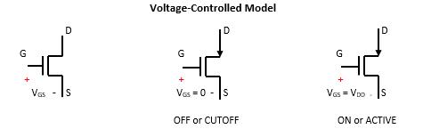
75
Fig. 4‐2. nFET voltage‐controlled model.
Logic‐Controlled Model D G = 0 (VGS = 0) G = 1 (VGS = VDD) S OPEN SWITCH CLOSED SWITCH (No electrical connection between D and S) (Electrical connection between D and S) Drain (D) Gate (G) I Control Source (S)
Fig. 4‐3. nFET logic‐controlled model.
Fig. 4‐1. nFET configuration.
2. pFETs utilize positively charged ion to facilitate current flow. pFETs also contain G, D, and S terminals. pFETs are the electrical and logical complements to nFETs. An example of a pFET is shown in Fig. 4-4 below.
I denotes the electric current, which flows from the source(S) to drain (D) terminal based on the value applied to the gate (G) terminal. G, again, is used to control whether the S to D connection for current I is on or off. Voltage and switch models are presented to show the electrical and logical relationships to turn the pFETs on/off to allow/cutoff electric current. In the voltage-controlled model (Fig. 4-5 below), the potential difference between S and G terminals (VSG) determines whether the transistor is on (allows electric current to flow) or off (cuts off electric current flow). When VSG = 0, the pFET is on, and the electric current I flows from the S and D terminals; VSG = VDD turn offs (cutoff) the current flow I from the S to D terminals.
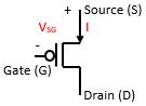
In order to translate the voltage-controlled model to allow or cutoff electric current cutoff, a corresponding logic-controlled model is presented as follows. In the logic-controlled model (Fig. 4-6), the VSD = 0 corresponds to a gate terminal logic value of G = 1 to turn off (cutoff) the D to S connection; the VSD = VDD corresponds to a gate logic value of G = 0 to turn on (allow) the D to S connection.
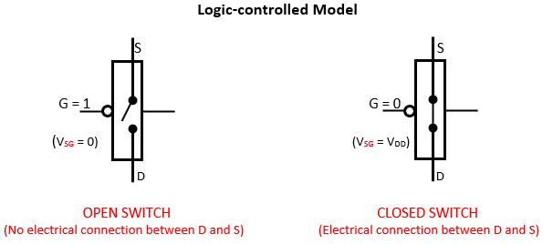
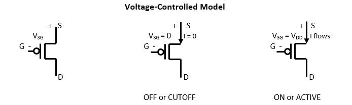
76
Fig. 4‐5. pFET voltage‐controlled model.
Fig. 4‐6. pFET logic‐controlled model.
Fig. 4‐4. pFET configuration.
Static CMOS logic circuits arrange nFETs and pFETs as complementary pairs, i.e. C in CMOS, sharing a common gate. In this arrangement, the value for the gate turns on one of the transistors, concurrently turning off the other transistor in the pair. If G = 0, the pFET is on, and the nFET is off. If G = 1, the pFET is off, and the nFET is on. Off and on do not refer to logical 0 and 1, respectively. Rather, off and on refer to whether the S and D terminals are electrically connected (on) or not (off). Fig. 4-7 shows complementary nFET and pFET pairs with a common gate (G) terminal.
G = 1 G = 0 (common G)
4.3 CMOS inverter
Consider the CMOS implementation of the inverter. There is a single input variable (X), which means there will be one nFET and pFET pair sharing a common gate terminal for X. The CMOS inverter implementation is given in Fig. 4-8 below.
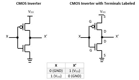
77
Fig. 4‐7. CMOS logic gates use nFETs and pFETs arranged in complementary pairs with a common gate (G).
OFF ON
ON OFF
Fig. 4‐8. CMOS inverter.
Notice in the CMOS inverter that the pFET has its source terminal connected to VDD and the nFET source is connected to reference (ground). The nFET and pFET pair share a common gate terminal and a common drain terminal connected to the output X’. The figure below shows the nFET and pFET on/off status for each value of X. When X = 0, the pFET is on, and the nFET is off. With the pFET on, the source and drain terminals are electrically connected. This means that the power supply VDD is connected to the drain terminal at the output X’. Concurrently, the nFET is off, meaning that the source and drain terminals are not electrically connected so that the ground is not connected to the output X’. When X = 1, the nFET is on, and the pFET is off. With the nFET on, the source and drain terminals are electrically connected with the ground connected to the output X’ (X’ = 0). At the same time, the pFET is off so that the power supply VDD is not electrically connected to the output X’. The convention used for the CMOS inverter having the pFET source terminal connected to the power supply VDD and the nFET source terminal connected to ground is commonly used in static CMOS to utilize the electrical property strengths of pFETs and nFETs. The passthrough voltage characteristics of nFETs and pFETs maintaining the integrity of low and power supply voltages, respectively1.
4.4 Transistor Connections
The CMOS inverter illustrates the nFET and pFET pair connections sharing a common gate. For static CMOS, there are two ways that MOSFETs are connected, series and parallel, as presented in Fig. 4-9 (series) and Fig. 4-10 (parallel) below.
78
4
Series Connection (End‐to‐End) X A ON For X to be electrically connected to Y, A = 1 (ON) AND B = 1 (ON) B ON LOGICAL AND: A∙B Y
Fig.
‐9. Series MOSFET connections.
Parallel Connection (End‐to‐End)
For X to be electrically connected to Y, A ON B A = 1 (ON) OR B = 1 (ON)
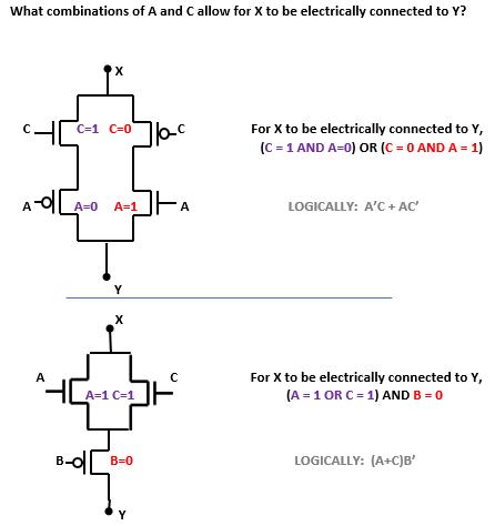
LOGICAL OR: A + B
variable combinations to create electrical connections between
79
Fig. 4‐10. Parallel MOSFET connections.
Fig. 4‐11. Series and parallel MOSFET combinations for
circuit points.
X
Y
Above are two examples (Fig. 4-11) of the series and parallel transistor connections to determine variable combinations to turn on transistor combinations to allow circuit points (x and y in the examples shown) to be electrically connected. These circuit point electrical connections are used in CMOS logic gates and combinatorial functions to provide paths to connect the power supply (VDD) (logical 1s) or reference (ground) (logical 0s) to the gate or function output.
As previously mentioned, nFETs are conventionally associated with the ground connection to electrically connect ground to the function output to provide the 0s in the function truth table. The pFETs are conventionally associated with the power supply VDD to electrically connect VDD to the function output to give the 1s in the function truth table. The array of nFETs and pFETs for two variable functions is shown in the Fig. 4-12 below.
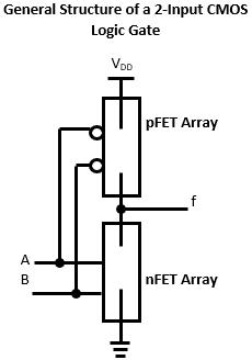
Consider the two input NAND gate and its truth table for determining the CMOS implementation. Using the pFET and nFET array connection conventions, the pFET array is based on the functional
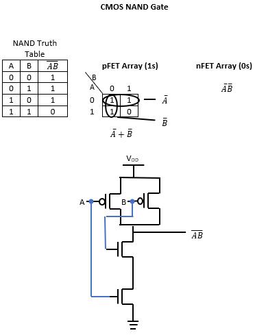
80
Fig. 4‐12. 2‐input CMOS logic gate structure.
Fig. 4‐13. CMOS NAND gate derivation and configuration.
form implemented based on the 1s entries from the truth table. From the K-map for the NAND truth table, the 1s entries yield the functional form A’+B’. Since a gate value of 0 turns on a pFET, a low value from a variable turns on a pFET. Accordingly, a complemented variable turns on a pFET. A’+B’ corresponds to connecting two pFETs in parallel with the source terminals of the pFETs connected to the power supply VDD. The nFET array is based on the function form based on the 0 entries from the truth table. From the K-map, there is only 0 entry for the grid slot AB. Since a gate value of 1 turns on an nFET, a high or uncomplemented variable value turns on an nFET. AB is implemented as two nFETs connected in series to ground. The drain terminals from the pFET and nFET arrays are connected together to provide the NAND gate output. The NAND gate input variables, A and B, are each connected to an nFET and pFET pair. The NAND gate CMOS implementation is shown in Fig. 4-13 above.
In the following example (Fig. 4-14), a CMOS logic function is presented for the two variable function Z(A,B). The transistors are labeled Q1, Q2, …, Q6. The truth table shows the input variable (A,B) combinations with each transistor ON/OFF status and output (Z) value (H for 1 and L for 0). For each input combination of A and B, the nFETs and pFETs for Q1 through Q6 are determined to be ON or OFF based on the gate value applied at each transistor. In determining the ON/OFF combinations and the resulting output Z, work left to right from the specified input values for A and B to toward the output Z. For the input combination AB = 00, the pFET Q2 has a 0 at the gate, which turns Q2 ON; the nFET Q1 has a 0 at the gate, turning Q1 OFF; the pFET Q4 has a 0 at the gate to turn Q4 ON; the nFET Q3 has a 0 at the gate, turning Q3 ON. The gate value shared with Q5 and Q6 is based on the electrical connection created from the Q1/Q2 combination for AB = 00. For AB = 00, Q1 and Q2 are found to be OFF and ON, respectively. Since Q2 is ON, the common connection point (common drain) between Q2 and Q1 is electrically connected to VDD, a logic 1 for this gate position to Q5 and Q6. Since there is a logic 1 for the gate to Q5 and Q6, the nFET Q5 is ON, and the pFET Q6 is OFF. Finally, the output Z is connected to the pFET parallel combination of Q4 and Q6 and the nFET series combination of Q3 and Q5. Thus, Q4 or Q6 must be ON to electrically connect VDD to the output Z to yield a high (H or 1), and Q3 AND Q5 must be ON to electrically connect ground to the output Z to give a low (L or 0). For AB = 00, Q4 is ON and Q6 is OFF. With Q4 and Q6 connected in parallel, Q4 provides a path for VDD to be electrically connected to the output Z, making Z a logic 1. Concurrently, note that Q3 and Q5 are in series, requiring both nFETs to be ON to provide an electrical connection between ground to the output Z for Z to be a logic 0. For AB = 00, Q3 is OFF and Q5 is ON, so that the ground is NOT electrically connected to ground. As a second AB combination, consider AB = 10. With B = 0, the pFET Q2 is ON and the nFET Q1 is OFF. With A = 1, nFET Q3 is ON and the pFET Q4 is OFF. The gate value for the nFET Q5 and pFET Q6 pair. This gate value is determined as the pFET Q2 is ON and the nFET Q1 is OFF, creating an electrical connection between the power supply VDD for a gate logic value of 1. Accordingly, the nFET Q5 is ON and the pFET Q6 is off. Since the series connection of nFETs Q3 and Q5 are ON, the ground is electrically connected to the output Z. Thus, Z = 0 for the input combination AB = 10. A similar process is applied to the other AB combinations to first determine the Q1 to Q6 transistor ON/OFF status, which produces the electrical path between ground and Z and between VDD and Z for logical 1s and 0s.
81
L L OFF ON OFF ON ON OFF H
L H ON OFF OFF ON OFF ON H
H
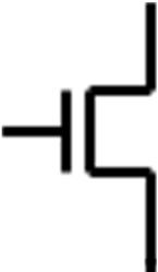

L OFF ON ON OFF ON OFF L H H ON OFF ON OFF OFF ON H
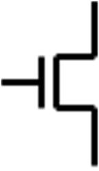
82
A B
Z
Fig. 4‐14. CMOS logic function with truth table derivation based on MOSFET ON/OFF combinations.
Q1 Q2 Q3 Q4 Q5 Q6
B A 0 1 0 1 1 A’ Z = A’ + B 1 0 1 B VDD A Z Q2 Q3 B Q1 Q4
Problems: (1) What is f? (2) Determine the nFET array.

Solution: (1) What is f?
pFET Array: �� �� ���� pFETs: Connected to VDD to give logical 1s in truth table A is connected in parallel to the series connection of B and C
Solution: (2) Determine the nFET array.
Array is based on connection to ground (0s)
83
table
on
A B C ���� �� F Derivation of f 0 0 0 1 1 1 �� ���� ���� 0 0 1 0 1 1 �� ���� ���� 0 1 0 0 1 1 �� ���� ���� 0 1 1 0 1 1 �� �� �� �� �� 1 0 0 1 0 1 �� ���� ���� ���� ���� 1 0 1 0 0 0 �� �� ���� ���� ���� 1 1 0 0 0 0 �� �� 1 �� �� ���� 1 1 1 0 0 0 �� �� ���� (Verifies f) BC A K‐map of f 00 01 11 10 nFET
0 1 1 1 1 AC �� ���� ���� �� �� ��
1 1 0 0 0 AB nFET
A(B+C)
VDD B A C f nFET Array
Truth
based
f
(derivation of f is above)
Array: B+C (parallel),
(series)
Fig. 4‐15. CMOS circuit example to find the logic function and nFET array.
In the CMOS circuit example above (Fig. 4-15), the pFET array is given with three input variables, ABC, and output f. With the pFET array given, the inputs ABC determine which pFETs are ON/OFF for creating or preventing an electrical connection path between the power supply VDD and the output f. Since pFETs are active low, i.e. require a logic 0 at the gate to turn them ON, the logical expression for f can be directly found from the pFET array. Specifically, pFETs B and C are connected in series, which is in parallel with the pFET A. Thus, f = B’ C’ + A’. In order to find the nFET array, two approaches can be used: 1) apply the logical dual and 2) find the function truth table and determine the expression for f’ from the functional 0s in the truth table. For approach 1, DeMorgan’s theorems are given as (AB)’ = A’+B’ and (A+B)’ = A’B’. Notice in (AB)’ = A’+B’, that the AND operation on the left-hand side is replaced with the OR operation on the right-hand side. Since (AB)’, the individual variables are complemented in replacing the AND with OR on the right-hand side (A’+B’). The logical dual for (A+B)’ is given by replacing the OR operation with the AND operation and complementing the individual variables (A’B’). pFETs are conventionally turned ON with 0s at the gate terminal and nFETs are conventionally turned ON with 1s at the gate terminal. Furthermore, the pFET array provides the electrical connection paths between the function output and the power supply VDD, and the nFET array provides the electrical connection paths between the function output and ground. Consequently, the pFET and nFET arrays provide logical dual connections in the other array. Applying logical duals, parallel connections of pFETs are replaced with series connections of nFETs, and series connections of pFETs are replaced with parallel connections of nFETs.
In the case of finding the nFET array for the function f from Fig. 4-15, the series (AND) combination of pFETs is replaced by an nFET parallel (OR) connection, and the pFET parallel
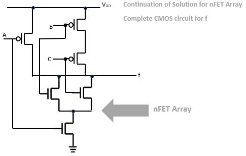
84
Fig. 4‐16. nFET array solution and complete CMOS circuit for problem (2) from Fig. 4‐15.
connection between A and the series connection of B and C is replaced by an nFET series connection between A and the parallel connection of B and C. The complete CMOS implementation including the derived nFET array is shown below in Fig. 4-16 above.
For approach 2, the function f is found from the pFET array directly as f =A’+B’C’. Note that only function 1s are specified in the pFET array. The remaining entries in the truth table are unspecified electrically, not necessarily 0s. In order to completely specify the truth table, the 0 entries must be configured in the nFET array. Using the function f=A’+B’C’, the 1s entries in the truth table can be determined. The remaining entries are specified as 0s in the truth table. Since the nFET array provides the connection between ground and the output f, the K-map is examined to find the minimal sum function (f’) from the 0s. From the minimal sum function (f’), uncomplemented variables in terms correspond to direct connections between the input variables to the gates of the nFETs. Complemented variables in terms from f’ require adding a CMOS inverter from the input variable and taking the complement of the variable as the gate terminal for the nFET. This process is shown in Fig. 4-15 with the nFET array presented in Fig. 4-16.
In the final example (Fig. 4-17), consider the implementation of the CMOS OR gate. The truth table for the OR gate is given below. Using the static CMOS convention with the pFET array connected to the power supply and the nFET array connected to ground. For the pFET array, the convention uses the 1s in the truth table (and K-map) to obtain a minimal SOP expression for the OR function A+B. Complemented variables in the minimal SOP expression correspond to direct connections from the input variables to pFETs in the pFET array. Uncomplemented input variables must be taken through a CMOS inverter with the output of the inverter connected to pFETs in the pFET array. From the truth table for the OR gate, the 1s entries yield a minimal sum of A+B, both uncomplemented variables. Similarly, for the nFET array, the convention uses the 0s in the truth table (and K-map) to obtain the minimal SOP expression for NOT OR ( (A+B)’ ) or A’B’. nFETs by convention have uncomplemented variables passed to the nFETs in the nFET array. In this case, both variables are complemented, which is the opposite of the standard conventions for static CMOS. Since the pFET and nFET arrays both have the opposite input variable forms to the standard convention, there are two approaches that can be used to implement the OR gate: 1) invert variables and then use the standard convention, or 2) implement the complement to the function and invert the function. For approach 1, the input variables A and B are input to CMOS inverters to give A’ and B’. A’ and B’ are passed as the gate values to a parallel pFET combination for the pFET array and corresponding series nFET combination for the nFET array. This yields (A’)’ + (B’)’ = A+B from the pFET array or (A’B’)’ = A’’+B’’=A+B from the nFET array. This configuration uses 8 MOSFETs (2 CMOS inverters with 1 pFET/nFET pair in each; 2 pFET/nFET pairs for the 2-variable function). For approach 2, the pFET and nFET arrays using the standard convention implement the opposite form of the function, namely (A+B)’. Therefore, implement (A+B)’ using the standard static CMOS convention and pass the output from this operation to the gate terminals for a CMOS inverter to yield (A+B)’’=A+B. In this implementation, the input variables are passed to the gate terminals of 2-variable pFET/nFET pairs to generate the output (A+B)’. To produce this output, the input variables are passed to the gate terminals of two nFETs connected in parallel with corresponding pFETs connected in series. (A+B)’ is passed as the gate terminals to a CMOS inverter to produce (A+B)’’ = A+B. This CMOS
85
implementation uses 2 pFET/nFET pairs to produce (A+B)’ and 1 pFET/nFET pair for the invert operation to require 6 MOSFETs to implement the static CMOS OR gate. The CMOS OR gate implementation using approach 2 is shown below.
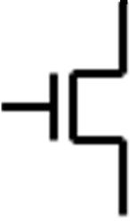
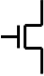
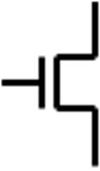
1 Uyemura JP, A First Course in Digital Systems Design: An Integrated Approach, Brooks/Cole Publishing, 1999.


86
OR Gate A B A+B 0 0 0 0 1 1 1 0 1 1 1 1
Fig. 4‐17. CMOS OR gate.
Reference
VDD A �� �� B A+B
CMOS OR Gate Implementation (NOR‐NOT)
Chapter 5: Digital Components
Chapter 5 Learning Goals
Construct more complex digital devices from basic, Boolean-level devices
Design and implement digital circuits using digital devices
Chapter 5 Learning Objectives
Understand the concept of a Black Box Device
Define how an Adder Device functions
Construct a multi-bit Adder and perform unsigned and 2's complement addition
Construct Adders to perform Integer multiplication, Selectable add/subtract function, and combinations of other Adder functions
Implement combinatorial functions on programmable logic arrays (PLA)
Implement simplified functions in a PLA, be able to switch from AND/OR to OR/AND PLA
Define how an Equality Comparator functions
Define how a Magnitude Comparator works
Understand how a Multiplexor (Mux) works and multi-bit Multiplexors are constructed
Combine Comparators and Multiplexors to implement complex functions
Implement combinatorial logic with a Mux
Implement more complex logic with Muxes and Gates
Define how a Decoder works
Implement combinatorial logic with a Decoder
Define how Encoders and De-Multiplexors work
Understand the concepts of active-high and active-low for digital component enable and outputs
Calculate delays and timing in a digital system
87
In this chapter, we will be constructing devices that will implement combinatorial functions and more complicated actions, such as comparison of numbers and routing of digital signals. We give these more advanced devices the title “Black Box” in the sense that the shape no longer represents the operation, e.g., the AND gate and OR gate shapes indicate their function. The label on the box will indicate the function.
5.1 Comparison of binary numbers
Many times, two multi-bit binary numbers will need to be compared to see if one number is greater than, less than, or equal to the other. The result of this comparison could then be used as a control signal or for some other purpose later on in the logic system. We will examine two types of comparison devices here, namely, the equality comparator and the magnitude comparator.
5.1.1 Equality Comparator
The purpose of the equality comparator is to indicate if two multi-bit binary numbers are equal or not. We want our device to output a logic 1 (true) if the two numbers are equal, and a logic 0 (false) if the numbers are not equal. Let’s begin by examining how we would determine if the numbers are equal or not and then translate that into digital components.
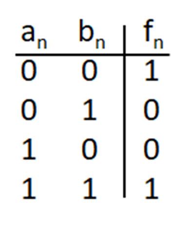
Let’s say that we have two 4-bit numbers A and B. Let the binary value of A = 1011 and B = 1001. We look at these numbers and we can instantly tell that they are not equal. We know this because the second bits from the right are different, therefore the numbers are not equal. However, how do we have a hardware device do this? In actuality, what we did is we looked at each bit in the sequence and made a determination if the numbers are equal or not. We can follow that same procedure if we can come up with a way to determine if two bits are equal or not.
We can start to figure out what we can use by looking at a simple truth table for a pair of bits. Let’s look at the table for the nth bits of our two numbers:
This truth table says that if an equals bn, the same then our output function for the nth bit should be a 1. If an and bn are different then the output should be a 0. In other words if the value is the same the two bits are equal if they differ then they are not equal. We can now write the function:
We see that the function is a simple XNOR gate to determine if two bits are equal or not. However, that is just for a single pair of bits, what about the other three bots in our 4-bit example? Assuming
88
�� �� �� �� �� �� ⨁��
that each pair of bits will be connected to an XNOR gate we can determine the equality of each pair using the diagram presented in Fig. 5-1.
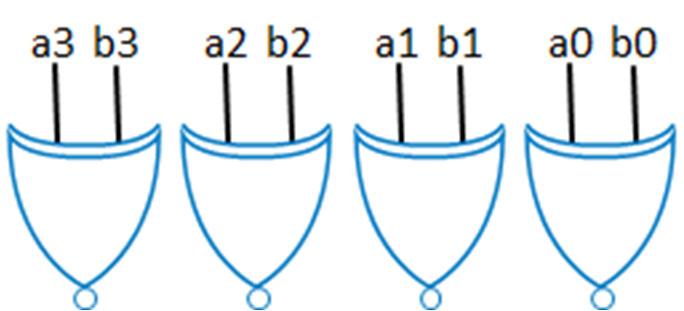
This circuit tells us if each pair is equal or not, but we want to know if the entire numbers, A and B, are equal. The solution to this is a simple AND gate. Since each pair is producing a 1 if the pair is equal, the only time the full 4-bit numbers are equal is if all four values are 1. We recognize this as the function of an AND gate, and we can now complete the diagram for the equality comparator, given in Fig. 5-2 below.
If we had to draw the above diagram every time, we wanted to use an equality comparator, this would become very tedious. Instead, we will replace the diagram using XNOR and gates with a single box, i.e. digital component, as shown in Fig. 5-3.
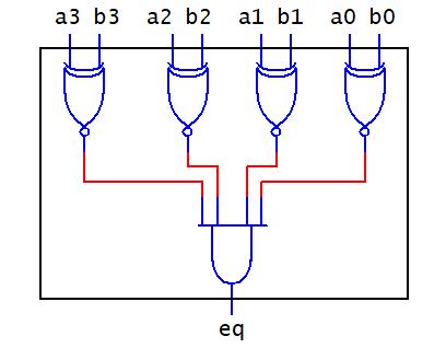
89
Fig. 5‐1. Individual bit comparisons for equality comparator.
Fig. 5‐2. Equality comparator logic network.
Notice, we have the two 4-bit numbers A and B in terms of their component parts coming into the box, and a single line (eq) coming out where eq is the output function:
���� 1; ���� �� �� and ���� 0; ���� �� ��
We can further simplify our black box using what is known as bus-notation, as shown in Fig. 54.
Here, we replace the four input lines for each variable A and B with a thick line with a slash through it. The number next to the slash indicates how many lines are contained in the thick line. We would say that the thick lines with the slash, and the number 4, are 4-bit bus-lines and represent the four bits that make up each binary number A and B. We have also removed the label “4-bit equality comparator” and just replaced it with a simple equal sign to represent that this is an equality comparator.
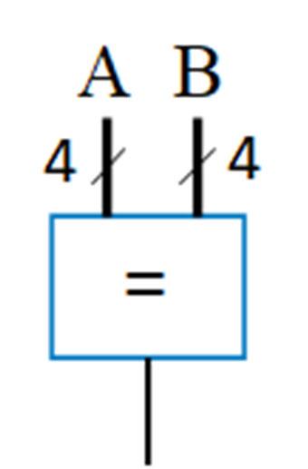
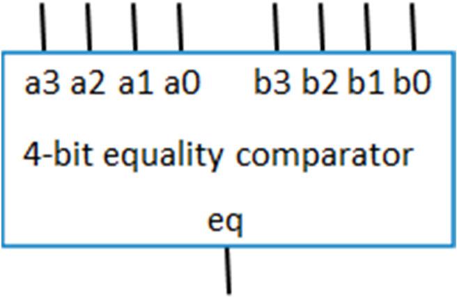
90
Fig. 5‐3. 4‐bit equality comparator digital component.
Fig. 5‐4. Equality comparator represented using bus‐notation.
5.1.2 Magnitude Comparator
What if we need to know more than just if two binary numbers are equal? We may want to know if one number is greater than, less than, or equal to another. We need a magnitude comparator. Once again, let’s examine how we would determine one number is greater than, less than, or equal to another.
Let A and B be two 4-bit, binary numbers. Again, let A = 1011 and B = 1001. We saw with the equality comparator that we examine each pair of bits for equality. This time we expand that to include greater than and less than in the examination; but we still do so pairwise. The one caveat for the magnitude comparator is that we must start from the left, the most significant bit position, and move right, towards the least significant bit position, in the comparison. When comparing A and B in this case, we see that the leftmost bits for both A and B are ones. We cannot make any determination, but we know we have to look at the next pair of bits. The next bits for our A and B are both zeros. The same situation exists where we can’t determine if the numbers are greater than, less than, or equal to each other. So, we move to the third bit from the left. This time, we see a1 = 1 and b1 = 0. At this point, we can determine that A is greater than B. Anything to the right of this bit is not relevant to determining if A is greater than or less than B. Only if all numbers are equal will the output indicate if A = B.
Now, let’s build our black box. This time we will show the box and then determine the functionality inside the box. For the leftmost stage, let the box be as shown in Fig. 5-5.
The box has an a and b input for the leftmost bits of A and B. It has the outputs out_gt when a>b, out_eq when a=b, and out_lt when a<b. This stage only works with the leftmost bits and will tell the next stage what the results of the comparison of this stage. Notice, only one of the outputs will be a 1 and the other two will be 0 at any given time. So, if out_gt is 1 we know that A>B and no other stage has to do any comparison, likewise if out_lt is 1 then A<B. The next stage only has to perform the comparison of the next two bits if out_eq is 1.
The next stage must include the results of the previous stage. We add three inputs: in_gt, in_eq, and in_lt. If in_gt is 1 then out_gt must be 1 and the other two should be 0. If in_lt is 1 then out_lt must be one and the other two 0. Only if in_eq is 1 do we do the comparison of these two bits. This stage has the diagram shown in Fig. 5-6.
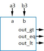
91
Fig. 5‐5. Black box most significant bit comparison.
In fact, each successive stage would have the same structure with only the final stage giving the final output to determine if A>B, A=B, or A<B. For the 4-bit example magnitude comparator example, the digital component diagram is given in Fig. 5-7.
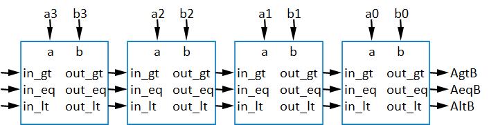
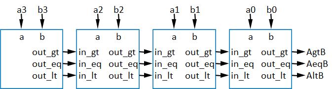
Note, only the first stage is different, meaning that we have a separate function for that stage. It would be much easier if we could use just one block and continue to repeat it. Furthermore, if all the stages are the same, we can add another set of four to either the front or back of the diagram to make an 8-bit comparator. So, we can simply replace the first stage with the same diagram we used for the other stages. The resulting diagram is shown in Fig. 5-8. We will have to come up with what we will enter into the in_gt, in_eq, and in_lt inputs:
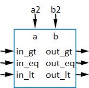
92
Fig. 5‐6. 1‐bit comparator component assuming in_gt, in_eq, and in_lt are determined from more significant bit position.
Fig. 5‐7. 4‐bit magnitude comparator diagram with comparison result given with outputs, AgtB, AeqB, and AltB.
Fig. 5‐8. 4‐bit magnitude comparator using cascaded 1‐bit comparator digital components.
Recall, if we want the second stage to perform the comparison of a2 and b2, we had to have the in-eq input be 1 and the other two had to be 0. We can use this information to simply set the inputs for the a3 and b3 stage, in_gt, in_eq, and in_lt, to the same 0,1,0, respectively.
Let’s open up the inside of the box. We see that if in_gt = 1, then out_gt must be 1. If in_gt is a 0, we next have to look at in_eq. If in_eq is a 0 that means that in_lt = 1 and out_gt = 0. However, if in_eq is a 1, and in_gt is a 0, we have to see if input a is greater than input b. If a is greater than b then a=1 and b=0 since a and b are bit values. If we want to output a 1 if a is greater than b and 0 otherwise, this is simply the equation a b. We now have all the information we need to write the equation for out_gt as:
We can use the same logic to determine the function for out_lt. If in_gt = 1, then out_gt = one. If both in_lt and in_eq are 0 then in_gt must have been a 1 so out_lt must be a 0. If in_gt = 0 and in_eq = 1 then we need to see if a<b. If a=0 and b=1 then a<b which we can represent by the function ab. The function for out_lt can be written as:
The function for out-eq is even simpler. We have to check if in_eq = 1. If in_eq = 0, then, either in_gt or in_lt was a 1 and will dominate the function. Only if in_eq = 1 will we need to see if a and b are equal. If in_eq = 1, then we use the same function as the equality comparator. The function for out_eq is:
The above equations are easily implemented for each stage of the magnitude comparator. The full diagram with all four stages is called a ripple-carry device. The information must ripple through each stage and only when the information is carried to the final stage is the output meaningful. The cost of this type of structure is that it takes time for the information to move through all the stages and we must wait for the device to finish before using the output.
5.2 Decoders
The next black-box device we will examine is a very useful device and is used in follow-on courses in Computer Engineering. A decoder is also called a line decoder in that a set of inputs activates a particular output line based on the input value. Decoders come in a couple of varieties, namely, active-high and active-low. Additionally, there is an enable line that can be used to turn the device on or off.
5.2.1 Active‐High Decoder
The active-high (AH) decoder uses positive logic to determine its output. It has a set of input lines and a set of output lines where the number of outputs is 2number of inputs. When referring to a decoder
93
������ ���� ���� ���� ���� ����∙ a ∙ b
������ ���� ���� ���� ���� ����∙ a ∙ b
������ ���� ���� ���� ���� ����∙ a⨁b
we specify the number of inputs x number of outputs and then if it is active high or low. A 2x4 AH decoder diagram is shown in Fig. 5-8 below.
The control word inputs are i1 and i0 and the outputs are y0 through y3. The enable line (en) is also shown. The truth table of the 2-to-4 decoder is shown in Fig. 5-9 below.
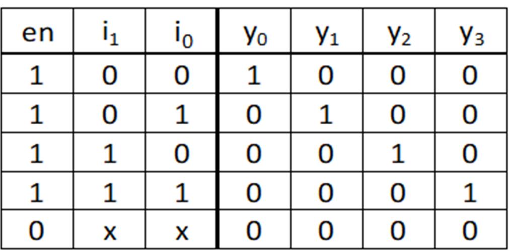
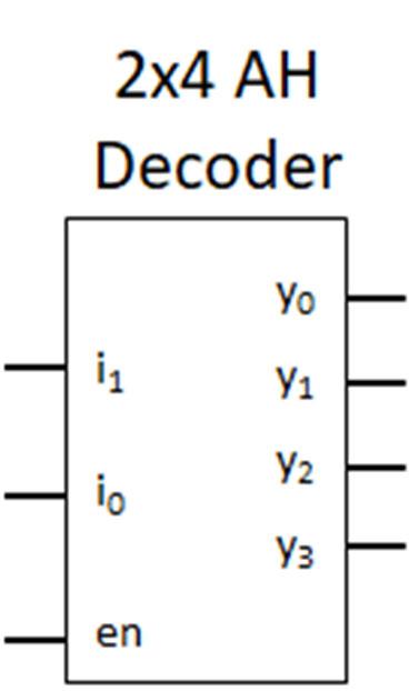
From Fig. 5-9, if the enable line (en) is 0, it does not matter what i1 and i0 are, all the output lines are 0. If en=1, however, then the line corresponding to the binary number made by i1 and i0 will output a 1 while the others are 0. This device can be used as a selector, or, as we will see, can be used to create SOP combinatorial functions.
The en line is connected to all four AND gates, so, if en=0 then all four AND gates will output a 0 as desired in the truth table. If en=1 we see that only one AND gate will output 1 for any given input on the i1 and i0 lines while the others will output a 0. For example, in en=1, i1=1, and i0=0 then only y2 will output a 1. The i1 and i0 lines in this configuration is a selector diagram, we will see this structure in other devices.
Let’s take a look at the inside of the black box for the 2x4 AH decoder in Fig. 5-10.
94
Fig. 5‐8. 2x4 AH decoder.
Fig. 5‐9. Truth table for 2x4 AH decoder.
4.2.2 Active‐Low Decoder
The active-low (AL) decoder uses negative logic to determine its output. Otherwise, it is very similar to the AH decoder. A 2x4 AL decoder is shown in Fig. 5-11.
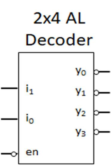
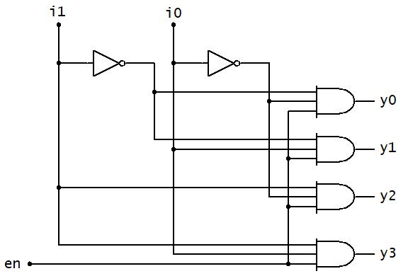
We see that for the black-box, the only difference between the AH and AL decoders is that the AL decoder has inverting bubbles on the outputs and the enable. The truth table for the AL decoder is given in Fig. 5-12.
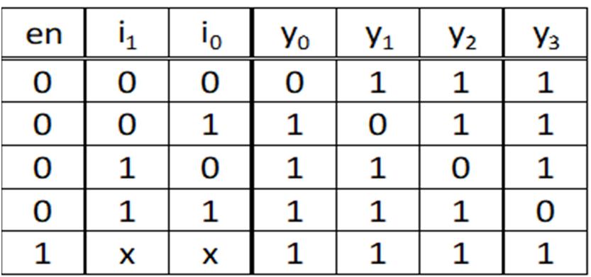
95
Fig. 5‐10. Logic circuit for 2x4 AH decoder.
Fig. 5‐11. 2x4 AL decoder diagram.
Fig. 5‐12. Truth table for 2x4 AL decoder.
For the AL decoder, if en=1 then all the outputs are set to 1. If en=0, then the output corresponding to the binary input i1 and i0 will be set to 0 while the others are 1. Once again, we see that this will act as a selector, albeit using a 0 to make the selection for the negative logic, but, more importantly, we will be able to make POS combinatorial functions. The inside of the box is also similar to the AH decoder, as given in Fig. 5-13.
One difference between the AH and AL decoders is that instead of AND gates, we use NAND gates for the AL decoder. The other difference is that the enable goes through an inverter. If en=1, then a 0 is applied to each NAND gate. A 0 applied to a NAND gate will force the output to 1, which is what we want from the truth table. If en=0, then a 1 is applied to the NAND gates and the input i1 and i0 will determine which output will be 0 while the others are 1. It is possible to mix and match active-high and active-low parts of decoders. For example, a decoder with active-high outputs and active low enable or active-low outputs and active-high enable are possible combinations. An active-high output outputs a 1 when selected and 0 otherwise, while active-low outputs output a 0 when selected and a 1 otherwise. An active-high enable activates the device when en=1, while an active-low enable requires en=0 to activate the device.
5.2.3 Combinatorial Functions Using Decoders
We will now show how to use decoders to create combinatorial functions. Let’s look at a 3x8 AH decoder (set en=1) with input variables A, B, and C. If we write a function for when each output will output a 1, we find when associated with the 3x8 AH decoder diagram as shown in Fig. 5-14.
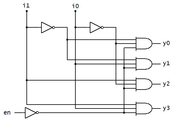
96
Fig. 5‐13. 2x4 AL decoder logic circuit.
From Fig. 5-14, we recognize these functions as the functions for minterms:
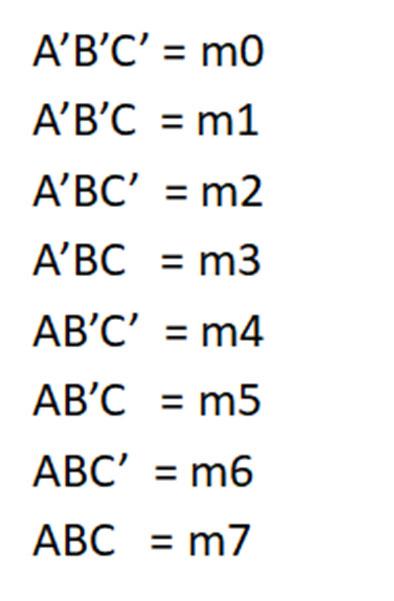
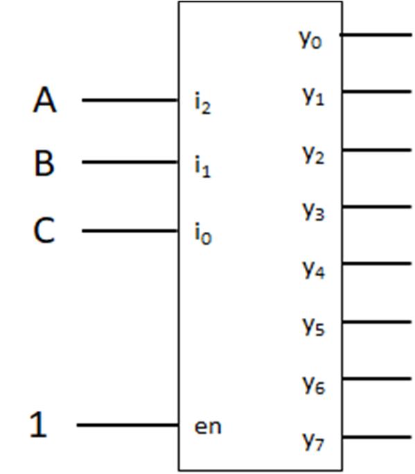
Recall that we can write any SOP combinatorial function as the sum of the minterms, e.g., �� ���� 1,2,5,7 . However, the sum is just an OR gate, so by simply ORing the outputs y1, y2, y5, and y7, the function F is generated (see Fig. 5-15).
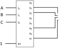
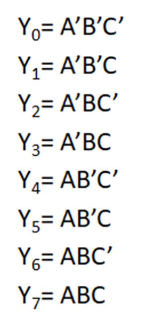
97
Fig. 5‐14. 3x8 AH decoder diagram.
F
Fig. 5‐15. Minterm expression for function F implemented using a 3x8 AH decoder and an OR gate.
A similar result can be achieved using AL decoders. This time, however, recall that AL decoders produce negative logic, but this is exactly what we see when using POS functions. Recall that POS functions and Maxterm functions are synonymous, so we produce a very similar diagram using an AL decoder as we did for the AH decoder, which is shown in Fig. 5-16.

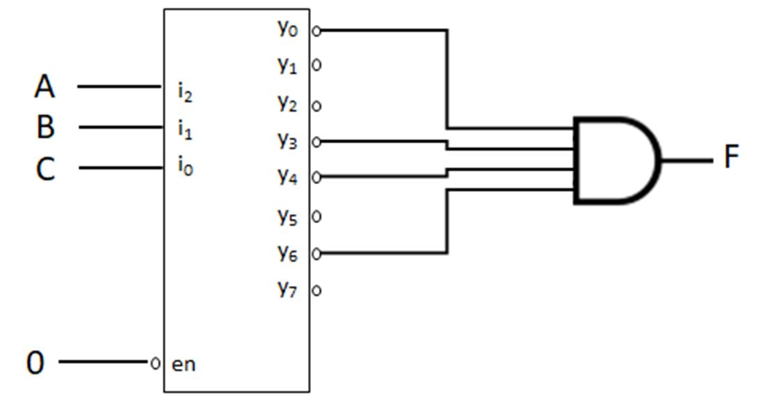
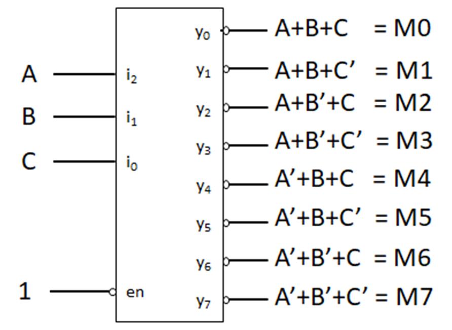
Since we can make combinatorial functions by AND’ing Maxterms, we only need to route the associated y term to an AND gate to generate a function. Using the previous example function, �� ���� 1,2,5,7 , we first convert this to the POS-based maxterm expression, �� ���� 0,3,4,6 . The resulting diagram for F is given in Fig. 5-17.
So, we see we can use OR gates with AL decoders and gates with AL decoders. It turns out we can use NOR gates with AH decoders and NAND gates with AL decoders. Let’s look at the mathematics:
98
Fig. 5‐16. 3x8 AL decoder diagram.
Fig. 5‐17. Maxterm expression for F implemented using a 3x8 AL decoder and an AND gate.
�� ��, �� , �� ���� 1,2,5,7 �� �� �� �� 0
This equation says that I can implement the function, F, using a NAND of the Maxterms. However, the AL decoder produces Maxterms, so we can use a NAND with the AL decoder to implement the function. A similar result can be produced starting with the maxterm expression:
Here, we can implement the function using a NOR gate of the minterms. However, an AH decoder will produce minterms that we can connect to a NOR gate. The diagrams in Fig. 5-18 show the implementation using NAND (a) and NOR (b) gates.
5.2.4 Expanding Decoder Capability
If we were to go purchase a decoder integrated circuit (IC) chip, the largest decoder we could readily find is a 3x8 Decoder. This means that we could only have three variables in our functions. This would not be very useful, but there are ways to expand the capability of the decoder by combining multiple decoders. We will be using the enable input to control when a decoder is on or off and not just locked on, like we have seen.
To see how we can extend the number of variable, let’s begin by taking a closer look at a 4variable truth table and associated minterms in Fig. 5-19.
99 �� �� �� �� �� ∙�� ∙�� ∙��
�� ��, �� , �� ���� 0,3,4,6 �� ∙�� ∙�� ∙�� �� ∙�� ∙�� ∙�� �� �� �� ��
(a) (b)
Fig. 5‐18. Decoder with NAND and NOR gate implementations of F. (a) Minterm expression. (b) Maxterm expression.
As noted on the figure, the 3-variable pattern inside each dotted line box is identical. The only thing differentiating between minterms 0 through 7 and minterms 8 through 15 is the value of the MSB, A. So, we can have minterms 0 through 7 as the output of one decoder and minterms 8 through 15 as the output of a second decoder. We use the variable A to control which of the two decoders is active. Recall that only one output will be 1 for an AH decoder, and if the enable is 0 all the outputs are 0. Therefore, by deactivating one decoder and then using variables B, C, and D to activate an output on the activated decoder, we produce the result we are looking for.
Fig. 5-20 (below) shows the diagram for a 4-variable decoder using two 3x8 AH decoders. Notice that the variables B, C, and D are connected to both decoders. The order of the variables and how they are connected is important! Let A be the most significant variable and D the least with order from most to least: A, B, C, D. The least significant input to the decoder is i0 and the most significant is i2. The variable D must be connected to i0, C must be connected to i1, and B must be connected to i2. If we look back at the truth table, we see that this diagram mirrors what we said about the patterns inside the dotted boxes. Now we need to determine how to use A to control which decoder is active. The decoders will activate if their enable inputs are 1, but we want the top decoder to turn when A=0 and the bottom decoder to turn on when A=1. So, if A=0, we need to insert an inverter before the enable of the top decoder. We see that the bottom decoder will be deactivated when A=0, but activated when A=1, and the top decoder will be the opposite, which is what we want. The output side is now just the minterms 0 through 15. Just as we did for a single decoder, we simply route the corresponding minterm output to an OR gate and we implement the 4-variable function.
100
Fig. 5‐19. 4‐variable truth table with minterms labeled.
For functions of more than four variables, we will use the same procedure to a larger extent. The 3x8 decoders will output the minterms, but for each variable over three we have to increase the number of 3x8 decoders by a power of two. For example, we just saw that 4-variables required two decoders, 5-variables would require four decoders, and 6 variables would need eight decoders. The variables above the least three significant variables will be used to control which decoder is activated. Let’s examine the diagram for a 5-variable function illustrated in Fig. 5-21 (below).
From Fig. 5-21, x0, x1, and x2 are the least three significant variables, x3 and x4 are used to control which decoder is activated. We see that x3 and x4 are used in the same selector diagram that we saw for a 2x4 AH decoder. In fact, we can replace the selector diagram with a 2x4 AH decoder with x3 connected to the i0 input, x4 connected to the i1 input, and the enable input connected to the voltage source or a constant 1. Using this technique, we can construct a function of any number of variables.
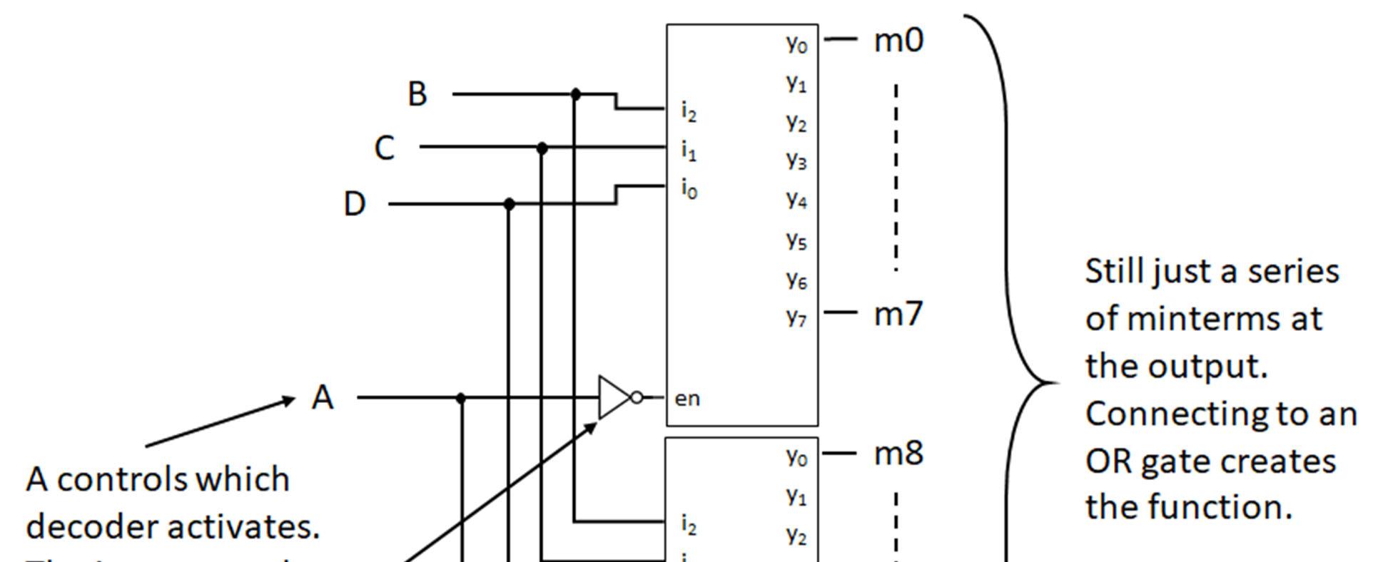
101
Fig. 5‐20. 3x8 AH decoder‐based layout for a 4‐variable function implementation.
5.2.5 Multiple Functions Using One Decoder
We conclude our decoder discussion by showing how to implement multiple functions using a single decoder. Let’s implement the functions �� ��, ��, �� ���� 2,5,7 and
���� 0,3,4 using a single 3x8 AL decoder. Note, that we can implement G directly with an AL decoder and an AND gate and can implement F using an AL decoder and a NAND gate. The diagram for these is given in Fig. 5-22.
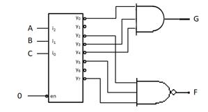
The implication of this capability is that we can make any number of functions that use the same input variables without the need of a decoder for each function. Furthermore, we can combine
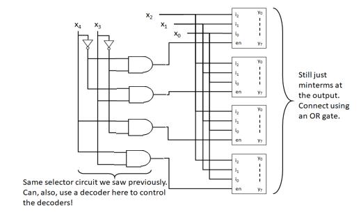
102
Fig. 5‐21. 5‐variable function implementation layout using 2x4 decoders.
�� ��, ��
��
,
Fig. 5‐22. Multiple function implementation using an 3x8 AL decoder with AND NAND gates.
decoder diagrams of more than 4-variables with the ability to generate multiple functions to produce a set of complex functions that we can use in our designs.
5.3 Multiplexor Devices
A multiplexor is best thought of as a selection device whereby we select one of several inputs to be routed to the output of the multiplexor (mux for short). The simplest example is that of a two input and one output mux. We will call this a 2:1 mux, as illustrated in Fig. 5-23.
The input lines are labeled D0 and D1 with the output labeled y. The s0 input is the selector line. If s0 is a 0, then whatever is connected to the D0 input will be routed to the output, y. If s0 is a 1, then whatever is connected to the D1 input will be routed to the output, y. This allows us to switch between two data sources to send out to whatever is next in design. Let’s take a look at how we construct a mux using logic gates, as shown in Fig. 5-24.
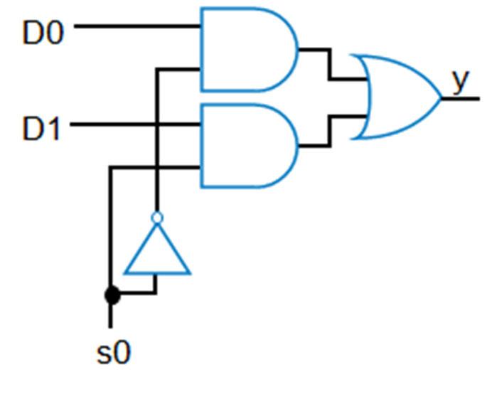
From 5-24, if s0 is a 0, then the lower AND gate will have a 0-input forcing the output of the AND gate to be a 0; however, the upper AND gate has a 1 input from the inverter which then passes whatever D0 has to its output. The OR gate has a 0 and D0 applied to it which means that D0 will be passed to the output y. If s0 is a 1, then the opposite happens. The upper AND outputs a 0 while the lower AND will output D1. D1 is then passed to the output y. We can now expand upon this concept to make larger mux devices. Let’s see what a 4:1 mux would look like (Fig. 5-25):
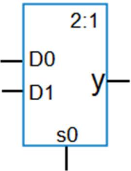
103
Fig. 5‐23. 2:1 mux diagram.
Fig. 5‐24. Logic gate implementation of a 2:1 mux.
Here we see that we have two selector inputs and four data inputs. The selectors, s0 and s1, have the same configuration as in the 2:1 mux with the non-inverted and inverted lines fed to the AND gates. However, we see that both selectors help determine which AND gate will pass its data line to the OR gate. In order to pass D0 we see s0 needs to be 0 and s1 needs to be 0 so that both inverters output 1 connected to the top AND gate. If we want D1 to pass through to the output, then s0 needs to be 1 and s1 needs to be 0. We can map this to a truth table like this:
Notice that the binary number made by s0 and s1 correspond to the decimal number of each data line. We also see that there is a direct relationship between the number of selector lines and the number of input data lines, namely, no. data lines = 2no. of select lines. So, an 8:1 mux would need three select lines in order to route one of the eight data inputs to the output.
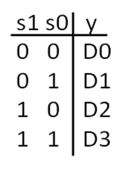
We will see there will be times when we want to route multi-bit variables and not just single bits. Suppose we want to select between two 4-bit variables A={a3, a2, a1, a0} and B={b3, b2, b1, b0} using the diagram in Fig. 5-26 (below).
Notice, each pair of the nth bit of A and B are connected to a 2:1 mux. However, all the select lines are tied together. So, if s0 is 0 then the A variable is selected and if s0 is 1 then the B variable is selected. We can simplify the black-box by using bus-notation in Fig. 5-27 (below).
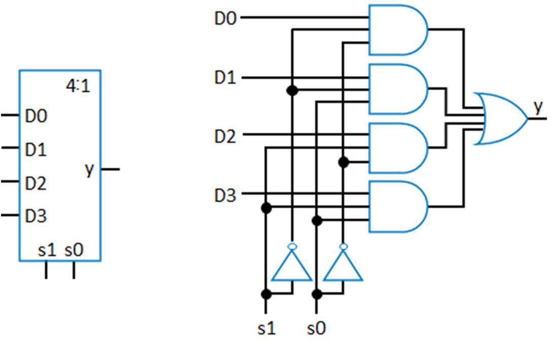
104
Fig. 5‐25. 4:1 mux diagram and logic gate implementation.
It is implied that all the lines of either A or B will be selected depending on the value of s0.
5.4 Complex Functions Using Digital Components
Using multiplexors and comparators it is possible to produce some complex operations such as finding the minimum and maximum of two binary numbers and performing IF/Then statements at the hardware level. Let’s start by designing a black-box that will find the minimum of two 8-bit binary numbers.
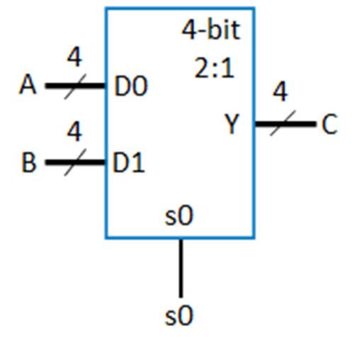
First, we will need to identify a device that can determine if a binary number is greater than, less than, or equal to another binary number. We have that in a magnitude comparator. Next, we will need to select the binary number that is the least based upon what the comparator tells us. Furthermore, the binary numbers are 8-bit. Again, we have this ability in the multi-bit multiplexor. In fact, with just these two devices we can complete the diagram of the minimum function as shown in Fig. 5-28 (below).
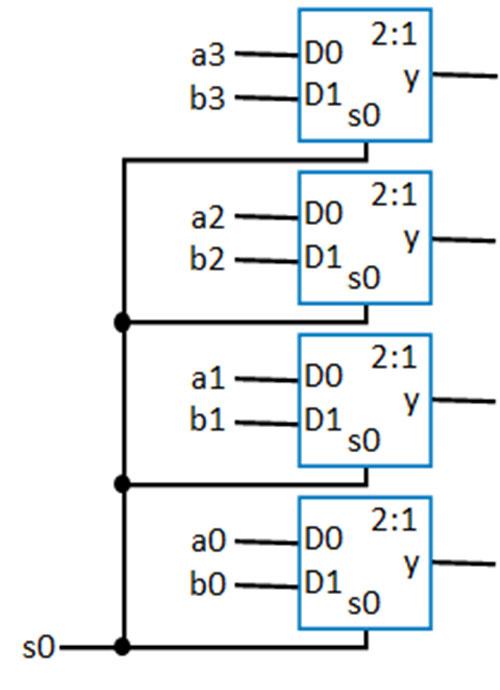
105
Fig. 5‐26. 4‐bit variable selector using 2:1 muxes.
Fig. 5‐27. Bus notation implementation of 4‐bit variable selector using 2:1 muxes.
From Fig. 5-28, we see that if the binary number A is greater than the binary number B, we want to select D0 so the smaller number is passed to the output. D0 is selected when s=0. The A<B output of the comparator will be a 0 if A > B. If A is less than B then the A<B output will be a 1 and s will select D1. Since A is the smaller of the two numbers, we have selected the correct value. If A = B, then it doesn’t matter which number we select since they are the same. In this case if A = B then the A<B output will be a 0 and the number B will pass to the output. Fig. 5-28 also shows the diagram to implement the function C=Min(A,B). To implement the function C=Max(A,B), we just have to switch the select line (Fig. 5-29)
From Fig. 5-29, we see if A is greater than B then the A>B output of the comparator will be 1 and the mux will select D1. Since A is greater than B, we have selected the correct output for the Max function. Likewise, A is less than or equal to B, then the A>B output will be 0 and the D0 line is selected as desired. We can now use our Min, Max, and other devices to implement more complex operations.
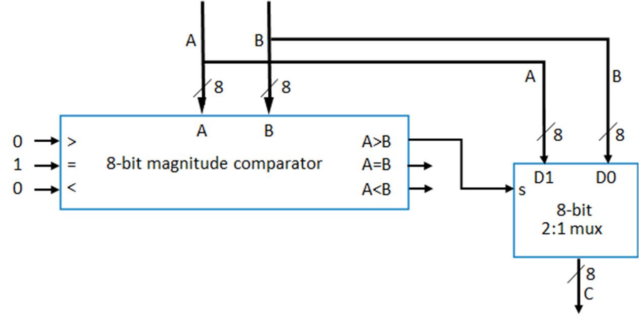
Let’s implement the operation: IF A=B THEN X=Max(C,D) Else X=Min(C,D), where A, B, C, and D are 8-bit binary numbers. For this operation, we need:
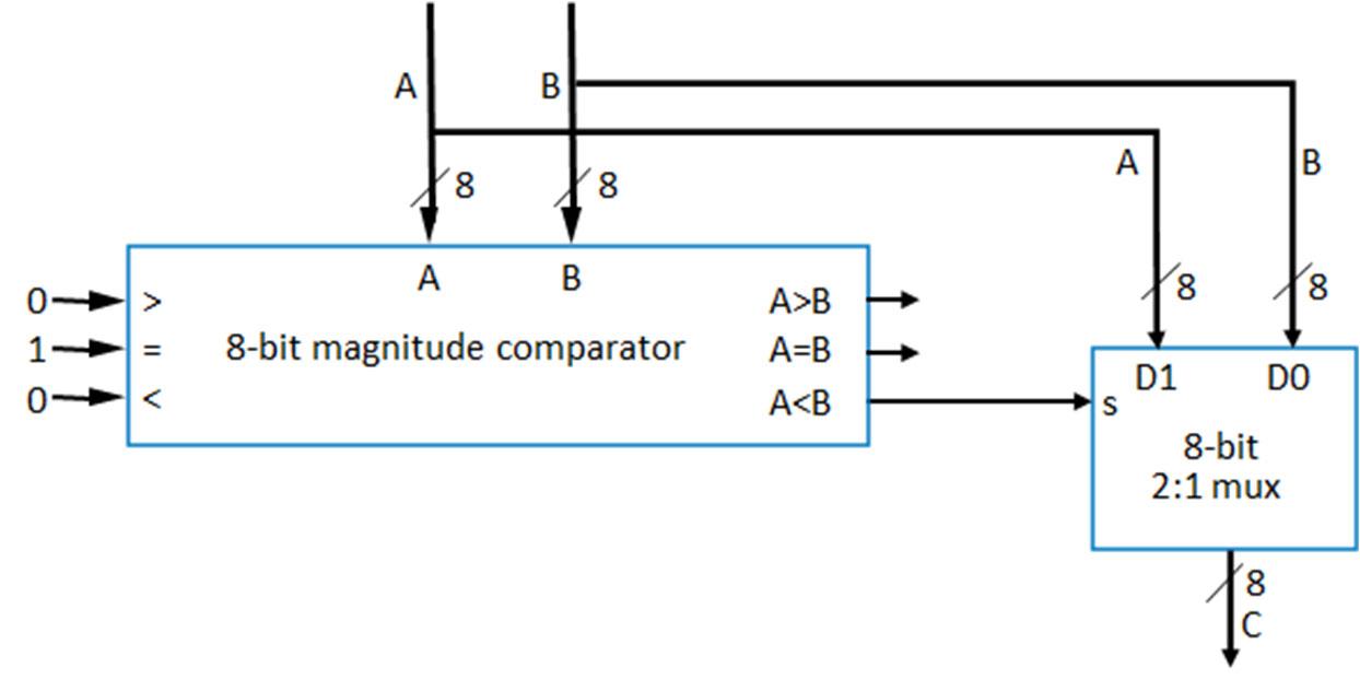
106
Fig. 5‐28. 8‐bit minimum number selector using a magnitude comparator and 2:1 muxes.
.
Fig. 5‐29. 8‐bit maximum number selector using a magnitude comparator and 2:1 muxes.
1. A way to identify if A equals B
2. Compute Max(C,D) and Min(C,D)
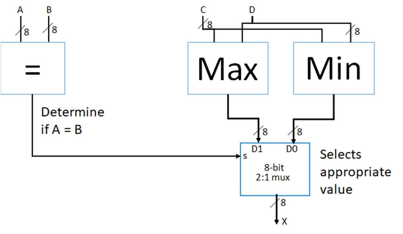
3. Select between the Max and Min functions
Obviously, we have all three of these needs. Our diagram for the IF/THEN operation is given in Fig. 5-30 below.
We can implement complex functions in hardware. In most cases, a hardware solution will operate more quickly than a computer program but is far less adaptable to multiple situations. If your application is doing the same process over and over again, it may make sense to implement a hardware solution, but if your application changes often, even small changes that would require a change in the circuit, a software solution may be what you need. Part of Computer Engineering is determining the best method.
5.5 Combinatorial Functions with Multiplexors
We can implement combinatorial functions using multiplexors. To see how this works, let’s examine a circuit where we have four binary variables A, B, C, D. Consider 4-variable function implemented using an 8:1 mux in Fig. 5-31 (below).
We see that A,B,C are used as the selector inputs. So, if all three are 0, the mux will select the input D0. However, the input D0 is the inverted variable D. If D is 0, F will be 1 and if D is 1, F will be 0. We can enter these values into a K-Map as follows:
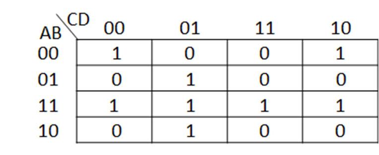
107
Fig. 5‐30. IF/THEN Max/Min selector using digital components.
Notice the first two boxes in the top row represent when A,B,C = {0,0,0}. The top left box is when D=0 and the next one to the right is when D=1. The output, F, like we calculated above is 1 when D=0 and 0 when D=1. If we move to the right two boxes on the top row, these correspond to when A,B,C = {0,0,1}. The D1 input would then be selected. Again, notice that D1 is connected to �� , so the value of F will again be opposite the value of D. As we move down each row, the pair of boxes represent values for A,B,C and will thereby select an input to the mux. Notice D2 is connected directly to D so the values for F follow D, but the input to D3 is a 0, so both entries for A,B,C = {0,1,1} are 0 regardless of the value of D.
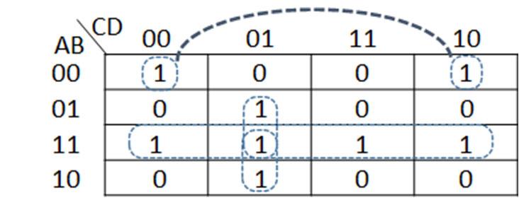
Once we have filled in the K-Map, we can then do the regular circling to reduce the function:
The function we implemented with this configuration is: �� ������ ������ ������ ����
Let’s now turn this around and start with a truth table and implement the function using a mux:
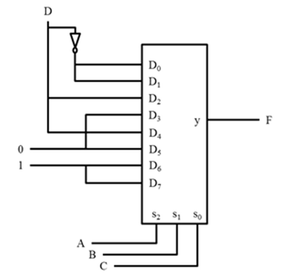
108
Fig. 5‐31. Example of a 4‐variable function implemented using an 8:1 mux.
We see this is a 4-variable function and using the procedures we learned for K-maps, we find the function is:�� ���� ������ ������ �������� �������� . If we were to implement this using 2input AND and OR gates and inverters, It would take 11 AND gates, 4 OR gates, and 4 NOT gates. Let’s take this same truth table, however, we will subdivide it into pairs of rows:
Furthermore, the D variable has been sectioned from A,B,C. For each pair, we see that the A,B,C values match for each row of the pair. If we compare the value of F with the value of D for each pair, we can write the sub-function of F for each of the pairs as shown. For example, when A,B,C = {0,0,0} the sub-function of F, �� �� . The sub-function is what we connect to input of our mux, shown in Fig. 5-32.
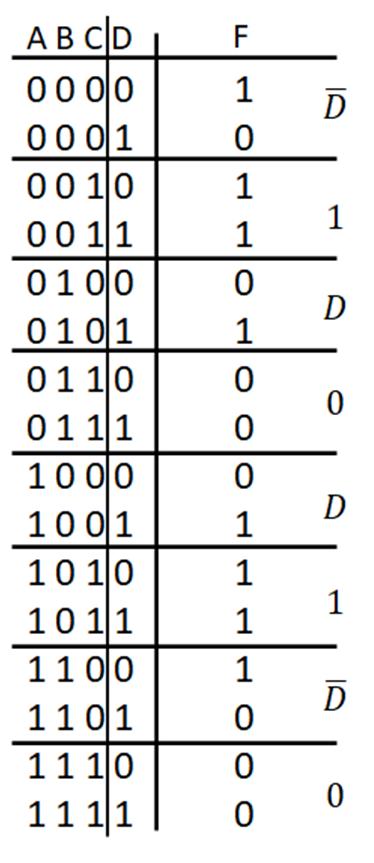
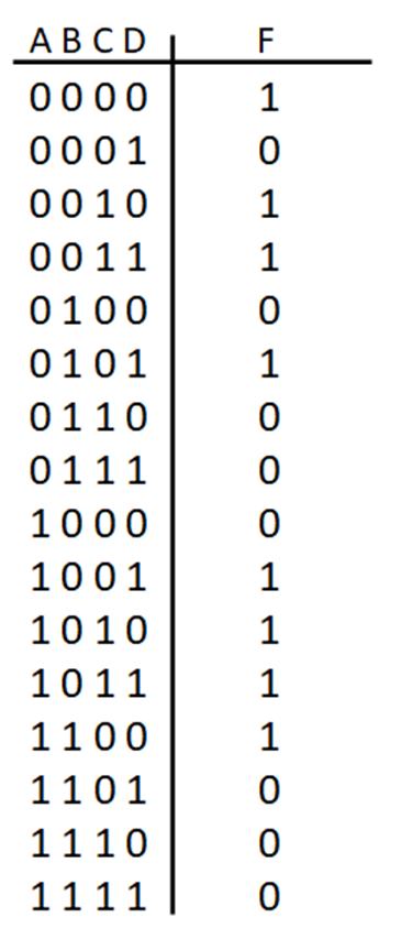
109
So, what was once going to be a complicated logic diagram with 19 gates is now very simple with a mux and a single inverter.
Suppose that we go to our parts bin only to find that we are all out of 8:1 multiplexors. However, we do have a 4:1 mux we can use, and several assorted gates. We can use a very similar technique to implement the function with the 4:1 mux and these gates. This time, instead of sectioning of just D, we will section of C and D and break our table into groups of four:
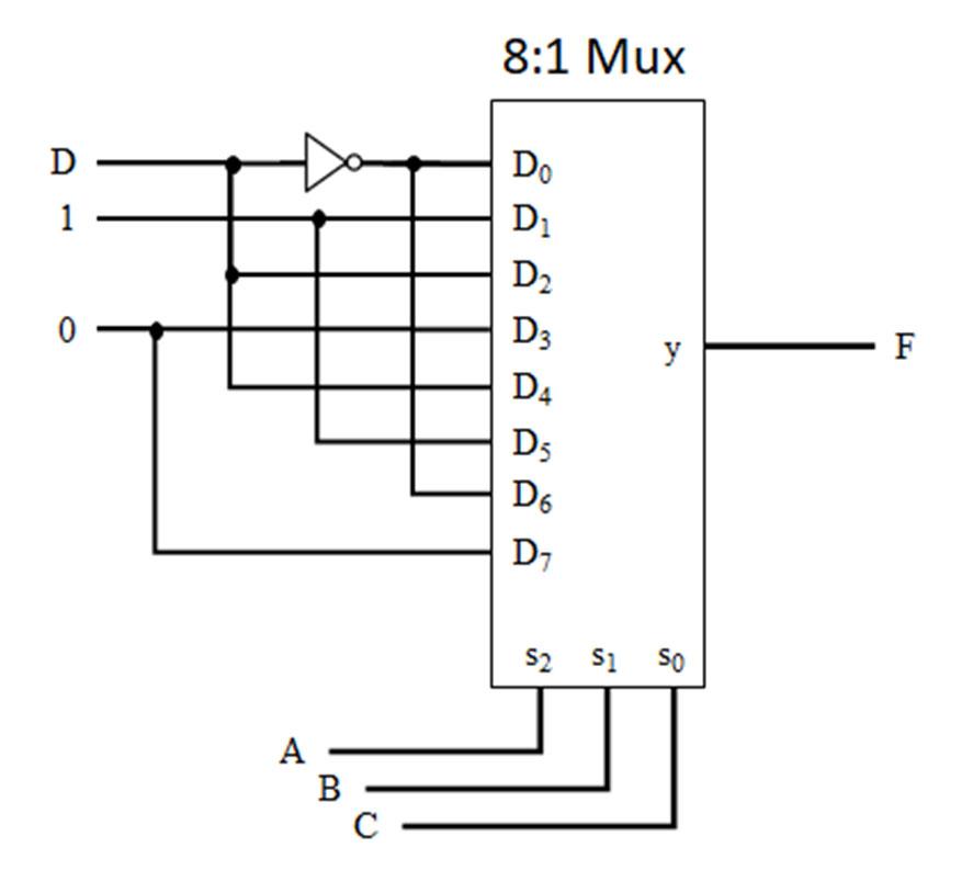
Here, we will make our sub-functions in terms of C and D for the four rows we have sectioned. Notice a and B again match for the sectioned rows and will be used as the selector inputs to the mux. Looking at each group of four rows, we can identify a sub-function of F in terms of C and D as shown in the table. Again, these four sub-functions are used as the input to our 4:1 mux, as shown in Fig. 5-33 (below).
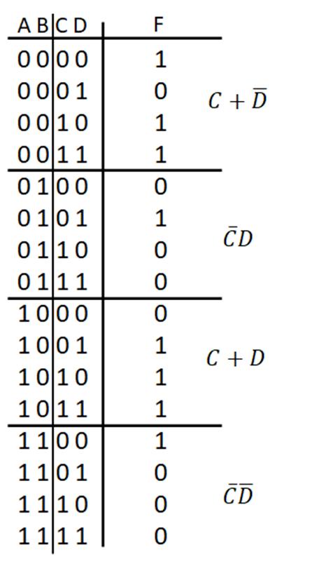
110
Fig. 5‐32. Example sub‐function implementation connected to an 8:1 mux.
This diagram only took two 2-input AND gates, two 2-input OR gates, two inverters, and the 4:1 mux. While a little more complicated than the 8:1 mux implementation, it is still far simpler than the discrete gate implementation. We can now implement any 4-variable, or fewer, function with a standard mux.
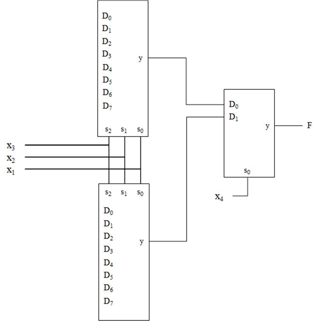
If we need to implement more than four variables, there is not a standard size of mux to accommodate the increased number of inputs (8:1 is typically the largest readily available mux in a standard IC). We could calculate the sub-functions as we did for the 4:1 mux, but this would get a bit cumbersome, particularly as we move up to 6-variables. We can, however, cascade the multiplexors. An example of the cascaded multiplexers is given in Fig. 5-34.
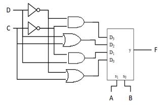
111
Fig. 5‐33. Example sub‐function implementation connected to a 4:1 mux for the same function from Fig. 5‐32.
Fig. 5‐34. Cascaded multiplexer example to implement a 4‐variable function.
We see here that x1, x2, x3 are selecting a particular input on the 8:1 muxes. The variable x0 would then be connected to the inputs as either non-inverted, inverted, or as just a 0 or 1, as we saw previously. x4 then selects which mux to use. For example, let x4,x3,x2,x1,x0={10110}. This sequence would select D3 from each 8:1 mux, but only the D3 from the lower mux would be selected to go to the output. Let’s say that x0 is inverted before connecting to the lower D3. Since x0 is 0 in our example, the output F will be 1. We can build the output function just as we did in the case of 4-variable, i.e., subdivide the truth table into pairs of rows and calculate each subfunction in terms of x0. Obviously, it doesn’t take much before using a mux or a decoder becomes somewhat unwieldy for large numbers of variables. There is another device we will examine later in this chapter that is made for such functions.
5.6 De‐multiplexors and Encoders
While multiplexors and Decoders are quite common in the digital logic world, each has a less-used cousin that are specialized in what they do. While the applications are less numerous, if you need their capability in your design, it is hard to find a replacement.
5.6.1 Encoder
Where a decoder took a binary number as its input and activated a single output line, an encoder does just the opposite. An encoder indicates, via a binary number, which line is activated. If an encoder has 2n inputs, there are n-outputs. An encoder example is shown in Fig. 5-35.
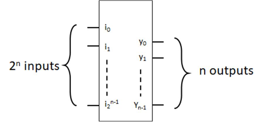
If line i0 is activated (i.e., it has the value of 1, it is assumed all other lines are 0) then the outputs will all be 0. We can put this into a pseudo-truth table (in this case for an 8x3 encoder), as observed in Fig. 5-36.
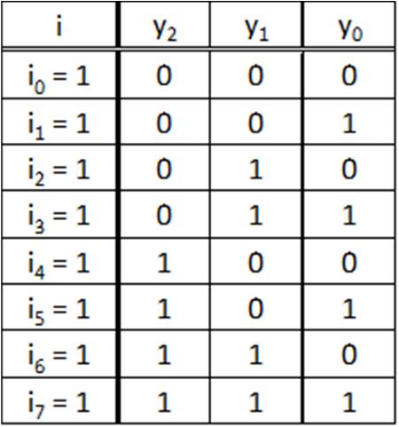
112
Fig. 5‐35. Encode example.
Fig. 5‐36. Encoder pseudo‐truth table.
Again, only the input line ix is assumed to be a 1 and all others are 0. This device could be used in a case where several sensors are looking to detect an activity (of course with the caveat that the activity will only trigger one of the sensors at a time). Instead of needing 8 input lines into a microprocessor to handle each line, you could reduce it to just three and then the microprocessor can decode which line was activated.
5.6.2
A mux selects an input to route to its output, a de-mux takes a single input and routes it to one of several possible outputs. The de-mux comes in two varieties: active high and active low.
The active high de-mux with input A is presented in Fig. 5-37.
We see it has an enable input, and being active high, the enable must be 1 to enable the device. The select lines, s1 and s0, pick which of the four outputs the input variable, A, will be routed. The truth table is shown in Fig. 5-38.
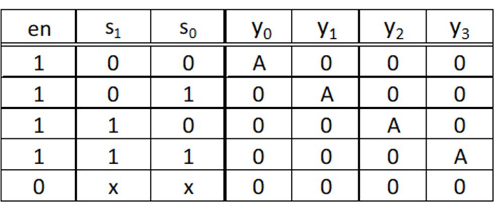
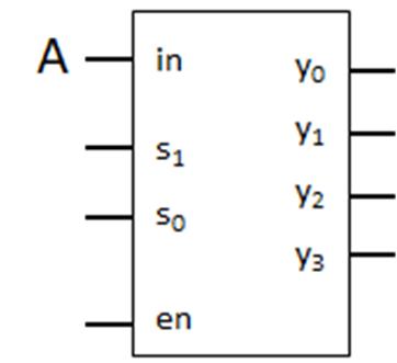
So, if the enable is 0 it doesn’t matter what the select lines are, the outputs will be 0. If the enable is 1 then notice that the output line corresponding with binary value formed by the selects is A, while all others are 0. For example, if s1,s0 = {0,1} then line y1 has the value of A and the others are 0.
The active low version of the de-mux flips everything. Fig. 5-39 (below) shows an active low 1:4 low de-mux and its associated truth table. Notice the inverting bubbles on the enable and outputs. So, the enable must be a 0 to activate the device. If the enable is 1, all the outputs are 1. If the enable is 0, then the corresponding output to the binary input on the select lines will be �� and all other outputs are 1. A de-mux is typically used in communication applications where there is a need for bi-directional signals. They are often used in tandem with a mux so it is possible to transmit or receive signals over the same path.
113
De‐multiplexor
Fig. 5‐37. Active high de‐mux with input A.
Fig. 5‐38. 1:4 de‐mux with active high enable.
5.7 Adders
Another black-box application is when we need to add two binary numbers. These “Adders” are used in every computing device and are the main component in a computer’s Arithmetic Logic Unit (ALU).
5.7.1 Adder operation
Suppose we want to add two 2-bit binary numbers:
We see that we will have two sum terms (the two 0’s in the answer for this example) and a carry term (the 1 in the answer). So, for 2-bit addition, we have three terms we need to calculate. We can create a truth table (below, left) for this in which we list every possible combination of each of our 2-bit binary numbers and the resulting sum and carry terms:
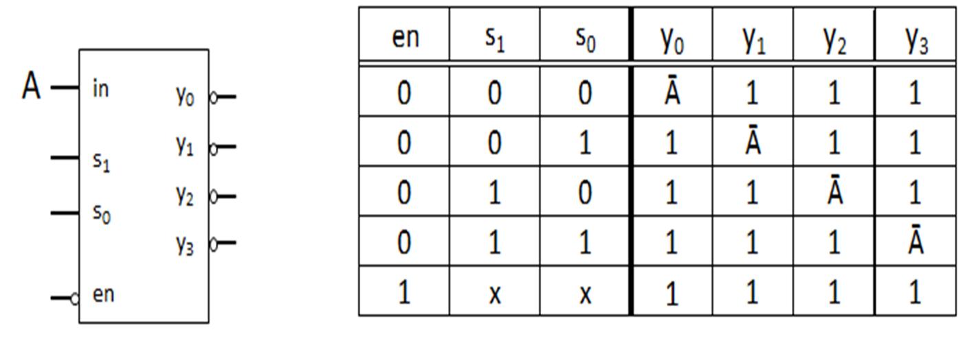
For two, 2-bit numbers, there are 16 possible combinations. We read this table as the addition of the 2-bit number formed by the first two columns (a1 and a0) with the binary number formed by the next two columns (b1 and b0). The resulting c, s1, and s0 are the addition results across each row. We see we would have to create three functions (one for each of c, s1, and s0) of four variables. This is very doable, however, not very useful in that it only allows us to do 2-bit addition! If I wanted to add two 16-bit numbers together (a common need in the computing world) the truth table would have 4,294,967,296 rows and would require solving 17 functions of 32 variables each! Obviously, this is not practical. Let’s examine how we would add two 4-bit numbers (below, left):
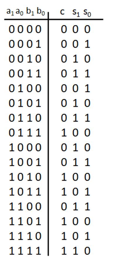
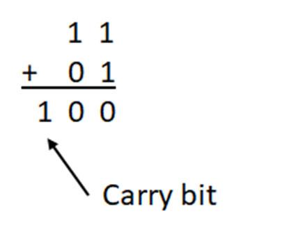
114
Fig. 5‐39. Active low 1:4 de‐mux and truth table.
The way we would solve this is to start from the right and compute each column. So, the far-right column adds 1 + 0. Its value is 1 with a carry of 0, as shown. Moving left one column, we add 1 + 1. This time the sum term is 0 and the carry is 1 because 1 + 1 = 2 which is 10 in binary. The next column adds 1 + 1 + 1 = 3 or 11 in binary so the sum term is 1 and the carry term is 1. In other words, we operate on the numbers one column at a time while carrying the results over from the previous column. We can mimic this action in hardware.
Notice, the far-right column will only have two bits to add, while the others will have three bits to add. We can create separate devices for these two cases. Let’s call the far-right addition for just two bits a “Half Adder” (HA). Fig. 5-40 provides a diagram of the HA device.
The HA has the two least significant bits a0 and b0 as input and outputs the least significant sum term, s0, and the first carry bit, c0. At this point we can make a truth table (left) for how this device functions:
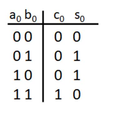
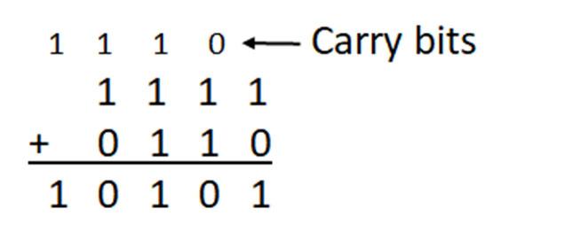
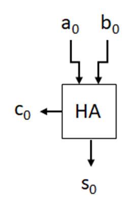
Once again, we read across each row adding the a and b bits to form the sum and carry bits. We can easily write down the equations for each of c and s0:
So, c is just the AND of the two inputs and s is the XOR of the two inputs.
The next devices for the columns in our addition problem require that we take into account the carry from the previous stage. This device is called a “Full Adder” (FA). Fig. 5-41 shows the diagram for the FA device.
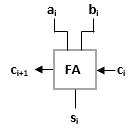
115
Fig. 5‐40. Diagram of a half adder device.
�� �� ∙�� �� �� ⊕��
Fig. 5‐41. Diagram for full adder device.
Once again, we have the a and b bits from the ith column of our addition problem, plus the carry from the previous column that we need to add. The truth table for this case is shown to the left:
With three input variables, we have eight rows, but still only two functions to calculate. Since each subsequent column will be calculated the same way, once we figure out the functions for the FA, we are done. We will simply cascade more FA devices until we reach the number of bits in our addition problem. The derivation of the function ci is given as follows:
Here we see that c is just all the combination of ANDing two variables at a time. Now let’s look at the s term:
Here we see that s is just the cascaded XOR of all three variables. While slightly more complicated than the HA, the FA is still easily implemented. By linking the HA and several FA modules, we can add any number of bits. Fig. 5-42 shows the HA and FA connections for the case of the 4-bit example.
We can then package the four devices all together and call it a 4-bit adder if we wanted. However, if we wanted to cascade two of the 4-bit adders to make an 8-bit adder, we couldn’t do that because we have no way to connect the carry from the last FA of one to the HA of the next to complete the 8-bit addition. Now we could make a separate device that can do that, but now we would have two devices to consider. It would be much more convenient to have a single device that we can adjust to do what we want. Well, there is. By replacing the HA with another FA, we get the diagram shown in Fig. 5-43.
116
Fig. 5‐42. 4‐bit adder using HA and FA devices.
By making the cin input a 0, the first FA acts just like a HA. However, we can now connect another set of four FAs to the cout output to form an 8-bit adder. Fig.
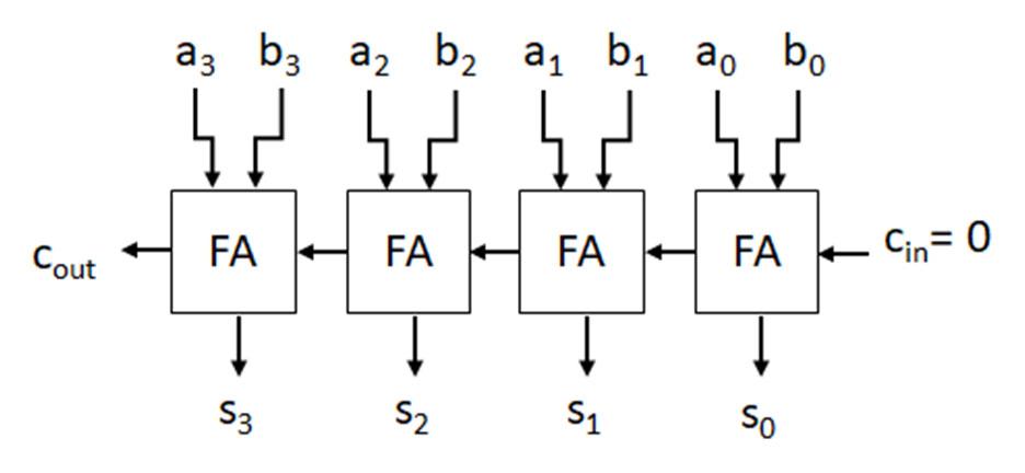
The adder structure is what’s known as a “Ripple-Carry” structure. The information entered into the right-most FA must ripple across each FA before reaching the left-most FA. The caveat is that this ripple-action takes time. For example, say we could actually implement the combinatorial logic to directly compute the addition of two 32-bit binary numbers. The addition, using combinatorial logic, would only take 6 nanoseconds (ns) to complete. The same addition of two 32-bit binary numbers using the Ripple-Carry structure adder would take approximately 64ns, a factor of 10 times longer! However, the combinatorial adder would take over 100 billion transistors to construct, while the ripple-carry adder only takes 380 transistors. The engineering compromises are speed versus size and complexity versus simplicity.
How do we calculate the delay of a ripple-carry adder? As mentioned above, we are looking for how long it takes the information to work its way across the FA devices. For example, let’s say we have a 4-bit adder where each sum operation takes 2ns and each carry operation takes 1.5ns. Fig. 5-45 (below) shows the ripple carry timing for this example.
From Fig. 5-45, the right-most FA takes 1.5ns to complete its carry operation. The next FA to the left must wait the 1.5ns before it can complete its operation. This is why it's carry out takes 3ns (1.5ns for the first FA + 1.5ns for the second FA). This repeats down the line with the next FA to the left needing 4.5ns before its carry out is a good value and the left-most FA takes 6ns before it has a good value. We also see that each sum operation adds the delay from the previous FA before the sum value is good.
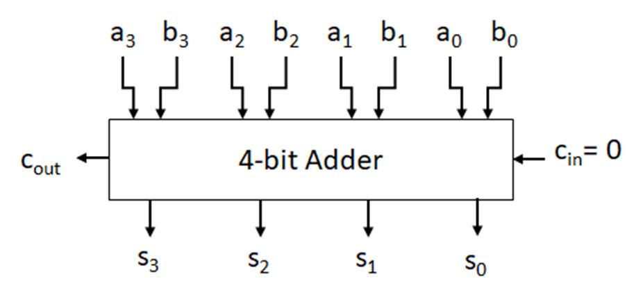
117
Fig. 5‐43. 4‐bit adder using FA devices.
5-44 shows a 4-bit adder black box
Fig. 5‐44. 4‐bit parallel adder digital component.
The figure also shows a second set of adders. Notice that the second set must wait for the first to complete before it can produce a good value. However, also notice that for the bottom, left-most FA both the time it took to travel across the top adders and then down and the time it took to go down then travel across the bottom adders is identical, 6.5ns. If all the delay times are identical in the adders, we just need to pick a path from the top, right-most FA to the bottom, left-most FA and add up the delay times to get the overall delay through the adders.
5.7.2 Subtraction with Adders
Recall, we are able to subtract one binary number from another using the 2’s complement representation. Furthermore, we showed how we can first convert a binary number into a 1’s complement form by flipping the bits of the binary number and then adding 1 to the least significant bit (LSB). By combining the Adder with a set of inverters, we can perform 2’s complement and, therefore, implement subtraction with our device.
The process of flipping the bits to perform a 1’s complement operation is implemented by inverting the bits of the binary number as shown in the figure. Let a binary variable �� ��
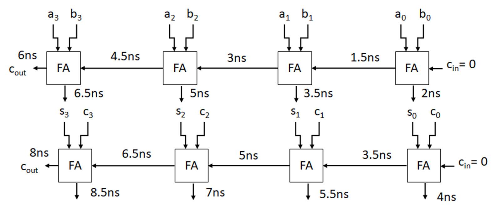
then to take the 1’s complement of (B) is shown in Fig. 5-46.
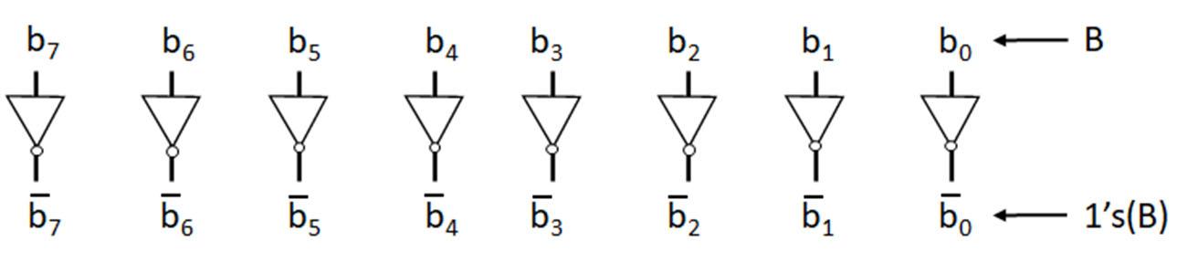
To complete the 2’s complement operation we need to add 1 to the LSB, however, our adder circuit gives us the “carry in” input on the LSB of the adder so we can complete the 2’s complement.
Now, to perform the subtraction of a binary variable �� �� �� �� �� �� �� �� �� by our variable B we simply add A + 2’s(B). The diagram to do this is shown in Fig. 5-47.
118
Fig. 5‐45. 4‐bit ripple carry timing example.
�� �� �� �� �� ��
��
Fig. 5‐46. 1’s comp diagram for B.
5.7.3 More Fun with Adders
We can multiply by integers using a shifting property of binary multiplication and an adder. Recall, when we multiply by a number that is a power of two (i.e., 1,2,4,8,16,...) we shift the multiplicand by the power of two. For example, let a 4-bit binary number C={1011}, if we multiply C by 2 we get:
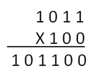
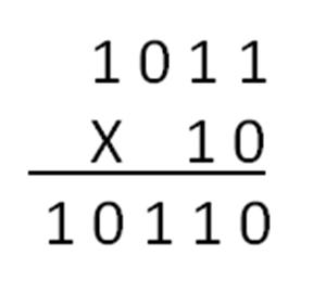
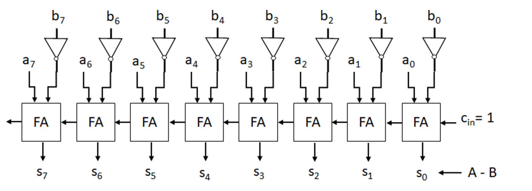
Multiply by 4 we get:
With 2 = 21 and 4 = 22, we see that when we multiply by 2, we simply shifted the bits of C to the left by one position and filled in the LSB with a 0. When we multiply by 4, we shifted C by two positions and filled in with two 0’s. We will see in a later chapter how we can perform this shifting property in hardware.
Let’s say that we want to multiply C by the integer 5. Five is not a power of two, so we cannot directly shift C, but we can rewrite 5�� 4�� �� . We can shift 4C since 4 is a power of 2. We then add C to 4C to get the desired 5C. Using the 8-bit adder we used previously, the diagram to perform 5C is shown in Fig. 5-48.
119
Fig. 5‐47. 8‐bit parallel adder circuit to compute A‐B.
Note: We’ve padded extra 0’s to C to make it 8-bit. In the figure, the right input to each FA is for the 4C terms, while the left input for each FA is for the C terms. The output is 5C.
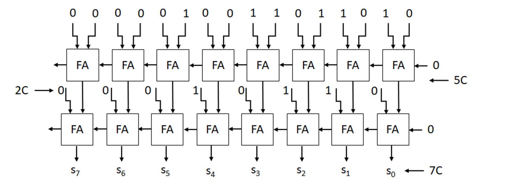
Let’s say we want to calculate 7C. We can rewrite 7�� 4�� �� 2�� . Note that we have the 4C + C terms in the figure above. To finish 7C we only have to add the result of 4C + C with 2C as shown in Fig. 5-49.
We could have also rewritten 7�� 8�� �� . In this case, we would not have needed the second set of adders, but we would have used the subtraction technique we saw previously using a row of inverters to perform the 2’s complement of C.
Finally, let’s combine all these to find �� �� 5�� , where �� 00�� �� �� �� �� �� (note the 2 padded 0’s) and �� 00001011 . The diagram for this operation is shown in Fig. 5-50 (below).
We can now perform a host of different operations using adders, inverters, and shifting variables.
120
Fig. 5‐48. Parallel adder circuit modified to compute C + 4C.
Fig. 5‐49. Parallel adder circuit modified to compute C + 4C + 2C.
In real computing systems, we usually are restricted in the space we have to put components. It is advantageous if we can get multiple types of operations using the same device. In the figure above, we see that we need one set of adders for addition and another set for subtraction. If we could make one set of adders operate as either addition or subtraction by telling it what to do (in other words, using a control bit to switch from addition and subtraction) we could save space in our computer. It turns out, we can use an XOR gate as a selectable inverter. Recall the truth table for an XOR gate:
If we use the X input as our control variable, if X = 0 and then compare Y with the output of the XOR gate, we see that they are equal, so the XOR is acting as a buffer. However, if X = 1 then the XOR output is the inverse of Y so the XOR gate is acting as an inverter. We can use this property. Let sub be a control line such that if sub = 1, then subtract binary variables A - B. If sub = 0 then add A + B. Fig. 5-51 below shows the diagram for this operation.
So, by simply adding a row of XOR gates we can select if we want to add or subtract using the adder.
121
Fig. 5‐50. Parallel adder circuit modified to compute A‐5C.
5.8 Programmable Logic Arrays
As our systems become more complex, it is necessary to have the ability to redesign the logic without having to completely rebuild the hardware. One of the devices that makes this possible is programmable logic. With programmable logic we design and redesign combinatorial functions simply by reprogramming the chip with no change to the hardware layout. There are many forms of programmable logic, so in this chapter we will use the generic term of Programmable Logic Array (PLA) to refer to this combinatorial logic class of programmable devices.
5.8.1 Programmable Types and Conventional Symbols
Early PLA’s allowed for a 100 or so gates. For many cases, 100 gates is more than enough to implement any combinatorial function a design needed. However, as it was discovered how useful the devices are, it became apparent that larger devices were needed and a more complex PLA was created that was able to accommodate 1000’s of gates. A modern Field Programmable Gate Array (FPGA) may have 10,000 to 1,000,000 gates. The FPGA has made it possible to build massively complex and parallel systems yet make corrections without changing the hardware layout.
There are two symbol conventions used here. Within the structure of the PLA, the inverted and non-inverted values of the inputs are generated. This eliminates the need to bring in both signals to the chip. This is done by both buffering and inverting the input such that the timing remains the same for the signal. To simplify the PLA diagram, the inverter and buffer are combined into a single device as shown in Fig. 5-52 below.
122
Fig. 5‐51. Parallel adder/subtractor diagram.
The other convention used is that the number of connections to the OR and gate inside the PLA are unknown and can be changed. A new device called a “Wired-OR” and a “Wired-AND” are used such that the number of connections to the OR AND gates can be selected. The technology used is different than was discussed in CMOS, and is outside the scope of this course, but we will use the technology to our advantage! We will simply show the OR and gates as a single input (shown in the figure below) By connecting a signal to the input line it is considered as an input to the gate.
5.8.2 OR/AND PLA
The structure of the PLA is straight forward. It consists of an input array where the input variables are represented in both the inverted and non-inverted form which are then connected (or not connected) to a set of Wired-OR gates. The OR gates then form an output array that are connected to the Wire-AND gates that are then output from the PLA. This type of PLA is called an OR/AND PLA since we first pass the signals through the OR gates then through the AND gates. We indicate a connection to a Wired-OR/AND gate with a connection dot. Fig. 5-53 (below) shows the OR/AND PLA.
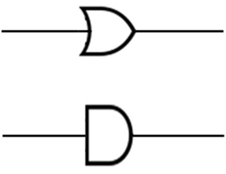
We see that the output of the OR gates are POS terms which are then ANDed together form the outputs. The OR/AND PLA, therefore, is using the POS form to construct the combinatorial function.
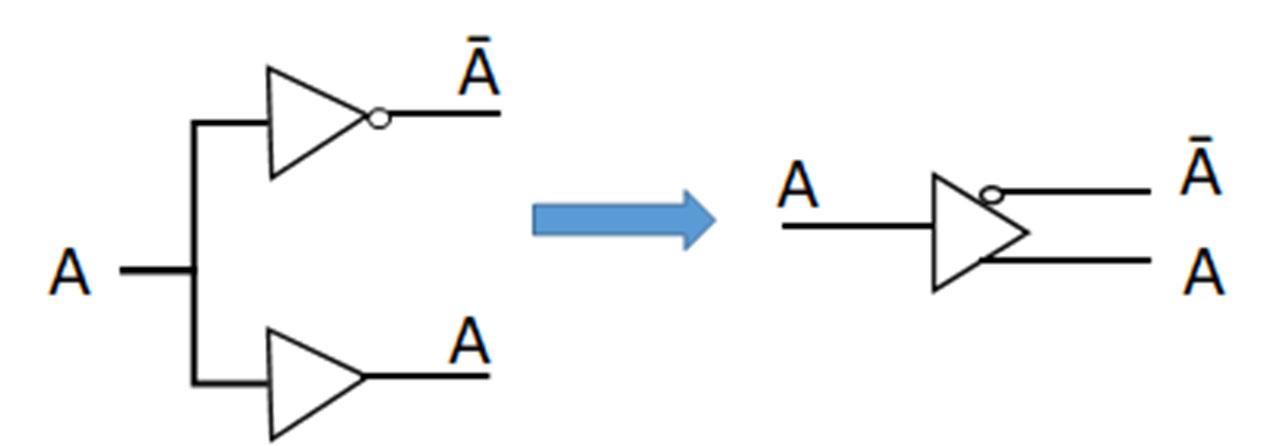
123
Fig. 5‐52. Buffer and inverter notation.
The AND/OR PLA is nearly the same as the OR/AND PLA except that the AND gates are first then the OR gates. Otherwise, the same input array and output array are used to form the combinatorial functions. Fig. 5-54 shows the AND/OR PLA example for a 3-variable function F.
In this case, we see that the output of the AND gates produce the SOP terms and the output is the sum of the products, therefore, it uses the SOP form to implement the combinatorial function. We see in this diagram that the output, F, is the function:
124
Fig. 5‐53. OR/AND PLA multi‐function implementation example.
5.8.3 AND/OR PLA
Fig. 5‐54. AND/OR PLA function implementation example.
�� ������ ������ ������ ������
5.8.4 PLA’s with minterm and maxterm functions
We see above that the AND/OR PLA produces the product terms of an SOP function, and if we force each term to contain all the variables in the function, we have a Canonical SOP function. We have previously seen that Canonical SOP terms are what we call the minterms of the function. We can use this same idea with a PLA where we force connections (either inverted or non-inverted) to all the input variables of an AND/OR PLA and we end up producing the minterm representation of our function. This is illustrated in Fig. 5.55.
Of course, if you connect to all the minterms the function F = 1. Assuming you don’t want your function to be 1, you would only connect the needed minterms to the output OR gate. By simply selecting a different set of connections, we can form multiple output functions all represented by the minterms.
The OR/AND PLA produces the maxterm representation of the function. We can form a similar PLA as the minterm PLA above for the maxterm PLA, in Fig. 5-56 below.
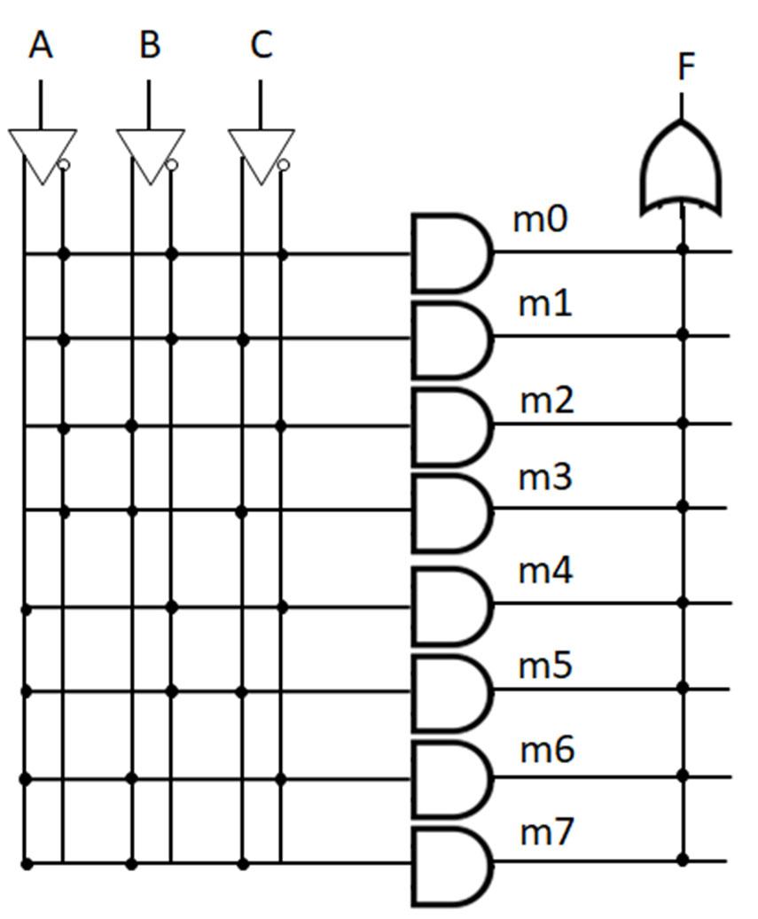
125
Fig. 5‐55. AND/OR PLA function implementation example (F = 1).
Note, however, that the maxterms are reversed from that of the minterms for the same input connection matrix. This makes sense by simply remembering that the minterm is the inverse of the maxterm. By DeMorgan’s Law we know that the input variables will also invert. This can sometimes cause confusion, but if we remember that the maxterm function flips the inputs, we can remember which maxterm we are using.
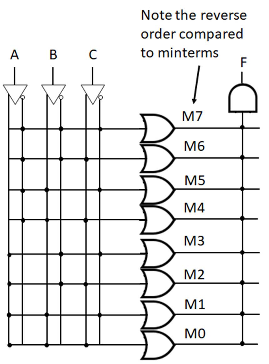
5.8.5 Implementing simplified functions in a PLA
We see above that if we connect all the variables to each of the input array OR AND gates we end up with a Canonical Form. However, when we simplify the function, we end up with terms missing variables. We can implement these within a PLA by simply not connecting a variable to the input side OR AND gates. Let’s illustrate this in an example.
To start, let’s construct an AND/OR PLA for the function �� ���� 0,1,4,7 . We see the function is in minterm form so we can directly implement the function with an AND/OR PLA shown in Fig. 5-57 (below).
126
Fig. 5‐56. OR/AND PLA function implementation example (F = 0).
Now, let’s simplify the function using a K-Map:
The function simplifies to �� ���� ���� ������ . The term ABC is minterm 7 (m7) so we know how to create that term in a PLA, However, the other two terms only have two variables so we need to only connect those two variables in the PLA. The function is implemented in Fig. 5-58.
We see that the first line only connects to A and B terms (both inverted) and does not connect to C to form the first term in the function. Likewise, for the second term we don’t use A but connect to B and C. This PLA will produce the same output as the previous PLA that was constructed using the minterms. Note, however, the second PLA uses one less AND gate in addition to fewer connections. So, by reducing the function, we can get more functions on the PLA and reduce the amount of programming, which is a frequent cause of errors.
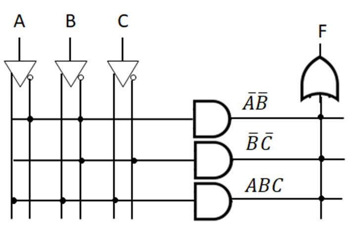
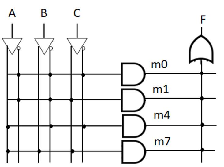
We can then add to this example by adding a second function �� ���� 0,1,3,4 . Again, reducing the function we get the K-map:
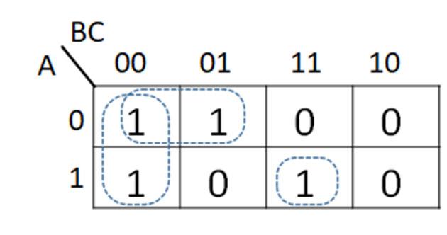
127
Fig. 5‐57. Minterm expression implementation using an AND/OR PLA.
Fig. 5‐58. AND/OR PLA implementation for the simplified function F.
The function reduces to �� ���� ���� . The PLA already has the ���� term so we only need to generate ���� . The function is implemented in Fig. 5-59.
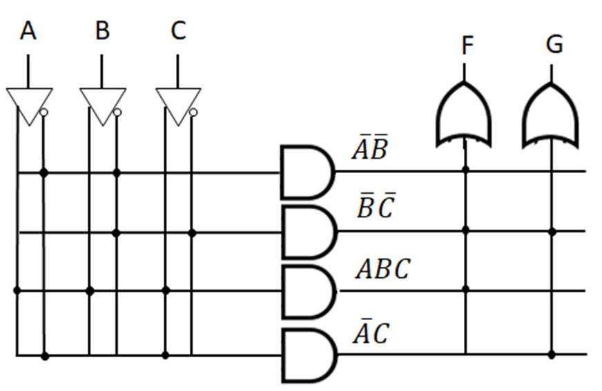
This is a simplistic example which illustrates how we can use PLAs to implement functions in a very compact form.
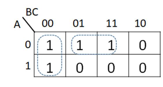
128
Fig. 5‐59. AND/OR PLA multi‐simplified function implementation.
Chapter 6: Memory Elements
Chapter 6 Learning Goals
Understand and implement simple digital storage devices
Chapter 6 Learning Objectives
Define the properties of a bi-stable feedback latch
Define the operation of NOR SR and NAND SR latches
Define the operation of a D latch
Define the operation of a flip-flop
Define the operation of a D, SR, JK, and T flip-flops
Construct timing diagrams for latches and flip-flops
Construct Parallel Load and Shift Registers
Construct a ring counter to perform standard operations
Construct a RAM memory cell
Construct a RAM Chip
Construct a ROM Chip
Understand the effective size of a RAM/ROM generic circuit
129
In the previous chapters, digital circuit design has been examined for a number of digital components and digital logic techniques to perform specific logic operations and to manipulate logic functions for their implementation. This digital circuit design utilizes combinational logic gates and digital components that take present time inputs to perform the determined operation and produce a present time output. In this chapter, digital components and memory components are considered that can be used to store data values and access them as needed. Several memory components are introduced with logic and signal representations and their application in digital circuits.
6.1 Latch
The latch is the initial memory component that is examined. A latch is a logic element that follows data variations at the component input and transfers these variations to an output line. Fig. 6-1 shows a diagram of a basic latch.
The operation of latch devices is characterized by two properties: 1) Latches are transparent devices such that the output Q follows the input D (as given above) at least part of the time and 2) Latches are bistable circuits, where the device outputs Q and Q’ are complementary values such that when Q = 0, Q’ = 1 and when Q = 1, Q’ = 0 in order to maintain a stable circuits.
6.2 Set (S) Reset(R) Latch
There are several types of latches. The Set (S) Reset (R) latch has S and R as the inputs and Q and Q’ as the outputs, with S referring to setting/forcing the output Q = 1 and R referring to resetting/forcing the output Q = 0. Fig. 6-2 gives the black box diagram of an SR latch.
130
Fig. 6‐1. Diagram of a basic latch.
Latch Input Output D Q Enable EN Q’
The SR latch has two implementations: a) NOR SR latch and b) NAND SR latch.
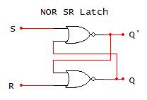
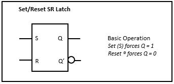
6.2.1 NOR SR Latch
The NOR SR latch uses two NOR gates with cross-coupled outputs that are fed as one of the inputs to the other NOR gate. S and R provide the second input to each NOR gate, respectively. The outputs of the NOR gates are labeled as Q and Q’. A NOR SR latch is shown below with its truth table. Fig. 6-3 below presents the derivation of the NOR SR latch based on breaking apart the two NOR gates and applying the SR input combinations. The NOR gate truth table is provided in the figure as a reference.
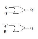
131
Fig. 6‐2 Black box diagram of an SR latch.
Disassembled and Labeled NOR SR Latch
NOR Gate Truth Table NOR SR Latch Truth Table A B �� �� S R Q 0 0 1 0 0 Q (Hold) 0 1 0 0 1 0 (Reset) 1 0 0 1 0 1 (Set) 1 1 0 1 1 Not Used
Fig. 6‐3. NOR SR latch, truth table and labeled disassembly.
The NOR SR latch is disassembled and labeled above with the individual NOR gates to derive each entry in the NOR SR latch truth table. For each SR input value combination, the inputs and outputs for each of the two NOR gates are determined. A property of the two input NOR gate is that if either of the inputs is a logic 1, then the output of the NOR gate is 0. For the case when S = 0 and R = 1, the NOR gate with inputs R and Q’ has an output of Q = 0 since at least one of the inputs is 1. With S = 0 and Q = 0 (as determined), then Q’ = 1 from the truth table of the NOR gate. Thus, when S = 0 and R = 1, then Q = 0 and Q’ = 1, which is the reset condition based on forcing the output Q = 0.
6.2.2 NAND SR Latch
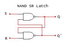
A second, less common, implementation of the SR latch uses cross-coupled NAND gates instead of NOR gates. The configuration of the NAND SR latch is shown below with its truth table. Note the orientation of the inputs S and R and the outputs Q and Q’. Fig. 6-4 shows the derivation of the NAND SR latch truth table entries based on the disassembled and labeled NAND gates (below) using the same process as for the NOR SR Latch. For this derivation, the NAND gate truth table is provided as a reference. The truth table highlights if one of the inputs is a 0, then the output of the NAND gate is a 1.
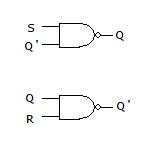
132
Disassembled and Labeled NAND SR Latch
NAND Gate Truth Table NAND SR Latch Truth Table A B �� ∙�� S R Q 0 0 1 0 0 Not Used 0 1 1 0 1 1 (Set) 1 0 1 1 0 0 (Reset) 1 1 0 1 1 Hold (Q)
Fig. 6‐4. NAND SR latch, truth table and labeled disassembly.
6.2.3 D Latch
The D latch is a special case of the NOR SR latch with D and D’ replacing S and R, respectively, in the NOR SR latch configuration. The D latch truth table is shown in Fig. 6-5, with D = Q. The disassembled and labeled NOR gates are shown for the derivation of the truth entries. When D = 0, D’ = 1 yielding Q = 0 and Q’ = 1. When D = 1, D’ = 0 giving Q’ = 0 and Q = 1. As a special case of the NOR SR Latch, D = 0 corresponds to S = 0 and R = 1 to produce Q = 0, and D = 1 corresponds to S = 1 and R = 0 to generate Q = 1. The D latch is the most commonly used latch component in digital systems.
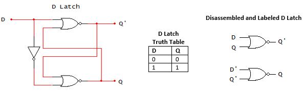
Latches are memory elements that use binary variable inputs in the form of digital signals. Latches may or may not use enable signals. An enable signal, when active, allows the latch device to function according to its truth table, and, when inactive, maintains the current output of the latch without regard to changes to the latch input(s). The enable signal may be a periodic clock signal that can be used to coordinate the flow of binary variable data within digital systems. The previous presentations of the NOR SR, NAND SR, and D Latches do not include enable signals.
6.3 Clocked Latches as Memory Elements
In this section, enable signals are integrated into the SR and D latches presented in the previous section to control data flow in digital systems. The SR and D latch truth tables with signal examples are presented.
6.3.1 Clocked SR Latch
Conventionally clocked SR latches use the NOR SR latch configuration. The usage of clocked SR latches are based on NOR SR latch configurations in this textbook. Fig. 6-5 below gives the clocked NOR SR latch with ∅ denoting the enable signal. ∅ is ANDed with S and R to provide the latch inputs S∅ and R∅. If ∅ = 0, then S∅ = 0 and R∅ = 0, which yields the hold (Q) output of the NOR SR latch. S and R can change but do not impact the output Q. If ∅ = 1, then S∅ = S and
133
Fig. 6‐4. D latch, truth table and labeled disassembly.
R∅ = R, which gives the normal NOR SR latch truth. The clocked NOR SR latch truth is presented with ∅ ∅ controls when the data inputs S and R can update the output Q and when the output Q is maintained (held) for use with other operations in digital circuits.
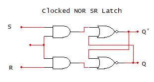
A timing diagram is also presented in Fig. 6-5 showing the periodic enable signal (∅) with input signals S and R. The output Q is determined based on applying the truth table to these signals. Notice that the rising and falling positions of the enable signal (∅) are labeled to highlight the high (1) and low (0) portions of the enable signal. The output Q is determined based on the enable signal going from left to right. At the initial leftmost portion of the enable signal (∅) (see a timing diagram), ∅ = 0, which yields the hold condition (Q keeps its current value). Since Q is unspecified with an initial value, Q must be specified with an initial value. In the timing diagram examples presented throughout this chapter, initial values are specified as Q = 0. The output Q = 0 is held (maintained) as long as ∅ = 0. When ∅ transitions from 0 (low) to 1 (high) (see b), the truth table for the SR latch is applied to the S and R signals to determine the value Q while ∅ = 1 (see a in the timing diagram). S transitions to 1 with R being 0, resulting in Q = 1 (set). Then, S transitions to 0 with R being 0, yielding Q to be held (maintained with current value of Q = 1). The values of S
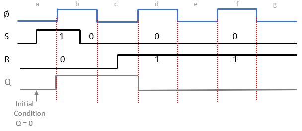
134
Timing Diagram Example for Clocked SR Latch
Fig. 6‐5. Clocked SR latch, truth table and timing diagram example.
Clocked NOR SR Latch Truth Table ∅ S R Q
0 0 Hold (Q)
0 1 0 (Reset)
1 0 1 (Set)
Not Used 0
(Q)
1
1
1
1 1 1
‐ ‐ Hold
Don’t
∅
‐ denotes a
Care
and R do not change again while ∅ = 1, so Q maintains it current value. When ∅ transitions from ∅ = 1 to ∅ = 0 (see c), the SR latch holds its current output (Q = 1 in this case) until ∅ transitions to 1 again. When ∅ transitions from ∅ = 0 to ∅ = 1 (see d), S = 0 and R = 1, which gives Q = 0 (reset). S and R do not change during the period when ∅ = 1, so Q = 0 is held. When ∅ transitions from ∅ = 1 to ∅ = 0 (see e), Q is held (Q = 0). When ∅ transitions from ∅ = 0 to ∅ = 1 (see f), S = 0 and R = 1, yielding Q = 0 (reset). S and R have constant values while ∅ = 1, keeping Q = 0. When ∅ transitions from ∅ = 1 to ∅ = 0 (see g), Q is held (Q = 0).
The clocked SR latch has logic symbols. The symbols shown below in Fig. 6-6 use clk for the enable ∅ signal with the input signals S and R and the output signals Q and Q’. When the enable signal ∅ does not have a bubble by the symbol, the clocked SR latch behaves as presented in the previous example. If there is a bubble next to the clk label, then ∅ is inverted going to the AND gates to provide the condition that ∅ must be 0 for the SR latch to behave normally according to the truth table. When ∅ = 1, ∅’ = 0 making the outputs of the AND gates 0s, which is the hold condition for the SR latch (Q keeps its value regardless of changes to S and R). When the latch can change the output value when ∅ = 1 (no bubble on the latch symbol next to clk), the latch is referred to as level high. When the latch can change the output value when ∅ = 0 (bubble on the latch symbol next to clk), the latch is referred to as level low. A bubble is used to designate the NOT (or invert) operation logically.
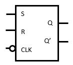
6.3.2 Clocked D Latch
The clocked D latch configuration (level high) with its truth table is given in Fig. 6-7 below. Again, ∅ represents the enable (or clock) signal. A timing diagram for the level high clocked D latch is shown below. In the timing diagram, an assumed value of Q = 0 is given (see a in the timing diagram below). With an active high clocked D latch, when ∅ = 0, Q keeps its present value (assumed to be Q = 0). When the enable transitions to ∅ = 1 (see b), the D latch has its normal truth table behavior (D = Q). So, the output Q follows the value of the input D. When the enable (clock) transitions to ∅ = 0 (see c), Q maintains its value from prior to the enable transition (Q = 1 in this case). When the enable transitions to ∅ = 1 (see d), the D latch has its normal truth table behavior (D = Q). When the enable (clock) transitions to ∅ = 0 (see e), Q maintains its value
135
Level High Level Low
Fig. 6‐6. Clocked SR latch symbols.
from prior to the enable transition (Q = 0 in this case). When the enable transitions to ∅ = 1 (see f), the D latch has its normal truth table behavior (D = Q). When the enable (clock) transitions to ∅ = 0 (see g), Q maintains its value from prior to the enable transition (Q = 0 in this case).
‐ denotes a Don’t Care
Fig. 6-8 shows a level low clocked D latch logic symbol, associated clocked D latch gate configuration, and timing diagram using the level low clocked D latch. Again, the level low clocked D latch has a bubble (NOT) on the symbol and requires ∅ = 0 (level low) for the D latch to have its normal truth table operation. With ∅ = 1, the inputs to both NOR gates become 0s, which is the hold condition (based on the NOR SR latch that the D latch is derived).
In the timing diagram for the active low clocked D latch in Fig. 6-8, no assumed value of Q is needed because when ∅ = 0 (see a), the D latch has its normal truth table behavior (D = Q). Q keeps its present value (assumed to be Q = 0). When the enable transitions to ∅ = 1 (see b), Q keeps its present value (in this case Q = 0). When the enable (clock) transitions to ∅ = 0 (see c), the D latch has its normal truth table behavior (D = Q). When the enable (clock) transitions to ∅ = 1 (see d), Q maintains its value from prior to the enable transition (Q = 0 in this case). When
136
Timing Diagram Example for Level High D Latch
Fig. 6‐7. Clocked level high D latch, truth table, and timing diagram example.
∅
0
Clocked D Latch Truth Table
D Q 1 0 0 1 1 1
‐ Hold (Q)
∅
the enable transitions to ∅ = 0 (see e), the D latch has its normal truth table behavior (D = Q). When the enable transitions to ∅ = 1 (see f), Q maintains its value from prior to the enable transition (Q = 1 in this case). When the enable (clock) transitions to ∅ = 0 (see g), the D latch has its normal truth table behavior (D = Q). Thus, the enable level has an impact on how the input to the latch (D) impacts the output Q. Active high and active low enabled clocked D latches are both commonly used digital components, so attention must be given to the device used in digital circuit implementation.
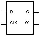
6.4 Flip Flop
The most commonly used storage element in digital systems is a flip flop. A flip flop is a nontransparent latch that is controlled by an enable or clock signal. In the operation of a flip flop, the output Q is not related to the present input. There are two types of flip flops: master-slave and edge-triggered flip flops. Both flip flop types operate with the same truth tables. The edgetriggered flip flop is implemented using a NAND SR latch with additional NAND gates. The master-slave flip flop configuration uses two cascading clocked latches with the output of the first latch fed as the input to the second latch. The input to the first latch and the output of the second latch provide the input and output for the flip flop. The first and second clocked latches use
137
Timing Diagram Example for Level Low D Latch
Fig. 6‐8. Clocked level low D latch, truth table, and timing diagram example.
Level Low D Latch Truth Table ∅ D Q 0 0 0 0 1 1 1 ‐ Hold (Q) ‐ denotes a Don’t Care ∅
opposite levels of the enable/clock signal. The figure master-slave flip flop configuration is shown in Fig. 6-9 below with the signal A as the input, Q as the output, and M and S denoting the master and slave clocked latches, respectively. ∅ is the enable or clock signal provided to both latches. Note in this configuration that M is a level high latch and S is a level low latch.
The behavior of the master-slave flip flop is based on the enable/clock signal when M is enabled (active), with S enabled (active) on the opposite level of the enable/clock signal. Using the configuration above, when ∅ = 1, M is active. The output of M follows the input A based on the truth table for the clocked M latch. When M is active, the inverter for ∅ makes ∅’ = 0, causing S to hold its current output Q. Changes in the input to S (output of M) do not update the output for S. An illustration of this process is given in Fig. 6-10 below.
Using the master-slave configuration above, when ∅ = 0, S is active. The output of S follows the input provided by the output of M, applying the truth table for the clocked S latch. When S is active, M holds its current output (not labeled on the diagram above). This process is illustrated in Fig. 6-11. Changes in the input A do not update the output of M, so that the output of the flip
138
Input Output A M S Q ∅ ∅ S M
M = Master Latch S = Slave Latch
Fig. 6‐9. Master‐slave flip‐flop configuration.
Input Active Hold Output A M S Q ∅ ∅ M S
M = Master Latch S = Slave Latch
Fig. 6‐10. Master latch active receiving the input A with slave latch in a hold condition.
flop (output of S) does not follow the input A. Thus, the output of the flip flop Q is determined explicitly by the output of M when ∅ makes the transition from 1 to 0 (last point in time when M is active receiving the input A to obtain the output of M AND the point in time when S becomes active receiving the constant output from M to determine Q). Another way of interpreting the operation of the flip flop is that the transition of value in ∅ is the only time that the output Q of the flip flop directly relates to the input A. Flip flop truth tables are defined using this enable/clock transition point to define the output Q, denoted as Q*, for a given flip flop input.
6.4.1 Rising and Falling Edge Enable/Clock Transitions
The description of flip flop operation is based on the enable/clock transition to determine the flip flop input and output truth table determination. There are two types of enable/clock transitions. The first transition type is high-to-low or falling edge. The master-slave flip flop configuration presented in the previous section is based on M active (S hold) when ∅ = 1 and S active (M hold) ∅ = 0. providing the falling edge enable/clock transition for the flip flop input and output (Q*) truth table values.
The second transition type is low-to-high or rising edge. The master-slave flip flop configuration in this case is based on M active (S hold) when ∅ = 0 and S active (M hold) ∅ = 1, providing the rising edge enable/clock transition for the flip flop input and output (Q*) truth table values. An example of the master-slave configuration for a rising edge flip flop is shown in Fig. 6-12 below.
139
Input Hold Active Output A M S Q ∅ ∅ M S M = Master Latch S =
Slave Latch
Fig. 6‐11. Slave latch active receiving the output from the master latch with the master latch is in a hold condition not being updated with the incoming input A.
The next section presents the logic symbols and truth tables for D, SR, JK, and T flip flops. The enable/clock signals (rising or falling edge) are designated on the logic symbols.

6.5 Flip Flop Definitions
Based on the master-slave configuration and rising and falling enable/clock variations, D, SR, JK, and T flip flops are defined with logic symbols and truth tables.
6.5.1 D Flip Flop
The D flip flop (DFF) uses cascaded M and S clocked D latches in its implementation. D is the input for the master latch M, and Q and Q’ are the outputs of the slave latch S in specifying the DFF. The logic symbols for the DFF rising and falling edge implementations are shown in Fig. 613 below. Note that clk is used to denote the enable/clock for a clocked D latch, and > denotes the enable/clock signal for a flip flop (FF). > with no bubble denotes a rising edge DFF, and > with a bubble denotes a falling edge DFF. The enable/clock signal ∅ is shown for the respective masterslave rising and falling edge configurations. The truth tables for both implementations of the DFF are the same, with input D and output Q* (after the clock transition). The only difference interpreting the truth tables for the rising and falling edge DFFs is the transition point in ∅ (lowto-high transition for rising edge and high-to-low transition for falling edge).
140 Input Active Hold Output A M S Q ∅ M S ∅ Rising Edge
M = Master Latch S = Slave Latch
Fig. 6‐12. Rising edge configuration for a master‐slave flip‐flop.
6.5.2 SR Flip Flop
The Set Reset flip flop (SR FF) is based on a master-slave setup using M and S as clocked NOR SR latches with rising and falling edge enable/clock signal configurations. The rising edge symbol for the SR FF and its truth table are shown in Fig. 6-14 below. The SR FF has the same truth table entries as the NOR SR latch, but the output Q* refers to the output of the SR FF based on the SR input values at the rising edge ∅ transition.
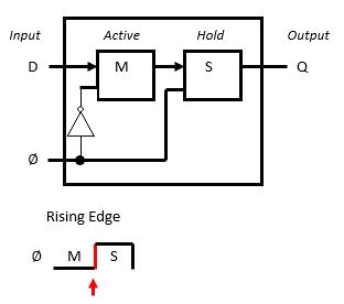
141 Rising Edge D Flip‐Flop Falling Edge D Flip‐Flop D Q D Q > Q’ > Q’
* after rising edge transition
* after falling edge transition
Fig. 6‐13. Rising and falling edge configurations for a D flip‐flop.
D Q* 0 0 1 1 D Q* 0 0 1 1
Rising Edge
6.5.3 JK Flip Flop
The JK flip flop (JK FF) derives its name from Jack Kilby and is the most versatile of the flip flops. Its functionality is very similar to the SR FF, with J and K corresponding to S and R, respectively, except that JK = 11 represents toggling the present output Q rather than “not used” in the case of the SR truth table. The JK FF logic symbol and truth table are shown in Fig. 6-15 below for the rising edge case.
6.5.4 T Flip Flop
The toggle (T) flip flop (TFF) uses the input T to either maintain the present output Q of the FF (T = 0) or to toggle the present output of the FF (T = 1). The symbol for a rising edge TFF and truth table are shown in Fig. 6-16 below.
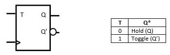
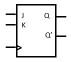
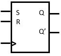
142
Set/Reset (SR) Flip Flop
Fig. 6‐14. Rising edge SR flip‐flop symbol and SR flip‐flop truth table.
JK Flip Flop
Fig. 6‐15. Rising edge JK flip‐flop symbol and JK flip‐flop truth table.
Toggle (T) Flip Flop
S R Q* 0 0 Hold (Q) 0 1 0 1 0 1 1 1 Not Used J K Q* 0 0 Hold (Q) 0 1 0 1 0 1 1 1 Toggle (Q’)
Fig. 6‐16. Rising edge T flip‐flop symbol and T flip‐flop truth table.
6.5.5 Example Timing Diagrams
In this section, signal diagrams (timing diagrams) examples are presented for clocked latches, flip flops for different enable/clock configurations, shown in Fig. 6-17. The first example below presents a periodic clock signal (clk, same as ∅) with a D input signal that is applied to all of the devices. The first (top) device is a level high clocked D latch. The symbol includes clk with no bubble to indicate a clocked latch and is active when the enable/clock signal is high and is in a hold condition when the enable/clock signal is low. Going through the timing diagram for the output Q from left to right. In a, the initial low clk value represents a hold condition to maintain the present output Q. Since Q has not been specified, an initial condition (Q = 0 in this case) is given. Q = 0 is maintained while clk is low. In b, clk is high so the D latch truth table relationship Q = D is applied. Q follows the value of the input D. The last value of D while clk is high is D = 0 (marked with an X on the D signal). In c, clk is low so that the Q is constant (Q = 0), holding the last value from D while the latch was active (D = 0). In d, clk is high, with Q = D. In e, clk is low with Q = 1 (D = 1 is the last value of D while the latch was active). In f, clk is high, with Q = D. In g, clk is low with Q = 1 (value of D held after clk made the 1 to 0 transition).
The second device (bottom device) is a rising edge DFF. The symbols contains a > and there is no bubble. In a, a rising edge transition has not occurred yet, so an assumed value of Q is needed (Q = 0). In b, there is a rising edge transition between a and b. D = 1 at that rising edge transition time, so Q = 1. From the previous discussion of flip flops, at enable/clock times other than the transition, the output Q is constant with its value prior to the transition and constant with its value after the transition. In c, Q is held constant (Q = 1). In d, the value of D at the transition from c to d (D = 0) is passed to the output Q (Q = 0) and held constant until the next rising edge transition. The next rising edge transition occurs between e and f. At this transition time D = 0, so Q = 0 after the transition time until the next rising edge in clk.
The final device shown in the timing diagram is a falling edge DFF (> with a bubble). In a falling edge DFF, the high-to-low enable/clock transitions are when the output Q* reflects the truth table value of the FF input D (value of D immediately before the enable/clock transition). In a, the FF output has an assumed value (Q = 0 in this case) because no falling edge transition has occurred yet. In b, the assumed output value Q = 0 is maintained until the next falling edge transition. In c, the falling edge transition occurred between the end of b and the start of c. D = 0 at that transition position, so Q = 0 after the enable/clock transition (Q* = 0 for D = 0 in the DFF truth table). In d, clk is high, which maintains (holds) the current value of Q (Q = 0). In e, the falling edge transition occurred between the end of 4 and the start of 5. D = 1 at that transition position, so Q = 1 after the enable/clock transition (Q* = 1 for D = 1 in the DFF truth table). In f, clk is high, which maintains (holds) the current value of Q (Q = 0). In g, the falling edge transition occurred between the end of f and the start of g. D = 1 at that transition position, so Q = 1 after the enable/clock transition (Q* = 1 for D = 1 in the DFF truth table).
143
In the next example, a periodic enable/clock signal is given with input signals for S, R, J, and K. Timing diagrams are determined for a rising edge SR FF (top device) and a falling edge JK FF (bottom device), as shown in Fig. 6-18. For the rising edge SR FF, the output Q does not respond to the FF inputs until the rising edge of the enable/clock signal. An initial value for Q is needed (assumed Q = 0) in a until the first rising edge is encountered. At the rising edge transition from a to b, S = 1, R = 0. From the truth table for the SR FF, S = 1, R = 0 is the set condition with Q* = 1. Q = 1 until the next rising edge. At the rising edge transition from c to d, S = 1, R = 0. From the SR FF truth table, again, Q* = 1. Q = 1 until the next rising edge. At the rising edge transition from e to f, S = 0, R = 1. The truth table entry for S = 0, R = 1 is Q* = 0 (reset condition). Q = 0 until the next rising edge enable/clock transition, which is to the end of the timing diagram. In the bottom example with the falling edge JK FF, the first falling edge is at the b to c transition. So, an initial condition is needed for Q prior to this falling edge transition, with Q = 0 assumed. At the b to c enable/clock transition, J = 0, K = 1. From the JK FF truth table, J = 0, K = 1 has an associated output of Q* = 0 (reset condition). Q = 0 from the b to c enable/clock transition to the next falling edge transition from d to e. At this transition, J = 1, K = 0. From the JK FF truth table, Q* = 1 (set condition). Q = 1 from the d to e transition to the next falling edge at the f to g transition. At
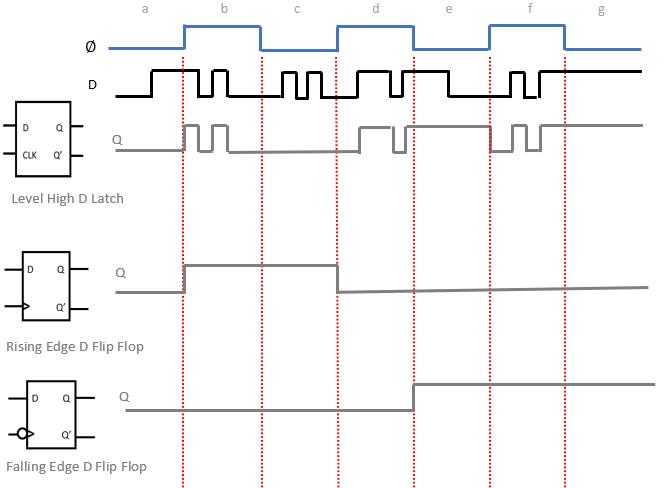
144
Fig. 6‐17. Timing diagram examples for a level high D latch, rising edge D flip‐flop, and a falling edge D flip‐flop.
the f to g transition, J = 0, K = 1, which yields Q* = 0 (reset condition). Q = 0 is maintained until the next falling edge transition.
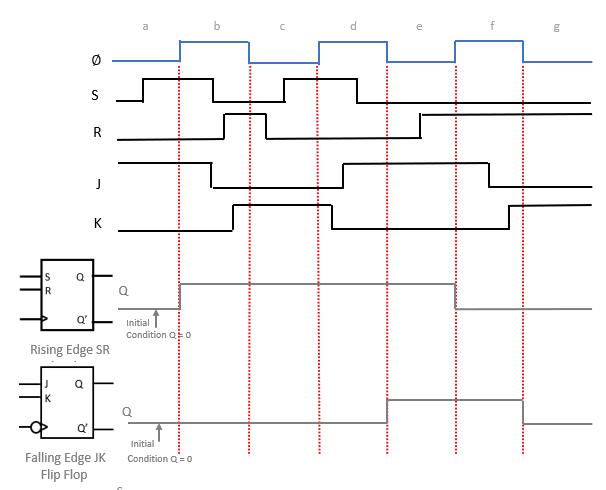
6.6 Flip Flop Applications
Flip flops are commonly used memory elements in the design of digital systems to integrate memory with present binary word inputs to perform and store the result from a variety of arithmetic and logical operations. Registers are the most commonly used storage memory element in digital systems. Registers typically use D FFs with a shared enable/clock. With the shared enable/clock, the inputs and outputs to the D FFs are coordinated to correspond to a single binary word that is being stored (through the inputs at the rising edge of the enable/clock) and read (through the outputs of the flip flops that are held constant between rising edge portions of the enable/clock signal). An example of an 8-bit register is shown in Fig. 6-19 below.
145
Fig. 6‐18. Timing diagrams for a rising edge SR flip‐flop and a falling edge JK flip‐flop.
A shorthand notation for a grouped 8-bit word is given below. From Chapter 5, this 8-bit word is accessed as a single, shared unit or medium, referred to as a bus.
A second flip flop application is a shift register. Shift registers are used for serial communication, bit operations, and arithmetic operations. The following shift register in Fig. 6-20 has eight DFFs sharing a common enable/clock signal with a single external bit input to the first DFF in the sequence, the output of the DFF is given as an input to the next DFF, repeating the sequence with the shift register output as the output of the last DFF. At each rising edge of the enable/clock signal, the input D is received into the shift register. Each bit is shifted one position to the right, with the eighth bit shifted to the output Q. This configuration is a first-in, first-out shift register.
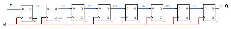
Another configuration given in Fig. 6-21 below receives all bits into the shift register concurrently through a common enable/clock signal to all registers in the shift register. There are four operations that can be performed on the shift register values, including SHR (shift right), SHL (shift left), ROR (rotate right), and ROL (rotate left). All bits of the shift register can be accessed (read as outputs) concurrently. This configuration is referred to as a parallel input/parallel output shift register.
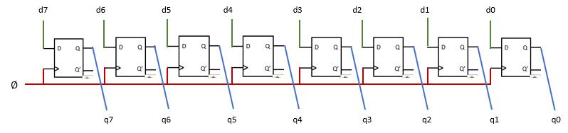
146
Fig. 6‐19. 8‐bit register using D flip‐flops.
Fig. 6‐20. First‐in, first‐out shift register.
The four operations of the shift register from Fig. 6-21 are illustrated as follows:
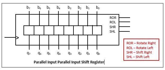
Let N = 01110100 be the input to the shift register. Each operation is performed separately on N.
SHR 2 (shift right 2 positions). This operation shifts the bits of N two positions to the right. The first shift right is as follows: 01110100. The bit in orange is shifted out, all of the remaining bits are moved one position to the right, and a 0 is shifted in as the most significant bit. The second shift right is: 00111010. Again, the bit in orange is shifted out, the bit in yellow is shifted in, with all of the bits moved one position to the right. The final word in the shift register after this operation is: 00011101.
SHL 3 (shift left 3 positions). This operation shifts the bits of N three positions to the left. The first shift left is as follows: 01110100. The bit in orange is shifted out, all of the remaining bits are moved one position to the left, and a 0 is shifted in as the least significant bit. The second shift left is: 11101000. Again, the bit in orange is shifted out, all of the remaining bits are moved one position to the left, and a 0 is shifted in as the least significant bit. The third shift left is: 11010000. Again, the bit in orange is shifted out, all of the remaining bits are moved one position to the left, and a 0 is shifted in as the least significant bit. The final word in the shift register after this operation is: 10100000.
ROR 4 (rotate right 4 positions). This operation rotates the bits of N four positions to the right, taking the bit out of the least significant bit position and moving it to the most significant bit position The ROR operation after each bit rotation:
1 bit: 00111010
2 bits: 00011101
3 bits: 10001110
4 bits: 01000111
Final result: 01000111
147
Fig. 6‐21. Example of a parallel input parallel out shift register.
ROL 5 (rotate left 5 positions). This operation rotates the bits of N four positions to the left, taking the bit out of the most significant bit position and moving it to the least significant bit position. The ROL operation after each bit rotation:
1 bit: 11101000
2 bits: 11010001
3 bits: 10100011
4 bits: 01000111
5 bits: 10001110
Final result: 10001110
Note that the rotate operations retain all of the data bits in N. The bits are moved (rotated) to different positions in the word. The shift operation loses values of the data bits that are shifted out and the 0s replaced in the voided shift bit positions.
6.7 Random Access Memory
Random access memory (RAM) is a general-purpose memory, often configured in large arrays, is used to store data in digital systems such as computers. There are several types of RAM cells. Two types overviewed here include static random access memory (SRAM) and dynamic random access memory (DRAM) cells.
In SRAM cells, illustrated in Fig. 6-22, two inverters are cross-coupled with the output of one inverter fed as the input to the second inverter, and the output of the second inverter is fed as the input to the first inverter. This configuration allow the data value and its complement to be maintained (stored) and accessed (read). Each inverter uses two CMOS transistors (1 pFET and 1 nFET) for a four transistor implementation for each memory cell. These memory cells are configured use an enable (E) or word line connected with switches to enable storing and reading a data bit (D) and its complement (D’) in the memory cell when E = 1 or holding a data bit (D) and its complement (D’) with E = 0 in the memory cell.
A second memory cell configuration is based on dynamic RAM (DRAM). In a DRAM cell, the bit value D passes through an nFET with the nFET’s gate terminal connected to a wordline (WL). The passed through value D goes through a capacitor, which is charged to store the data value D. The schematic for the DRAM cell is shown in Fig. 6-23 below. The charged capacitor voltage (Vs) contains the bit value D. When WL = 1, D can be written or read from the memory cell. When WL = 0, the data value is held in the capacitor. After the capacitor is charged and WL = 0 to hold the data value, there is leakage current (Is) to discharge the capacitor over time. Thus, DRAM cells require refreshing the data values stored to retain those values. SRAM memory cells do not require refreshing because the inverter configuration does not leak current in holding the data value.
148
An example of an SRAM memory array component is given in Fig. 6-24 below. This component uses eight SRAM memory cells with a common word line provided as the output from a 3 to 8 decoder. This component contains eight unique 8 bit words. The control word for the decoder (210) contains address lines A2 A1 A0, where the combination of A2 A1 A0 refers to the memory location of the 8 bit data word stored in the SRAM memory array. The SRAM memory array component contains data input, data output, an Enable, and a Read/Write selector to allow the memory component to read/write data in 8 bit words to a designated memory location A2 A1 A0 by enabling the device and selecting Read/Write. In read mode, the 8 bit word at the designated location A2 A1 A0 is given to the data output. If the memory component is not enabled, all of the 8 bit values are held and cannot be accessed.
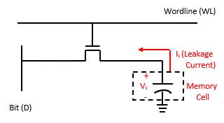
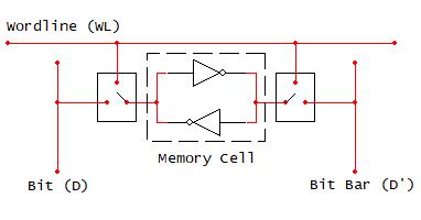
149 SRAM Cell
Fig. 6‐22. SRAM cell and bit configuration illustrations.
Fig. 6‐23. DRAM cell and bit configuration illustration.
An example of an SRAM component symbol for storing 64 words of 8 bit values is shown in Fig. 6-25 below. The component shown on the left highlights the 64 rows of 8 bits stored in the memory array with the read/write (R/W) and enable (Enable) signals and the address lines (A5 A4 A3 A2 A1 A0) for each 8 bit word stored, represented as d7 d6 d5 d4 d3 d2 d1 d0. The component shown on the right is the symbol for an SRAM memory array. The line with a 6 for the address corresponds to the address lines (A5 A4 A3 A2 A1 A0) to access each word stored in the memory array and the data line with an 8 to represent an 8 bit word (d7 d6 d5 d4 d3 d2 d1 d0) associated with each address.
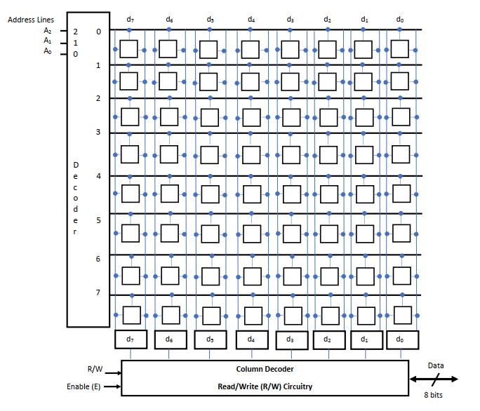
150 8x8 SRAM Device
Fig. 6‐24. 8x8 SRAM device.
A memory array example problem is presented below to illustrate how memory array components can be used as building blocks to generate larger memory array configurations. Larger memory configurations may be larger word sizes (data) for a given number of words (addresses), larger numbers of words (addresses) for a given word size (data), or combinations of larger word sizes (data) with a larger number of words (addresses). The example below shows a memory array configuration with 32 word x 8 bit word size component as a building block to obtain a larger number of words that can be stored and accessed with an 8 bit word size. In this example, there are 4 32 x 8b SRAM components that share R/W pins and are tied to a common 8 bit word (data) for reading and writing to the overall memory array component. Each 32 x 8 bit SRAM component has a different enable condition based on the combinations of the address lines A6 A5. Each 32 x 8 bit SRAM component shares the common 32 addresses given by A4 A3 A2 A1 A0 with 8 bit word sizes. Combinations of A4 A3 A2 A1 A0 access the same address (memory location) on each of the four components. However, the enable combination of A6 A5 determines which component is accessed with the designated A4 A3 A2 A1 A0 address. The two questions asked for this example are the: 1) word size associated with the memory array configuration and 2) range of addresses associated with each of the four SRAM memory components. For question 1, the outputs of all four SRAM components are tied together to access an 8 bit (b7 b6 b5 b4 b3 b2 b1 b0) data value. Based on the enable condition specified by A6 A5, only one of the four SRAM components accesses (read/write) the shared 8 bit data pins. Pins are stated here as a reminder that the SRAM components are integrated circuits with pins for the addresses, read/write, enable, and data values (inputs for write and outputs for read). So, the word size for this memory array is 8 bits. For question 2, the address space for each of the four SRAM components refers to the range of addresses (memory locations) that are accessed by each component. The total number of unique addresses among the four SRAM components determined the total number of words that can be accessed in the SRAM configuration. An address table is used to determine the number of words and the addresses of those words for each SRAM component. The address table contains separate columns for each address line tied to the individual SRAM components and to the enables for the individual SRAM components. In this example, there are seven address lines (A6 A5 A4 A3 A2 A1 A0). Address lines A4 A3 A2 A1 A0 are common to each of the SRAM components, so share the 32 addresses from 0 0 0 0 0 (0) (start) to 1 1 1 1 1 (31) (end). The top SRAM component (labeled as 1) in the address table is enabled by A6 A5 = 0 0. The second SRAM component from the top (labeled as 2) in the address table is enabled by A6 A5 = 0 1, with A4 A3 A2 A1 A0 having the same possible combinations as for component 1 (or any of the four components). The address
151 Address Lines (A5…A0) Data Lines (d7…d0) 6 8 R/W E
Fig. 6‐25. 64x8 SRAM device symbol.
64 x 8b SRAM
table lists the start and end addresses for each of the four SRAM components, which is shown in the solution below. In order to determine the number of unique words accessible in the memory array, the combinations of A6 A5 A4 A3 A2 A1 A0 are examined for accessing the 32 words for each SRAM component. Overlaps in the A6 A5 A4 A3 A2 A1 A0 combinations among the four SRAM components refer to shared addresses between those SRAM components, which results in the words accessed by those SRAM components being combined as the data pins. For this example, the A6 A5 A4 A3 A2 A1 A0 combinations are unique for each of the four SRAM components, so there are 128 unique words accessible in the memory array. Since the words are uniquely addressed on each SRAM component, the accessed words are 8 bits to maintain the word size for each SRAM component.
Example Problem:
Given the block diagram for the memory array below, answer the following questions.
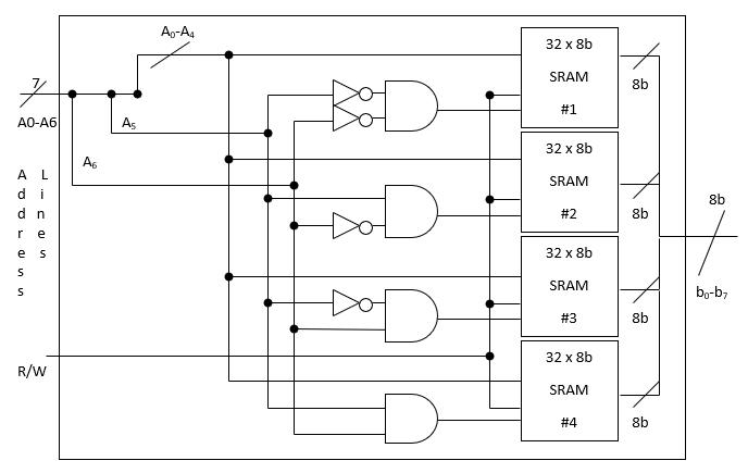
a) What is the size of the memory array?(How many different words are stored in the memory array? What is the word size constructed from the four 32x8b SRAM devices?)
Different words: 32 words per SRAM device x 4 devices with unique addresses = 128 unique words
Word size: Each SRAM device has 8 bit data words. Since the addresses for all four devices are unique, each address has an 8 bit data word.
Size of the memory array: 128 words x 8 bits
152
b) What is the address space for each of the four 32x8b SRAM devices? (What are the starting and ending addresses for each of the 32x8b SRAM devices?)
6.8 Arithmetic and Logic Operation Temporary Storage
Another application for flip flops is the storage of intermediate values for arithmetic and logical operations in digital systems such as ring counters and arithmetic logic units. A ring counter uses the inputs to multiplexers to provide data values for operations corresponding to the control word selected. Multiplexers can be used in parallel with a shared control word to allow associated multiplexer inputs to provide multi-bit words for the operations to be performed for the designated control word. The results of the operations are stored in latches or flip flops for each data bit. An example of a ring counter is shown in Fig. 6-26 below. The table presents the operations performed based on the control word combinations for S1 S0. This ring counter uses 4 bit data values for each operation. For the 4 bit word A = a3 a2 a1 a0, the inputs for the multiplexers are shown to perform the control word designated operation, with the leftmost and rightmost multiplexers and latches corresponding to the most and least significant bit positions, respectively. For S1 S0 = 0 0, the operation is to clear all bits. Each input 0 for the four multiplexers is labeled 0, so that all bits are cleared. For S1 S0 = 0 1, the operation is to toggle all bits. The current complements of the outputs of the four latches (Q3’ Q2’ Q1’ Q0’) are fed into the corresponding multiplexer 1 inputs. These toggled values update the outputs of the corresponding latches. For S1 S0 = 1 0, the operation is shift right with wrap around. This is equivalent to ROR 1. The current output Q0 is wired to multiplexer 2 input for Q3. The current output Q1 is wired to multiplexer 2 input for Q0. The current output Q2 is wired to multiplexer 2 input for Q1. The current output Q3 is wired to multiplexer 2 input for Q2. For S1 S0 = 1 1, the operation is shift left, with no wrap around. This is equivalent to SHL 1. The current output Q2 is wired to the multiplexer 3 input for Q3. The current output Q1 is wired to the multiplexer 3 input for Q2. The current output Q0 is wired to the multiplexer 3 input for Q1. The multiplexer 3 input for Q0 is wired ground (0 shifted into the least significant bit).
153
Start Address End Address Device A6 A5 A4 A3 A2 A1 A0 A6 A5 A4 A3 A2 A1 A0 1 0 0 0 0 0 0 0 0 0 1 1 1 1 1 2 0 1 0 0 0 0 0 0 1 1 1 1 1 1 3 1 0 0 0 0 0 0 1 0 1 1 1 1 1 4 1 1 0 0 0 0 0 1 1 1 1 1 1 1
Function Table
In a typical user interactive computer’s organization, there are three core components, including a central processing unit (CPU), a datapath, and memory, as illustrated below. The CPU uses the address bus in the datapath to access memory for code and data for accessing and executing instructions. Memory includes code and data memory for storing program instructions and accessing and storing data. The datapath also provides address and data buses for user interaction peripheral devices such as a mouse, keyboard, monitor, and printer. The CPU includes several components, including a control unit for coordinating the fetch, decode, and execution of program instructions and an arithmetic logic unit (ALU) to perform arithmetic and logical operations that
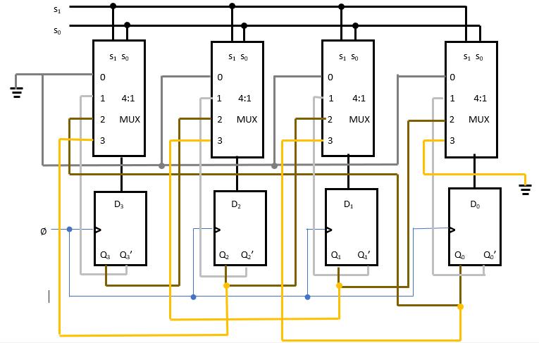
154 Ring Counter Example
Fig. 6‐26. Ring counter example.
S1S0 Action (In words) 00 CLEAR ALL BITS 01 TOGGLE ALL BITS 10 SHIFT RIGHT with wrap around 11 SHIFT LEFT with no wrap around
are associated with the computer program instruction set. Below is an illustrative figure of computer organization (Fig. 6-27) and an example of a 4-bit ALU (TTL 74181) (Fig. 6-28).
Address Bus CPU
Memory Peripherals ALU
Control Unit Program (ROM) Devices such as Registers Data (RAM) a keyboard, printer Cache Clock Data Bus
This ALU has a 5 bit control word S3 S2 S1 S0 M to select an arithmetic or logical operation. There are two 4 bit words input (A and B) with the control word to provide data for the different operations and a 4 bit output word F. There is an initial carry input (Cin) and a carry out (Cn+4) output for arithmetic operations. Cin is active low, so Cin = 0 is interpreted as an initial carry of 1 and vice versa. The ALU utilizes multiplexers to coordinate data flow for the different operations in a similar manner to the ring counter.
155
Fig. 6‐27. Microprocessor computer organization illustration.
4 bit ALU (TTL 74181)
Control word: S3 S2 S1 S0 M
Inputs: A = A3 A2 A1 A0, B = B3 B2 B1 B0, Cn (active low)
Outputs: F = F3 F2 F1 F0, Cn+4
Output flag: A=B
G, P: For cascading carry output with additional adder ICs
Fig. 6‐28. 4‐bit ALU (TTL 74181) with arithmetic and logical operations1
As an illustration of the logic gate and digital component implementation described in previous chapters, the logic diagram for this 4-bit ALU is presented in Fig. 6-29.
156 A0 M B0 S3 A1 S2 B1 S1 A2 S0 B2 A3 B3 G P Cn F0 A=B F1 F2 F3 Cn+4 election Logic Operation Arithmetic Operation s3 s2 s1 s0 Logic (M = 1) Arithmetic (M = 0, Cin = 0 for active low input) 0 0 0 0 F = A’ F = A 0 0 0 1 F = (A+B)’ F = A+B 0 0 1 0 F = A’B F = A+B’ 0 0 1 1 F = 0 F = Minus 1 0 1 0 0 F = (AB)’ F = A+AB’ 0 1 0 1 F = B’ F = (A+B) Plus AB’ Plus 1 0 1 1 0 F = AꚚB F = A minus B 0 1 1 1 F = AB’ F = AB’ 1 0 0 0 F = A’ꚚB F = A Plus AB Plus 1 1 0 0 1 F = (AꚚB)’ F = A Plus B Plus 1 1 0 1 0 F = B F = (A+B’) Plus AB Plus 1 1 0 1 1 AB AB 1 1 0 0 1 A Plus A Plus 1 1 1 0 1 A+B’ (A+B) Plus A Plus 1 1 1 1 0 A+B (A+B’) Plus A Plus 1 1 1 1 1 A A
Reference
1 http://pdf.datasheetcatalog.com/datasheets/700/493319_DS.pdf. Texas Instruments component. Last accessed Jan. 24, 2022.
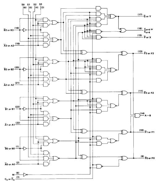
157
Fig. 6‐29. Logic gate implementation of 4‐bit ALU1
Chapter 7: State Machines
Chapter 7 Learning Goals
Logically interpret state machine circuits
Design basic digital counters and other finite state machines
Chapter 7 Learning Objectives
Understand the concept and terminology for state machines
Define Finite State Machines (FSM) and basic components used in FSM design and implementation
Define and apply a state table for state machine circuit design and interpretation
Define and apply a state transition diagram for state machine circuit design and interpretation
Apply and interpret flip-flops as memory elements in state machine circuit design and interpretation
Design counters and other state machine circuit applications
Understand Mealy and Moore state machines
Define and apply the state machine digital circuit design process
158
7.1 Overview of Finite State Machines
This chapter introduces circuit design that integrates combinational logic circuits with memory. Finite state machines, also known as sequential circuits or sequential networks, are digital systems where the output is determined by present inputs and the result of earlier events (memory). In synchronizing the circuit operation with memory and present inputs, a periodic clock signal is used. Fig. 7-1 shows the basic components used in state machine circuits. Synchronous sequential networks utilize this synchronizing clock signal to control the flow of data.
Let’s consider a counter as a synchronous sequential counter. In the schematic in Fig. 7-2 (below), a clock signal is used to provide rising edge pulse inputs to increment (add 1) to a 3 bit number, which is output as the binary word q2 q1 q0. A secondary output (R) is generated which logically ANDs q2 q1 q0. The count sequence for q2 q1 q0 goes through 000 => 001=>010=>011=>100=>101=>110=>111=>000… or 0=>1=>2=>3=>4=>5=>6=>7=0…
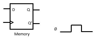
From this count sequence, R = 0 for counts q2 q1 q0 000=>001=>010=>011=>100=>101=>110 and becomes R = 1 when q2 q1 q0 = 111. So, R = 1 when the count sequence is at its maximum count and will reset (000 with R = 0) on the next clock pulse. Accordingly, R is referred to a flag. The count sequence can also be represented using nodes for the transitions between counts with the output flag, R, given for each output. Each node, representing a count in the sequence is referred to as a state with an associated input/output for each state. In this counter, there is no external input variable, and there is one output variable generated (R). This nodal sequence with each count and associated external input (no input in for the counter)/output (R) at each count is referred to a state transition diagram. In the notation used, the inputs/outputs are present values associated with each state. External inputs are given to the left of /, and outputs are given to the right of /. The clock pulse input does not represent an external input variable. Rather, the clock pulses provide a synchronizing signal that causes the synchronous sequential circuit to change states with each clock pulse. Each state has an associated present output R, which represents whether the count is about to reset. A state is a stable condition, meaning that a state cannot change until a clock pulse (synchronizing pulse) with or without an external variable input is provided to cause a change in state. Each of the three bits that form the count within each node are binary
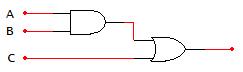
159
Combinational Logic Clock (Synchronizer)
Fig. 7‐1. Components used in state machine circuits such as a counter.
variables that change based on the state transitions (changes in the count). These binary variables maintain their values between clock pulses or between changes in externally applied input variables (again, there are externally applied variables for the counter example below). Since the binary variables maintain their values until an event (clock transition in this case, or a change in an externally applied input variable) leads to a change in the binary variables, these binary variables are represented as the outputs of memory elements which are conventionally DFFs. The outputs of the memory elements representing the binary variables in sequential circuits are referred to as state variables. For this counter example, there are three state variables, which when put in the form of a binary word define the states of the sequential circuit.
160
Pulses 0‐7 Counter Input Increment Number Reset Flag R Current count q2 q1 q0 State Transition Diagram q2 q1 q0 inputs/outputs No external inputs /1 0 0 0 /0 Output: R 1 1 1 0 0 1 State node 1 1 0 0 1 0 State transition 1 0 1 0 1 1 1 0 0 State variables (Flip flop outputs) q2 q1 q0
7
/0 /0 /0 /0 /0 /0
Fig.
‐
2. 3‐bit counter circuit with state transition diagram (extended from1).
7.2 Sequential Circuits with 1 or 2 State Variables
In this section, sequential circuit examples are given with one or two state variables. These examples build off of sequential circuit examples presented in Uyemura1. The process to determine the behavior of these circuits is presented, including the determination of the state transition diagram. In sequential circuits, a state variable is represented as the output Q of a flip flop. The number of flip flops in a sequential circuit represents the number of state variables, as given by the outputs of the flip flops.
The following example presents the process to analyze sequential circuits to find the state transition diagram. This example has a single state variable, the output (X) of the DFF, a single externally applied input variable C, and one output T. The input to the DFF is denoted as DX, with the flip flop type and the associated flip flop output X as the subscript. Looking at this circuit, the direction of data flow is important to understand to represent the logical flow. The arrows shown on the circuit show the data flow, which is needed to find the inputs and outputs of each logic component and flip flop to determine the internal logic expressions. The data flow comes from the output of a flip flop with data flow going into the flip flop input. In the example circuit below, the DFF output X provides an input to the exclusive or gate with input C. The exclusive or gate output provides the output (T) for the circuit and the input (DX) to the DFF. Sequential circuits have a clock signal that is used to synchronize operation of the circuit with the externally applied inputs and the state variables from the memory elements (flip flops) that are fixed between the rising edge periods of the clock signal to determine the outputs of the circuit and the updated state variable values stored in memory elements.
In the example circuit in Fig. 7-3 below, the process is presented for analyzing the circuit is given to derive the behavior of the circuit using a state table and a state transition diagram. The state table is a truth table for the sequential circuit that includes the circuit inputs and outputs (combinational logic inputs), the present state variable values (flip flop outputs before the rising edge clock transition), the flip flop inputs that are used to determine the next state variable values (flip flop outputs after the rising edge clock transitions), and the next state variable values. For notational purposes, X refers to the present state (output of the flip flop before the rising edge transition) and X* refers to the next state (output of the flip flop after the rising edge transition which utilizes the externally applied input C to the DFF input DX). Recall that the flip flop output for a rising edge flip flop uses the flip flop’s input value(s) at the rising edge transition, applies the flip flop’s truth table to determine the flip flop output after the rising edge transition. The state transition diagram uses the form from the previously presented 3-bit counter example. The state transition diagram presents a visual representation of the individual states (state variable combinations) with the associated circuit output values while the circuit is in those states, and externally applied input values while the circuit is in different individual states to show the circuit transitions to its next state (new state variable combinations based on the starting or present state variable combinations).
161
The process to determine the state transition diagram from the sequential circuit is given with the following steps:
1) Write all logic relationships from the circuit.
�� �� ��∗ where * denotes after the clock transition
Clock transition flip flop value change (rising edge DFF used in this circuit):
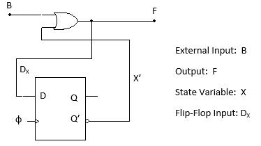
X X* X: Present state (output of DFF) before the clock transition X*: Next state (output of DFF) after the clock transition
2) Determine the state table.
The state table is a listing of the present values of the input(s), state(s), output(s), flip flop, and the input(s), as well as a listing of the next state(s) (after the clock transition).
162
Fig. 7‐3. Single state variable circuit example. NEW EXAMPLE.
�� �� ��′
�� �� ��′ �� �� ��∗ State Table Present input Present state Present output Next state Flip flop input B X F X* DX 0 0 1 1 1 0 1 0 0 0 1 0 1 1 1 1 1 1 1 1 DFF Truth Table D Q* 0 0 1 1
The state table from step 2 is applied to determine the state transition diagram (also known as the state diagram) in step 3. With one state variable (X), there are two nodes in the state transition diagram (X=0 and X = 1). For each row (entry) in the state table, the arc connections are made between the nodes in the state table, labeling the input/output combinations associated with output associated with the state and the input that causes the transition to the next state. The arc connections for the state transitions include arrows to indicate the direction of state transition. In the first state table row entry, the present state X = 0 has an associated output F = 1 (/1 on the arc to designate the present output for this state) and an input B = 0 which yields a state transition to X* = 1, where X* refers to the next state. In the state transition diagram below, an arc is drawn with an arrow from the node X = 0 to the node X = 1, labeling the input B=0/F=1. The second state table entry has a present state X = 1 and next state X* = 0. So, an arc with an arrow is drawn from the node X = 1 to X= 0 with B=0/F=0 on the arc to indicate the output for this state (F=0) and the input B=0 which causes this state transition. The third state table entry has a present state X = 0 and next state X* = 1. The arc from the node X = 0 to X = 1 is reused since the first entry in the state table also has the state transition from X = 0 to X = 1, putting a comma with B=1/F=1. The final state table entry has X = 1 and next state X* = 1. An arc with an arrow is drawn from the node X=1 to X=1 with B=1/F=1. The state transition diagram is shown below.
3) Draw the state transition diagram (or state diagram).
From this example, note that the state transition diagram: 1) has 21 = 2 nodes (states), where 1 is the number of state variables (flip flops) in the circuit and 2) does not include any details about the flip flop type used to represent the state variables.
A second single state variable sequential circuit is shown in Fig. 7-4 below. From the circuit, the analysis process is applied to find the state transition diagram. In this circuit, there are two externally applied input variables (c, d), one output (f), and one state variable (X).
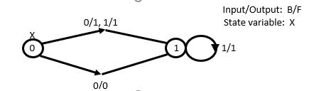
163
Analysis steps:
1) Write all logic relationships from the circuit.
2 input variables: c, d
Output: f State variable: X
2) Determine the state table using the equations from step 1.
The number of rows in the state table is given based on the number of input and state variables. In this example, there are two inputs (c, d) and one state variable (X), giving 2(2+1) = 23 = 8 entries.
164
Fig. 7‐4. Another single state variable sequential circuit analysis example to find the state transition diagram.
�� ���� �� = (c’+X’)d �� �� �� ∗
�� ��′ ��′ �� �� ��′ ��∗ Present Input Present State Present Output Next State Flip Flop Input c d X f X* DX 0 0 0 0 1 1 0 0 1 0 1 1 0 1 0 1 0 0 0 1 1 1 0 0 1 0 0 0 1 1 1 0 1 0 1 1 1 1 0 1 0 0 1 1 1 0 1 1 c d f ф D Q Q’ DX X
3) Draw the state transition diagram.
Inputs/output:
In this example, there are two states providing the possible values of the state variable X. There are two externally applied input variables (c d) and one output variable (f). For each state variable value (X = 0 or X = 1), each combination of input variables (c d) provides a change to the state variable (next state referred to as X*). The input combinations are given to the left of the / with the directed arc going to the next state. The output (f) shown to the right of the / is the present output of the circuit when the circuit is in the current state. Fig. 7-5 shows the resulting state transition diagram.
In example 3 below, the sequential circuit shown in Fig. 7-6 has two state variables (X and Y), one externally applied input (S), and two outputs (F and G). Similar to the previous two examples, the circuit is analyzed to find the state table and state transition diagram.
165
cd/f 00/0, 10/0 State variable: X 01/1, X 10/0, 0 1 00/0, 11/0 11/1 01/1
Fig. 7‐5. State transition diagram for circuit shown in Fig. 7‐4.
Find the state transition diagram from the sequential circuit.
DX DY X Y F G S DX D Q Q Q’ Q’ ф
S Outputs: F, G State variables: X, Y D X’
Fig. 7‐6. Sequential circuit example with two state variables.
Input:
The same steps are applied to analyze the circuit. Given the inputs, state variables, and outputs, the logic relationships are determined to characterize the operation of the circuit (as given in step 1 below). After finding the logic relationships, the state table is determined. The externally applied input (S) (also referred to as the present input), and the present values of the state variables (X and Y values before the shared rising edge clock transition for the DFFs) provide all of the combinations that the sequential circuit can transition based on the logic relationships and the flip flop input truth table translation to the flip flop outputs after the clock transition. S, X, and Y provide the possible combinations of the circuit operation such that the truth table has 23 = 8 entries. For each combination of S, X, and Y, the outputs F and G, and the flip flop inputs DX and DY are determined. The next state X* and Y* values are found based on the present state values and the flip flop inputs DX and DY, respectively, with the flip flop truth tables. For the DFFs in this sequential circuit, the DFF truth table is represented as DX = X* and DY = Y*, respectively. The state table is shown below in step 2. Using the state table, the state transition diagram is obtained. With two state variables (two flip flops), there are 22 = 4 possible states or combinations of the state variables X and Y. X and Y can be 00, 01, 10, and 11. Thus, there are four nodes in the state transition diagram. For each entry in the state table, an arc with an arrow in the direction of the present state to next state transition is drawn. With the arc, the input/output combinations are labeled. In this example, the input/output combinations are S/F G (one input and two outputs). The interpretation of the directed arc with the input/output combinations corresponding to the state table entry is the present state for X Y with the input S results in the state transition to the next state X* Y*. The outputs ax ay are the outputs of the sequential circuit while in this present state X Y. The state transition diagram for step 3 is shown in Fig. 7-7 below.
Steps to find state transition diagram:
1) Logic relationships from the circuit.
2) Find the state table.
166
�� �� ��′ �� ��⨁��⨁�� �� �� �� ∗ �� �� ��∗
�� �� ��′ �� ��⨁��⨁�� �� �� ��∗ �� �� ��∗ Present Input Present State Present Output Next State Flip Flop Input S X Y F G X* Y* DX DY 0 0 0 1 0 1 0 1 0 0 0 1 1 1 1 1 1 1 0 1 0 0 1 0 1 0 1 0 1 1 0 0 0 0 0 0 1 0 0 1 1 1 1 1 1 1 0 1 1 0 1 0 1 0 1 1 0 1 0 1 0 1 0 1 1 1 1 1 1 1 1 1
There are a number of notations for labeling the states and the input output combinations associated with and the transition in states. A second notation for labeling states with inputs and outputs is given below for the state S1. Each state has a label that corresponds to a combination of the state variables. S1 = 01 (for present values of the state variables X=0, Y=1). While in state S1, the outputs of the circuit are F and G. The input S is labeled as providing the transition from S1 to S2.
7.3 Mealy and Moore Machines
There are two types of state machines: Mealy and Moore. A Mealy machine is a sequential circuit where the output of the circuit is a function of the present state (state variables) and present input. Examples 1-3 above are examples of Mealy machines. A Moore machine is a sequential circuit where the output is a function of the present state (state variables) only. The 0-7 counter presented in the opening of this chapter is an example of a Moore machine.
167
0/0 1 Input/outputs: S/FG 0 1 State Variables: X Y 1/10 0/10 0/01 0 0 10 1/10 X Y 1/11 0/01 0/00 1 1 1/11
3) Find the state transition diagram.
Fig. 7‐7. State transition diagram for sequential circuit from Fig. 7‐5.
S1 F G S S1 = 0 1 = X Y S0 S2 S3
7.4 Sequential Circuit Design
In the previous section, sequential circuits were analyzed to describe their behavior based on the state table and the state transition diagram. In this section, the design and implementation of sequential circuits are explored using state transition diagrams and state tables to characterize the behavior of the circuits. In the previous section, the output of a memory element (flip flop) (output value after the clock transition) is determined based on the memory element input. For a DFF, the truth table is:
For sequential circuit design, the opposite problem is examined. Namely, the input of the flip flop needs to be determined to produce a specific flip flop output. In order to accomplish this, the excitation table for a flip flop is found. The excitation table specifies every state transition combination with the associated flip flop inputs to produce that state transition. The excitation table for a DFF is given in Fig. 7-8 below.
1
0 Corresponds to current output Q = 0. With current input D = 1, the flip flop output after the rising edge transition (denoted as Q*) is Q* = D = 1. Q* becomes the current output Q until the next rising
For a DFF, the input D equals the next state Q*. So, there is no relationship between the present output Q and the flip flop input D with the next state Q*.
The excitation table for a JK FF is given in Fig. 7-9 below. The JK FF table is provided as a reference. For the first entry, to get from the present output of the JK FF Q = 0 to the next state Q* = 0 requires JK FF input values of J and K? From the JK FF truth table, in order to obtain Q* = 0, either J = 0, K = 1 to reset the flip flop output Q* = 0 OR J = 0, K = 0 to keep the present flip flop output Q = 0 after the clock transition to be Q* = 0. For both cases, J = 0. K can be 0 or 1 for the Q = 0 to Q* = 0 to occur, which means that J = 0 and K is a Don’t Care (X). For the second entry in the Excitation Table, to get from the present output of the JK FF Q = 0 to the next state Q* = 1 requires either J = 1, K = 0 to set Q* = 1 OR J = 1, K = 1 to toggle Q = 0 to Q* = 1. Thus, J = 1, K = X for the state transition Q = 0 to Q* = 1. The remaining entries in the Excitation table are found in a similar manner.
168
D Q* 0 0 1 1
To go from Q To the next state Q* Needs an input of D 0 0 0 0 1 1 1 0 0 1 1 1
Fig. 7‐8. Excitation table for a DFF.
Excitation Table for a JK FF
7.4.1 Sequential Circuit Design Process
X denotes a Don’t Care condition
The sequential circuit design process is illustrated through the following example based on a given state transition diagram (shown in Fig. 7-10) and flip flop memory element for the state variable. A DFF is to be used for the state variable.
Inputs/output: S/F
State variable: X
169 To go from Q To the next state Q* Needs inputs of J K 0 0 0 0 0 0 X 1 0 1 1 1 1 0 X 1 1 0 0 X 1 1 1 1 1 1 0 X 1 0 0 0
Fig. 7‐9. Excitation table for a JK FF.
0/1
X 1/0 0 1 0/0 1/1
J K Q* 0 0 Hold (Q) 0 1 0 1 0 1 1 1 Toggle (Q’)
Fig. 7‐10. State transition diagram for state machine design.
For the state transition diagram in Fig. 7-10, there is one state variable (one flip flop), one externally applied input, and one output. The first step in the design process is to find the Excitation table for the flip flop used for the state variable. For step 1, the Excitation table for the DFF is presented. The second step in the design process is to identify and label the state variable (X), input (S) and output (F). The third step is to find the state table based on the state transition diagram and the DFF Excitation table. There is one state variable (A) and one present input (X) which gives the next state (X*), output (F), and DFF input (DX) in the state table. Given the present value combinations of S and X, there are four entries (2(# inputs + # state variables)) 22 = 4. For the entry X = 0 and S = 0, F = 1 while in this state, and the state transition diagram shows a transition to X* = 1. Using the Excitation table entry to get from X = 0 to the next state X* = 1 requires an input of DX = 1 (DX = X* for the DFF). For the second entry, X = 0 and S = 1, F = 0 while in this state, and the state transition is to X* = 0. For the third entry, X = 1 and S = 0, F = 0 while in this state, and the state transition is to X* = 1 requiring DX = 1 (based on the Excitation table entry X = 1 to X* = 1 requires DX = 1. For the final entry, X = 1 and S = 1, F = 1 while in this state, and the state transition is to X* = 0 requiring DX = 0.
Upon completing the state table, step 4 is to find minimal Boolean expressions for the circuit output (F) and the flip flop input (DX) in terms of the present input (X) and state variable (S). The column for F is a function of S and X in forming the 2-variable K-map. From the K-map for F, F = S’ + X. Similarly, the minimal expression for DX is found using the 2-variable K-map for the variables S and X, which is determined as �� ��⨁�� . Step 5 is to find and implement the sequential circuit that behaves according to the state transition diagram using the equations found from step 4. To implement the sequential circuit, draw the DFF and label the output (X) (the complemented output X’ can also be labeled), the input (DX), and the clock signal. Then, label the input (S) and output (F) on the circuit in different places on the circuit. Draw the connections for S’ and DFF output X to an OR gate with the output of the OR gate connected to F. Draw the connections between the input and DFF output S to a complemented XOR gate (XNOR) (or the individual terms SX, S’X’ ORed) which is connected to DX. This completes the implementation of the sequential circuit.
The process for state machine design includes the following steps:
1) Determine the excitation table for the flip flop used for the memory element. As previously derived and repeated here as a reference, here is the excitation table for a DFF.
2) Determine all variables and state variables.
170
To go from Q To the next state Q* Needs an input of D 0 0 0 0 1 1 1 0 0 1 1 1
From the state transition diagram, there are one input variable, one output variable, and one state variable, designated as:
Input variable: S Output variable: F State variable: X
3) Determine the state table from the state transition diagram. Use the excitation table from step 1 to find the flip flop input DX for the state variable X.
4) Determine the minimal Boolean expressions for the state element input(s) (flip flop input(s)) and the output(s).
5) Construct the sequential circuit that behaves according to the state table using the DFF for the state variable, input(s), output(s), and the minimal Boolean expressions for the DFF input and the output
171
State Table Present input Present state Present output Next state Flip flop input S X F X* DX 0 0 1 1 1 0 1 0 1 1 1 0 0 0 0 1 1 1 0 0
F DX
X S 0 1 0 1 0 �� ���� ���� ���� �� ��⨁�� 1 0 1 X S �� 0 1 0 1 1 �� �� 1 0 0 ф X S DX F D Q Q’
Fig. 7‐11. Sequential circuit implementation for state transition diagram from Fig. 7‐10 using a DFF as the memory element.
7.5 State Machine Examples
In the previous sections, sequential circuit analysis and design processes have been presented. Applications of the analysis and design processes are given in this section.
Sequential Circuit Example
From the sequential circuit shown in Fig. 7-12 below, determine the state table. This circuit has two JK FFs for the state elements, one externally applied input (b) and one output (f).
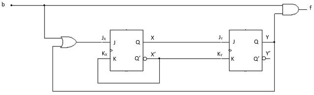
172
Solution Logic equations for circuit behavior: �� �� �� �� ��′ �� �� �� ��′ �� ���� Present Input Present State Present Output Next State Flip Flop Input b X Y f X* Y* JX KX JY KY 0 0 0 0 0 0 0 1 0 1 0 0 1 0 1 0 1 1 0 1 0 1 0 0 1 1 0 0 1 0 0 1 1 0 1 1 1 0 1 0 1 0 0 0 1 0 1 1 0 1 1 0 1 1 1 0 1 1 0 1 1 1 0 0 1 1 1 0 1 0 1 1 1 1 1 1 1 0 1 0
Fig. 7‐12. Sequential circuit example for determining the state table (extended from1).
From the sequential circuit analysis process, the expressions to describe the logic flow are determined (shown above). Equations are needed for the output f and the flip flop inputs JX, KX, JY, and KY. The state table is found by labeling the present input (b), present state variables (X, Y), the present output (f), the next state variables (X*, Y*), and the flip flop (state element) inputs (JX KX, JY KY). There are eight rows in the state table (23 (1 input and 2 state variables)). The equations found for f, JX, KX, JY, and KY are used to fill in the entries for those columns. The only columns in the state table that need to be determined are the next states X* and Y*. The truth table for the JK FF is provided below for a reference. The values of X* are found for each row in the state table by using X (present state), JX, and KX and applying the JK FF truth table. From the first row in the state table, X = 0, JX = 0, and KX = 1. From the JK FF truth table, J = 0 and K = 1, Q* = 0 (reset). Thus, X* = 0 (the present state X is not needed to find X* in this case). In the third row of the state table (b = 0, X = 1, Y = 0), JX = 0 and KX = 0. J = 0 and K = 0 is the hold (Q) condition in the JK FF. With X = 1, X* = 1 (hold). This process is applied to the other rows of the state table. Similarly, the present state Y, JY, and KY are known and used to determine Y* for the rows in the state table. The difference between this example and the other sequential circuit analysis problems is that DFFs are used in the other sequential circuit problems so that the next state values can be determined directly from the DFF input values (D = Q*). In this example, JK FFs are used for the state elements. The JK FF truth table entries explicitly force Q* = 0 (JK = 01) or Q* = 1 (JK = 10), and in other entries Q* = Q (JK = 00) and Q* = Q’ (JK = 11), where Q* is a function of Q. Thus, the present value Q is needed to find the next state value Q*.
Binary Counter Design
The next sequential circuit application is the design of a binary counter. This binary counter example continuously cycles through the counts 0,1,2,3,4,5,6,7,0,1,2,3,4,5,6,7,... There are eight counts, 0-7, giving eight unique states. There are no externally applied inputs for this counter other than a clock signal. There are no outputs with the circuit. With eight unique states, three flip flops (DFFs are used here) are needed (23 = 8) as the memory elements for the counter state machine design. Beginning the design process, the state transition diagram is determined (shown below in Fig. 7-13). The state variables (outputs of the DFFs) are denoted as Q2 Q1 Q0. State 111 (7) transitions to state 000 (0) to repeat the binary count sequence.
After determining the state transition diagram, the state table is found. The excitation table for the DFF is given as the relationship D = Q*. With no input or output, the state table consists of the present values for the present state (Q2, Q1, Q0), the next state (Q2*, Q1*, Q0*) (next count after the clock transition), and the DFF inputs (D2, D1, D0). The state table is shown below.
173
Using the state table, the minimal Boolean expressions for the flip flop inputs (normally for the output as well, but there is no output in this counter design) are determined based on the present state combinations. The K-maps for the flip flop inputs are presented as follows.
174 Q2 Q1 Q0 0 0 0 1 1 1 0 0 1 1 1 0 0 1 0 1 0 1 0 1 1 1 0 0
Present state Next state Flip flop inputs Q2 Q1 Q0 Q2* Q1* Q0* D2 D1 D0 0 0 0 0 0 1 0 0 1 0 0 1 0 1 0 0 1 0 0 1 0 0 1 1 0 1 1 0 1 1 1 0 0 1 0 0 1 0 0 1 0 1 1 0 1 1 0 1 1 1 0 1 1 0 1 1 0 1 1 1 1 1 1 1 1 1 0 0 0 0 0 0
Fig. 7‐13. State transition diagram for 0‐7 counter.
D2 D1 Q1Q0 Q2 00 01 11 10 0 0 1 0 1 1 0 1 0 1 Q1Q0 Q2 00 01 11 10 0 0 0 1 0 1 1 1 0 1 0 7 1 6 2 5 3 4 �� �� �� �� �� �� �� �� �� �� �� �� �� �� �� �� �� �� �� �� �� �� �� �� �� ⨁��
The final step in the counter design process is to draw the circuit. The DFFs are drawn with the inputs (D2, D1, D0) and outputs (Q2/Q2*, Q1/Q1*, Q0/Q0*). The expressions are implemented using the DFF outputs as inputs to the logic gates with the outputs of the expressions associated with the DFF inputs. The binary counter circuit is shown in Fig. 7-14. From this circuit, the current count is found as the DFF outputs Q2 Q1 Q0.
Binary Up/Down Counter
An extension of the binary counter is a binary up/down mod counter. Consider the design of a binary up/down mod 6 counter. Also, consider the use of an external input C to control the count. If the input C = 0, then count down. If the input C = 1, then count up. Use DFFs for the state
175 D0 Q1Q0 Q2 00 01 11 10 0 1 0 0 1 1 1 0 0 1
Fig. 7‐14. Sequential circuit for binary counter 0‐7.
�� �� �� Q2 Q1 QQ D2 D1 D0 D D D Q Q Q Q’ Q’ Q’ Q2 Q2’ Q1 Q0 Q1’ Q0’ ф
elements. Use Don’t Cares for the unused states. Fill in the state table and find the next state logic for the most significant bit of the state.
This problem introduces some new terminology. A mod counter refers to the number of counts starting from 0. A mod 6 counter counts through the sequence 0, 1, 2, 3, 4, 5, 0, 1, 2, 3, 4, 5, … For this circuit design, if the external input C = 0 or 1, the count sequence is down and up, respectively. There are six total counts in the sequence. The number of state variables (flip flops) needed is three. Two state variables provide up to 4 counts (22). Three state variables give up to 8 counts (23). Four counts is too few, and eight counts is above what is needed. So, three state variables are used to represent the six counts (000, 001, 010, 011, 100, 101), with two counts unused (6 110, and 7 111). Let Q2 Q1 Q0 denote the outputs of the DFFs for the state variables. Then, D2, D1, and D0 are the corresponding flip flop inputs. There are four present values (C, Q2, Q1, Q0) to determine the number of rows in the state table. There is no output from the circuit other than the counts provided by the state variables (outputs of the flip flops). The next states (Q2*, Q1*, Q0*) and flip flop inputs (D2, D1, D0) also have columns in the state table. For the first entry in the state table, C Q2 Q1 Q0 = 0 0 0 0. With C = 0 and the current count of 0 (Q2 Q1 Q0 = 0 0 0), the next count is a down count from 0 to 5 (Q2 Q1 Q0 = 1 0 1). For the entry C Q2 Q1 Q0 = 0 0 0 1, the current count is 1 (Q2 Q1 Q0 = 0 0 1), with the next count (down count) of 0 (Q2 Q1 Q0 = 0 0 0). For the entry C Q2 Q1 Q0 = 0 1 0 1, the current count is 5 (Q2 Q1 Q0 = 1 0 1), with the next count (down count) of 4 (Q2 Q1 Q0 = 1 0 0). For the entry C Q2 Q1 Q0 = 0 1 1 0, the current count is 6 (Q2 Q1 Q0 = 1 1 0) which is not part of the mod 6 count sequence. So, the next state (down count) is a Don’t Care (Q2 Q1 Q0 = X X). For the entry C Q2 Q1 Q0 = 0 1 1 1, the current count is 7 (Q2 Q1 Q0 = 1 1 1) which is also not part of the mod 6 count sequence. So, the next state (down count) is a Don’t Care (Q2 Q1 Q0 = X X). For the entry C Q2 Q1 Q0 = 1 0 0 0, the current count is 0 (Q2 Q1 Q0 = 0 0 0), with the next count (up count) of 1 (Q2 Q1 Q0 = 0 0 1). For the entry C Q2 Q1 Q0 = 1 1 0 0, the current count is 4 (Q2 Q1 Q0 = 1 0 0), with the next count (up count) of 5 (Q2 Q1 Q0 = 1 0 1). For the entry C Q2 Q1 Q0 = 1 1 0 1, the current count is 5 (Q2 Q1 Q0 = 1 0 1), with the next count (up count) of 0 (Q2 Q1 Q0 = 0 0 0). For the entry C Q2 Q1 Q0 = 1 1 1 0, the current count is 6 (Q2 Q1 Q0 = 1 1 0) which is also not part of the mod 6 count sequence. So, the next state (down count) is a Don’t Care (Q2 Q1 Q0 = X X). For the entry C Q2 Q1 Q0 = 1 1 1 1, the current count is 7 (Q2 Q1 Q0 = 1 1 1) which is also not part of the mod 6 count sequence. So, the next state (down count) is a Don’t Care (Q2 Q1 Q0 = X X). The entries for the flip flop inputs D2, D1, and D0 are determined based on the Excitation table for the DFF (which is given as D = Q*). This completes the state table. The second part of the problem is to find “the next state logic for the most significant bit of the state”. The next state logic refers to Q2*, Q1*, Q0* which corresponds to D2, D1, and D0. The most significant bit of the state is D2. The minimal Boolean expression for D2 is found as a function of C, Q2, Q1, and Q0 using the column values for D2 to fill in the K-map entries. The simplified function for D2 is shown below.
176
Binary Sequence Detector
The next state machine design problem presented is a binary sequence detector. For this problem, design a state machine which will detect the binary sequence 0111. The state machine should output a 1 only when the sequence is detected and, then, reset itself for a new 4 bit sequence. Use TFFs for the state memory. Find the state transition diagram, the state table, calculate the next state logic for T1, and find the simplified expression for Z. Fig. 7-15 presents state transition diagram, state table, and K-maps to find the simplified functions for T1 and Z. The design process for determining the sequence detector is presented as follows.
177 D2 �� ���� �� �� ���� �� ���� �� ���� ��
Present input Present state Next state Flip flop inputs C Q2 Q1 Q0 Q2* Q1* Q0* D2 D1 D0 0 0 0 0 1 0 1 1 0 1 0 0 0 1 0 0 0 0 0 0 0 0 1 0 0 0 1 0 0 1 0 0 1 1 0 1 0 0 1 0 0 1 0 0 0 1 1 0 1 1 0 1 0 1 1 0 0 1 0 0 0 1 1 0 X X X X X X 0 1 1 1 X X X X X X 1 0 0 0 0 0 1 0 0 1 1 0 0 1 0 1 0 0 1 0 1 0 1 0 0 1 1 0 1 1 1 0 1 1 1 0 0 1 0 0 1 1 0 0 1 0 1 1 0 1 1 1 0 1 0 0 0 0 0 0 1 1 1 0 X X X X X X 1 1 1 1 X X X X X X Q1 Q0 C Q2 00 01 11 10 00 1 0 0 0 01 0 1 X X 11 1 0 X X 10 0 0 1 0 Count down Count up ���� �� �� ���� �� ���� �� ���� ��
In the sequence to be detected, 0 is the first bit. There are four bits in the sequence to be detected, which corresponds to four states in the state machine. With four states, two TFFs are needed for the state machine design. Let Q1 and Q0 be the outputs of the TFFs to provide the state combinations Q1 Q0 = 00, 01, 10, 11 . For this state machine design, a state transition diagram can be used to visually represent the 4-bit detector. The first step using the state transition diagram is to label the four states and associate those states with the portions of the sequence detected. Let S denote the input providing the individual bits for the bit sequence and Z denote the output of the circuit which indicates if the sequence is detected (Z = 1) or not detected (Z = 0). Let state 00 represent having no bits in the sequence detected. Z = 0 in this state since the sequence is not detected. In this state, if S = 1 is the current bit input, this is not the first bit in the sequence (which is 0). So, the sequence detector remains in the same state (no bits in the sequence detected). In state 00, if S = 0, this is the first bit in the sequence. The sequence detector advances to the next state 01 (which represents having the first digit 0 of the sequence detected) with Z = 0 (full sequence is not detected). In state 01, if S = 0, the two bits in the sequence are 00. The first two bits of the sequence are 01, which does not match. However, the second 0 received can still be used as the first bit of the 4-bit sequence to be detected. So, the state transitions back to state 01 (first digit of the sequence detected). In state 01, if S = 1, the two bits in the sequence are 01 which are the first two bits of the sequence. Thus, the state transitions to state 10 (which represents having the bits 01 detected in the sequence). In state 10, Z = 0 since the entire sequence has not been detected. In state 10, if S = 0, the 3-bit sequence toward detecting the sequence is 010, with the current input S = 0 not being the third bit of the sequence. Since 010 does not match the target first three bits of the target sequence 011, the best partial sequence match is just the 0 for the first bit of the sequence. Thus, the state transitions to state 01. In state 10, if S = 1, this is the third bit of the sequence, which results in the state transition to state 11. State 11 represents having the first three bits of the sequence detected 011. In state 11, Z = 0 because the complete sequence has not been detected. In state 11, if S = 0, the 4-bit sequence toward detecting the sequence is 0110, with the current input S = 0 not being the fourth bit of the sequence. Since 0110 does not match the target first four bits of the target sequence 0110, the best partial sequence match is just the 0 for the first bit of the sequence. Thus, the state transitions to state 01. In state 11, if S = 1, the 4-bit sequence is detected and the output Z = 1. The design problem statement indicates that the sequence detector state machine resets to detect a new 4-bit sequence. Thus, the next state is state 00. All combinations of the state transition diagram have been addressed. Note that the state names (00, 01, 10, 11) are not the same as the state labels for the parts of the sequence detected.
The state transition diagram can now be used to form the state table. The present values of the input (S) and state (Q1, Q0) provide the combinations (rows) in the state table. There are also columns for the output (Z), the next state (Q1*, Q0*), and T flip flop inputs (T1, T0). The state table is now filled in for all columns except for the TFF inputs from the state transition diagram. Inspecting the state transition diagram, in the present state Q1 Q0 = 0 0, if S = 0, the output Z = 0 and the next state Q1* Q0* = 0 1. In the present state Q1 Q0 = 1 1, if S = 1, the output Z = 1 and the next state Q1* Q0* = 0 0. The other entries from the state transition diagram are similarly translated to the state table. Once the state transition diagram entries except for the TFF inputs. The Excitation table for the TFF is applied:
178
Excitation Table for a TFF
The TFF inputs (T1, T0) can now be determined in the state table. The problem statement includes the calculation of the next state logic for T1. The column for T1 is used with the present input (S) and state (Q1, Q0) to find the K-map and simplified expression for T1, which is shown below.
179
To go from the state Q To the next state Q* Needs an input of T 0 0 0 0 1 1 1 0 1 1 1 0
T Q* 0 Q 1 Q’ TFF Truth Table
Calculate the next state logic for T1 (Minimal Boolean expression for T1) AND simplified output Z
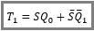
180 State Transition Diagram for Sequence Detector 1/0 Sequence to detect: 0110 Input/output: S/Z Sequence detected AND reset 0 0 State Variables: Q1 Q0 1/1 none 0/0 0/0 state 1 1 0 1 0/0 sequence 011 0/0 0 found 1/0 1 0 1/0 01 Fill in the State Table Present input Present state Present output Next state Flip flop inputs S Q1 Q0 Z Q1* Q0* T1 T2 0 0 0 0 0 1 0 1 0 0 1 0 0 1 0 0 0 1 0 0 0 1 1 1 0 1 1 0 0 1 1 0 1 0 0 0 0 0 0 0 1 0 1 0 1 0 1 1 1 1 0 0 1 1 0 1 1 1 1 1 0 0 1 1
T1 Z ���� �� ���� �� Q1Q0 S 00 01 11 10 0 0 0 1 1 1 0 1 1 0 ����
Fig. 7‐15. Sequence detector design. The state transition diagram, state table, and K‐maps to find the simplified functions for T1 and Z are shown.


