





Welcome to the latest issue of What’s New in Electronics , where we take a closer look at the technologies shaping the future of electrical engineering. From intelligent systems that respond seamlessly to human intent, to the infrastructure challenges underpinning AI’s rapid growth, this edition brings together innovations that highlight both opportunity and complexity across the industry.
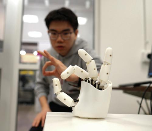
Our lead feature highlights a breakthrough in human–machine interaction: an ultrasound-based wristband capable of translating muscle activity into precise robotic hand control. This innovation underscores the growing sophistication of sensor technologies, where non-invasive, high-resolution measurement techniques are enabling entirely new control paradigms. It also reflects the increasing convergence of AI and sensing — transforming raw biological signals into actionable, real-time outputs.
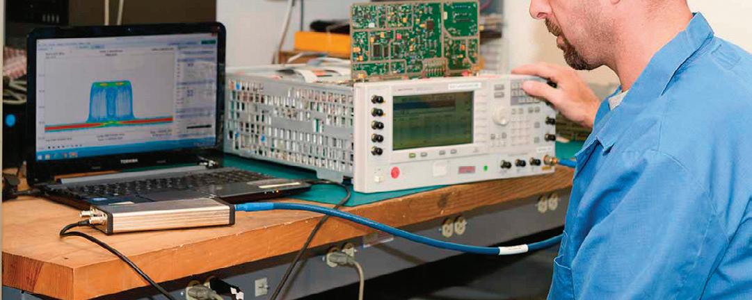
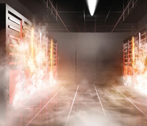
Building on this theme of convergence, the issue also explores thermal constraints in modern data centres. As AI workloads scale, so too does the demand for efficient thermal management. Here, testing and measurement play a critical role, not just in validating performance, but in optimising system reliability and energy efficiency under increasingly complex operating conditions. The challenge is no longer simply about cooling, but about intelligently managing heat as a dynamic system parameter.
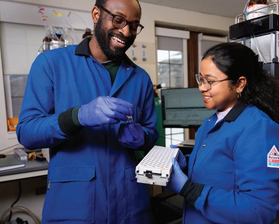
Rounding out the issue is a look at advances in neuromorphic hardware; an area where AI is moving closer to mimicking the structure and efficiency of the human brain. These systems rely heavily on precise sensing, signal processing and validation methodologies, reinforcing the importance of robust measurement frameworks in bringing next-generation architectures to life.
Together, these stories illustrate a common trajectory: the integration of intelligent algorithms with advanced sensing and rigorous measurement, driving innovation across the electrical engineering landscape.
I hope you enjoy this issue and find value in the insights shared. Contributions from across the industry are always welcome. Those with an article idea, technical insight or case study to share are encouraged to get in touch at wnie@wfmedia.com.au, to be part of future issues.
Westwick-Farrow Media
A.B.N. 22 152 305 336
www.wfmedia.com.au
Head Office Unit 5, 6-8 Byfield Street, North Ryde Locked Bag 2226, North Ryde BC NSW 1670 Ph: +61 2 9168 2500
Editor Ashna Mehta wnie@wfmedia.com.au
Publishing Director/MD Janice Williams
Art Director/Production Manager Linda Klobusiak
Art/Production Kate Atkinson
Circulation Alex Dalland circulation@wfmedia.com.au
Copy Control Ashna Mehta copy@wfmedia.com.au
Advertising Sales
Account Manager
Sandra Romanin – 0414 558 464 sromanin@wfmedia.com.au
Asia
Tim Thompson - 0421 623 958 tthompson@wfmedia.com.au
If you have any queries regarding our privacy policy please email privacy@westwick-farrow.com.au
Printed and bound by Dynamite Printing Print Post Approved PP100007394 ISSN No. 0728-3873
All material published in this magazine is published in good faith and every care is taken to accurately relay information provided to us. Readers are advised by the publishers to ensure that all necessary safety devices and precautions are installed and safe working procedures adopted before the use of any equipment found or purchased through the information we provide. Further, all performance criteria was provided by the representative company concerned and any dispute should be referred to them. Information indicating that products are made in Australia or New Zealand is supplied by the source company. Westwick-Farrow Pty Ltd does not quantify the amount of local content or the accuracy of the statement made by the source.
Monash reveals atomic switching in new memory tech
Monash University researchers have captured the exact atomic movements that write data to next-generation memory devices, which could pave the way for smaller, faster and more energyefficient electronics.
Published in Nature Communications, the study is led by Dr Kousuke Ooe, a postdoctoral fellow in the School of Physics and Astronomy at Monash University, in collaboration with Australian Laureate Professor Joanne Etheridge.
Using advanced electron microscopy, the team captured atomicscale movements inside promising memory materials, known as fluorite-type ferroelectrics, that could overcome current limits in how small and efficient memory devices can become.
Everyday technologies, such as smartphones, medical devices, wearable electronics and contactless IC cards used in public transport, store data as billions of digital 1s and 0s.
Flexible films enable next-gen
A soft material developed by researchers at QUT can convert body heat into electricity, opening the door to self-powered wearable devices and more sustainable energy technologies.
Published in Angewandte Chemie International Edition, the research found that the flexible hydrogel captured wasted heat and turned it into usable electrical power with high efficiency.
Team leader Professor Zhi-Gang Chen said the discovery could help power future wearable electronics without relying as heavily on conventional batteries.
In these materials, the physical position of an atom acts like a ‘switch’ — and moving an atom just a fraction of a nanometre is what flips a data bit from a 0 to a 1.
This research shows exactly how that physical movement happens in real time. Until now, scientists couldn’t directly see how this switching actually happened, in fractions of a second.
They discovered that switching doesn’t happen in a single step, but through previously unseen intermediate atomic structures, and that the process can be controlled by changing the material’s composition.
This gives us a completely new level of understanding, not just that switching happens, but exactly how it happens at the atomic scale,” Ooe said.
“What’s exciting is that we can now see pathways to control this behaviour. That opens the door to designing materials that are faster, more stable and far more energy-efficient.”
Etheridge, also from the School of Physics and Astronomy, said. These materials are exciting because they continue to function even at dimensions where conventional materials fail.
The findings provide key design insights for next-generation ferroelectric materials, particularly how different elements influence atomic motion and switching behaviour.
This opens new possibilities for tailoring materials at the atomic level, improving durability and efficiency, and accelerating the development of advanced memory technologies.
“With this gel, we demonstrated how we can turn heat that would otherwise be wasted, such as body heat, into a practical power source. Remarkably, a small 10 mm-square device can generate around 0.46 volts. Although that is a small example, it demonstrates strong potential for real-world applications,” Chen said.
The study was led by QUT researchers Chenyang Zhang, Dr XiaoLei Shi, Wenyi Chen and Dr Qian Liu. Professor Chen said the innovation worked by controlling how charged particles moved through a soft polymer network, allowing the material to efficiently generate electricity from small temperature differences, such as the heat naturally produced by the human body.
Unlike traditional thermoelectric materials, which are often rigid, expensive and difficult to scale, the new hydrogel is soft, flexible, low-cost and suitable for scalable manufacturing, while also delivering excellent performance at room temperature.
The development could enable a new generation of technologies, including battery-free health monitors, smart fabrics and e-textiles, self-powered sensors and Internet of Things devices, and systems that recover wasted heat for useful energy.
This new study adds to a series of research publications in the past few years by the team led by Professor Chen, focusing on the problem of the enormous amounts of energy lost globally as waste heat.
“From powering wearables to reducing emissions, new technologies like this have the potential to transform how energy is captured and used in everyday life,” Chen said.
Jennifer Chu, MIT News
THE NEXT TIME YOU’RE SCROLLING YOUR PHONE, TAKE A MOMENT TO APPRECIATE THE FEAT: THE SEEMINGLY MUNDANE ACT IS POSSIBLE THANKS TO THE COORDINATION OF 34 MUSCLES, 27 JOINTS, AND OVER 100 TENDONS AND LIGAMENTS IN YOUR HAND. INDEED, OUR HANDS ARE THE MOST NIMBLE PARTS OF OUR BODIES. MIMICKING THEIR MANY NUANCED GESTURES HAS BEEN A LONGSTANDING CHALLENGE IN ROBOTICS AND VIRTUAL REALITY.

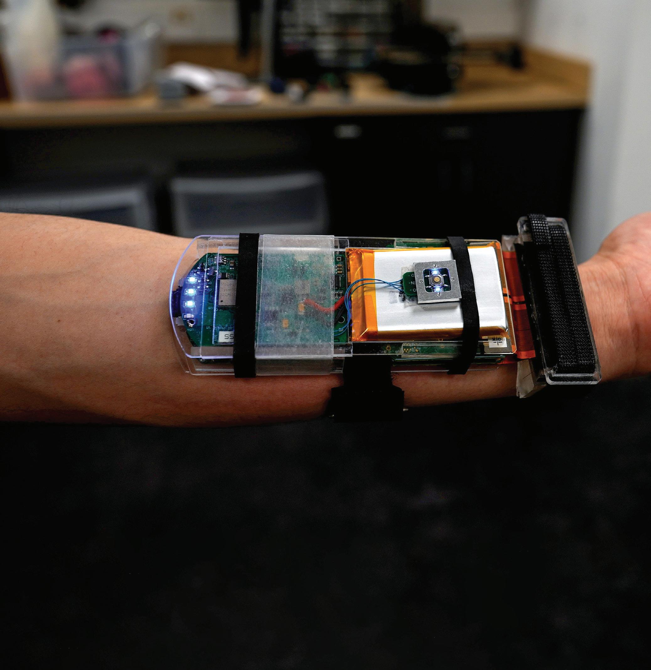
MIT engineers have designed an ultrasound wristband that precisely tracks a wearer’s hand movements in real time. The wristband produces ultrasound images of the wrist’s muscles, tendons and ligaments as the hand moves, and is paired with an artificial intelligence algorithm that continuously translates the images into the corresponding positions of the five fingers and palm.
The researchers can train the wristband to learn a wearer’s hand motions, which the device can communicate in real time to a robot or a virtual environment.
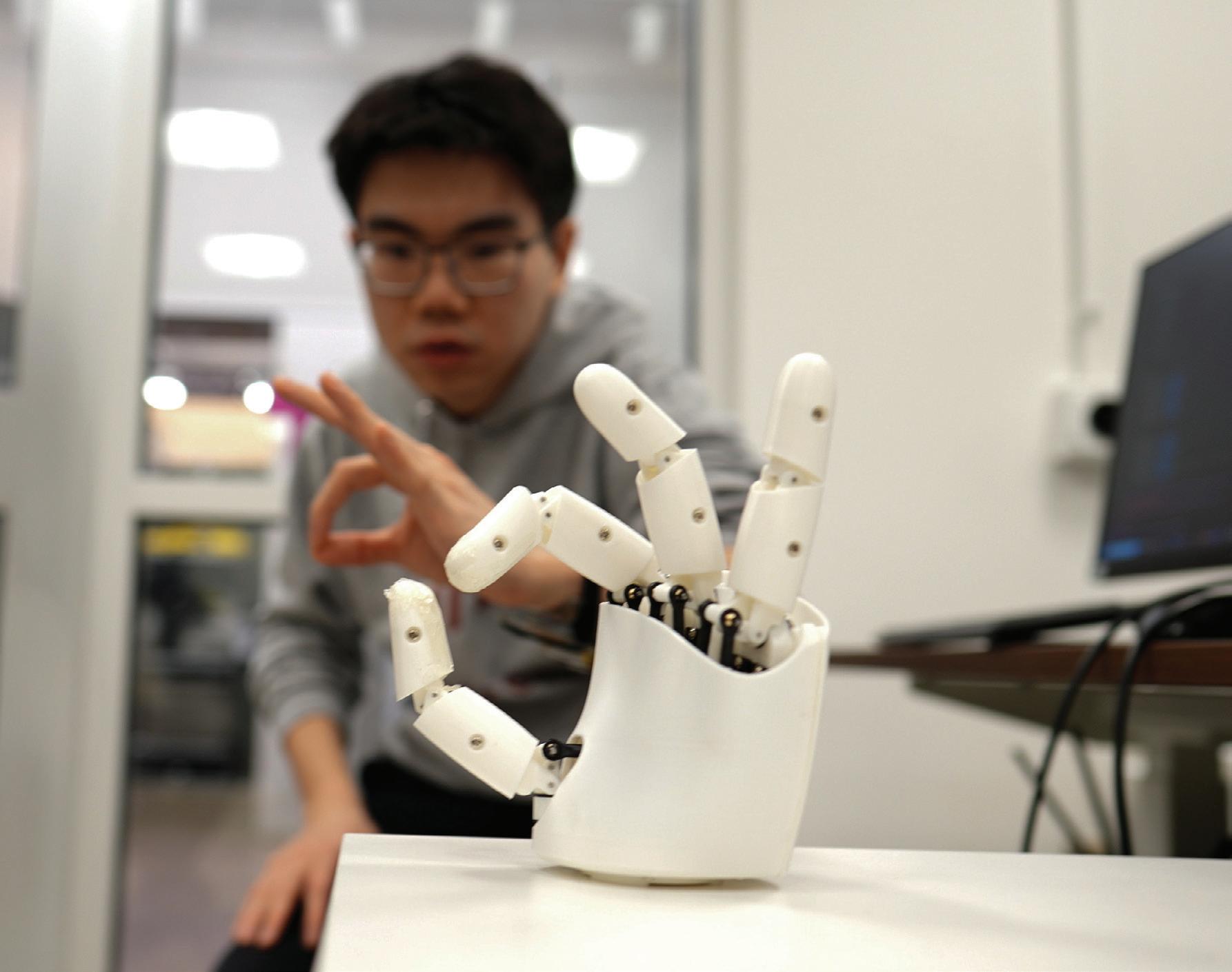
In demonstrations, the team has shown that a person wearing the wristband can wirelessly control a robotic hand. As the person gestures or points, the robot does the same. In a sort of wireless marionette interaction, the wearer can manipulate the robot to play a simple tune on the piano and shoot a small basketball into a desktop hoop. With the same wristband, a wearer can also manipulate objects on a computer screen, for instance pinching their fingers together to enlarge and minimise a virtual object.
The team is using the wristband to gather hand motion data from many more users with different hand sizes, finger shapes and gestures. They envision building a large dataset of hand motions that can be plumbed, for instance, to train humanoid robots in dexterity tasks, such as performing certain surgical procedures. The ultrasound band could also be used to grasp, manipulate and interact with objects in video games, design applications or other virtual settings.
“We think this work has immediate impact in potentially replacing hand-tracking techniques with wearable ultrasound bands in virtual and augmented reality,” said Xuanhe Zhao, the Uncas and Helen Whitaker Professor of Mechanical Engineering at MIT. “It could also provide huge amounts of training data for dexterous humanoid robots.”
Zhao, Gengxi Lu and their colleagues presented the wristband’s new design in a paper appearing in Nature Electronics.
There are currently a number of approaches to capturing and mimicking human hand dexterity in robots. Some approaches use cameras to record a person’s hand movements as they manipulate objects or perform tasks. Others involve having a person wear a glove with sensors, which records the person’s hand movements and transmits the data to a receiving robot. But erecting a complex camera system for different applications is impractical and prone to visual obstacles. And sensor-laden gloves could limit a person’s natural hand motions and sensations.
A third approach uses the electrical signals from muscles in the wrist or forearm that scientists then correlate with specific hand movements. Researchers have made significant advances in this approach; however, these signals are easily affected by noise in the environment. They are also not sensitive enough to distinguish subtle
changes in movements. For instance, they may discern whether a thumb and index finger are pinched together or pulled apart, but not much of the in-between path.
Zhao’s team wondered whether ultrasound imaging might capture more dexterous and continuous hand movements. His group has been developing various forms of ultrasound stickers — miniaturised versions of the transducers used in doctor’s offices that are paired with hydrogel material that can safely stick to skin.
In their new study, the team incorporated the ultrasound sticker design into a wearable wristband to continuously image the muscles and tendons in the wrist.
“The tendons and muscles in your wrist are like strings pulling on puppets, which are your fingers,” Lu said. “So the idea is: each time you take a picture of the state of the strings, you’ll know the state of the hand.”
The team designed a wristband with an ultrasound sticker that is the size of a smartwatch, and added onboard electronics that are about as small as a mobile phone. They attached the wristband to a volunteer’s wrist and confirmed that the device produced clear and continuous images of the wrist as the volunteer moved their fingers in various gestures.
The challenge then was to relate the black and white ultrasound images of the wrist to specific positions of the hand. As it turns out, the fingers and thumb are capable of 22 degrees of freedom, or different ways of extending or angling. The researchers found that they could identify specific regions in their ultrasound images of the wrist that correlate to each of these 22 degrees of freedom. For instance, changes in one region relate to thumb extension, while changes in another region correlate with movements of the index finger.
To establish these connections, a volunteer wearing the wristband would move their hand in various positions while the researchers recorded the gestures with multiple cameras surrounding the volunteer. By matching changes in certain regions of the ultrasound images with hand positions recorded by the cameras, the team could label wrist image regions with the corresponding degree of freedom in the hand. But to do this translation continuously, and in real time, would be an impossible task for humans.
So, the team turned to artificial intelligence. They used an AI algorithm that can be trained to recognise image patterns and correlate them with specific labels and, in this case, the hand’s various degrees of freedom. The researchers trained the algorithm with ultrasound images that they meticulously labelled, annotating the image regions associated with a specific degree of freedom. They tested the algorithm on a new set of ultrasound images and found it correctly predicted the corresponding hand gestures.
Once the researchers successfully paired the AI algorithm with the wristband, they tested the device on more volunteers. For the new study, eight volunteers with different hand and wrist sizes wore the wristband while they formed various hand gestures and grasps, including making the signs for all 26 letters in American Sign Language. They also held objects such as a tennis ball, a plastic bottle, a pair of scissors and a pencil. In each case, the wristband
precisely tracked and predicted the position of the hand.
To demonstrate potential applications, the team developed a simple computer program that they wirelessly paired with the wristband. As a wearer went through the motions of pinching and grasping, the gestures corresponded to zooming in and out on an object on the computer screen, and virtually moving and manipulating it in a smooth and continuous fashion.
The researchers also tested the wristband as a wireless controller of a simple commercial robotic hand. While wearing the wristband, a volunteer went through the motions of playing a keyboard. The robot in turn mimicked the motions in real time to play a simple tune on a piano. The same robot was also able to mimic a person’s finger taps to play a desktop basketball game.
Zhao is planning to further miniaturise the wristband’s hardware, as well as train the AI software on many more gestures and
movements from volunteers with widerranging hand sizes and shapes. Ultimately, the team is building towards a wearable hand tracker that can be worn by anyone, to wirelessly manipulate humanoid robots or virtual objects with high dexterity.
“We believe this is the most advanced way to track dexterous hand motion, through wearable imaging of the wrist,” Zhao said. “We think these wearable ultrasound bands can provide intuitive and versatile controls for virtual reality and robotic hands.”
This is a modified version of a news item published by the Massachusetts Institute of Technology (MIT).
Quantum-inspired wireless tech to boost 6G performance

Researchers at Monash University and The University of Melbourne have developed a quantum-inspired approach to optical wireless communication that could make 6G networks faster, more reliable and energy-efficient.
The research findings, published in IEEE Communications Letters, address a key hurdle for next-generation wireless networks — enabling seamless connections not just between phones and laptops, but also among the chiplets inside computers, smart devices in offices and data centres.
Professor Malin Premaratne, from the Department of Electrical and Computer Systems Engineering at Monash University, is one of the researchers responsible for a method that enables reliable, high-speed connections in crowded spaces, bringing wireless performance closer to “fibre-like” speeds in indoor networks.
Premaratne said that in these environments, conventional wireless signals face serious limitations. “Interference can slow connections, reliability drops in crowded or complex settings, energy consumption and heat restrict performance, and scaling networks requires complex wiring,” Premaratne said.
This research could enable faster and more reliable 6G wireless in homes, offices and public spaces, while powering smarter devices that run cooler and use less energy.
Professor Thas Nirmalathas, from The University of Melbourne, said the team’s innovation uses modular optical phased arrays inspired by principles from quantum physics.
“The research combines quantum-inspired design with optical wireless innovation to tackle key challenges in the design of next-generation ultra broadband wireless systems,” Nirmalathas said.
“Networks built this way can also adapt and grow with future technology demands. Building networks from flexible, reconfigurable blocks allows wireless systems to focus signals precisely where they are needed, reduce interference through polarisation control, improve energy efficiency, and scale easily without redesigning entire networks.”
The Semiconductor Sector Service Bureau (S3B) is leading the development of Australia’s National Semiconductor Roadmap, a 15-year strategic plan designed to strengthen the nation’s semiconductor capability, competitiveness and supply-chain resilience.
Semiconductors power a range of technologies, from smartphones and cars to renewable energy infrastructures. They are also critical to Australia’s defence capabilities and technologies like artificial intelligence and quantum computing.
Globally, semiconductors are considered essential infrastructure and governments are investing heavily to strengthen semiconductor capability and supply chains. Associate Professor and Director of S3B Tara Hamilton said Australia is facing a critical moment to define its long-term direction.
“Australia is heavily dependent on global supply chains. Strengthening semiconductor capability is not just a sector issue. It is fundamental to the resilience and competitiveness of Australia’s most important industries. The Roadmap is the critical next step in supporting and growing the sector, safeguarding our technology industries and enabling broader economic diversification,” Hamilton said.
Scheduled for release later this year, the Roadmap will be an industry-led, evidence-based plan, built on rigorous analysis and strategic insight, designed to provide pathways for policy, investment and capability development.
S3B will carry out a stakeholder engagement phase to ensure the Roadmap reflects the full breadth of Australia’s semiconductor ecosystem.
“Insights gathered from members and partners will inform the starting point for the Roadmap, ensuring the sector’s voice is embedded from the outset. There will be further opportunities for the entire ecosystem including key industry sectors that rely on semiconductors to contribute and help establish a unified national direction,” Hamilton said.
Formal mechanisms, including a strategic advisory group spanning industry, research, academia and government, will also provide guidance throughout the process. Members include former Australian Chief Scientist Professor Cathy Foley and UNSW Chief Scientist and Engineer Professor Hugh Durrant-Whyte.


Lindsey Macdonald, Purdue University
A PURDUE UNIVERSITY ENGINEER HAS USED THE HUMAN BRAIN’S EFFICIENCY AS INSPIRATION TO HELP AUTONOMOUS VEHICLES, SUCH AS DRONES AND ROBOTS, MAKE CRUCIAL, TIME-SENSITIVE DECISIONS WHILE OPERATING IN THE FIELD.
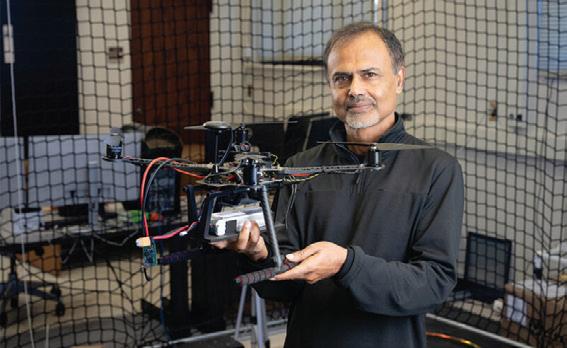
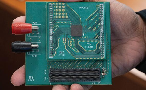
Kaushik Roy, the Edward G. Tiedemann, Jr. Distinguished Professor of Electrical and Computer Engineering in Purdue’s Elmore Family School of Electrical and Computer Engineering, is developing braininspired hardware that enables autonomous devices to efficiently navigate and adapt to their environment.
AI-powered machines have advanced significantly over the past several decades thanks to machine learning, which enables these devices to recognise patterns and
make predictions or decisions. But the algorithms that facilitate this learning require immense amounts of energy to operate due to their intensive calculations and the design of the hardware that runs them.
“Today’s AI devices are designed with separate processing and memory units,” Roy said. “It takes a lot of energy to move the data from the memory to the processing unit and then perform all these complex operations. This is particularly problematic for machines like drones that need to process information
quickly and efficiently to avoid obstacles while completing their assigned tasks.”
To solve this energy problem, Roy and his team are developing a system of sensors, algorithms and hardware that allows autonomous, vision-based vehicles to move from point A to B while avoiding obstacles, optimising energy use and operating independently.
“From the little we understand of the brain, computation and memory are not separated, essentially making it the most efficient processor imaginable,” Roy said. “That’s why we’re taking more direct cues from the brain and co-designing hardware and algorithms that will optimise a variety of AI devices.”
At the heart of this system are algorithms called spiking neural networks (SNNs). All neural networks comprise layers of artificial neurons that activate when presented with information, much like how a biological neuron works within the brain. However, unlike the brain, all the neurons in a traditional neural network activate with every input of information, thereby expending large amounts of energy with every calculation and every decision or action taken by the network.
On the other hand, the individual neurons in SNNs only fire, or ‘spike’, when they receive important information. What is deemed ‘important’ to a particular neuron is based on an assigned membrane potential

— a threshold that determines when a neuron activates. An input or piece of data must reach that threshold for a neuron to spike and produce a reaction. Therefore, each neuron only processes and stores ‘memories’ relevant to their function.
“The membrane potential of each neuron acts as memory, allowing the network to remember the past, much like biological neurons do,” Roy said. “This behaviour turns out to be very useful for sequential and time-based tasks. These are the types of tasks that drones and other autonomous vehicles are performing as they collect information from their environment and use it to make decisions about what to do next.”
While a neural network that fires selectively is a strength in terms of processing power, it introduces a weakness in training. Traditional neural networks learn from their mistakes by relying on backpropagation — a constant flow of information through the network’s layers of neurons that helps figure out where and how mistakes occurred. The selective firing of SNNs produces inconsistent activity and less information. And while the timing of a spike is critical to improving an SNN, the backpropagation in a traditional system is designed to track only where errors occur, not when.
To address these problems, Roy and his team have developed hybrid neural networks that combine strengths of both
traditional neural networks and SNNs. This combination captures timing information effectively while remaining trainable and compact enough for autonomous devices.
Event-based cameras enhance navigation
Two such algorithms, called Spike-FlowNet and Adaptive Safety Margin Algorithm, help special event-based cameras attached to the vehicles more effectively scan and process their environment.
Much like the individual neurons in an SNN, the individual pixels in an event-based camera operate independently, and the camera only records when there’s a movement or change happening in the pixels. This differs from traditional cameras, which record an entire scene — all the pixels at all times.
The cameras mimic how humans interpret visual data through two key aspects of the visual system: rapid eye movements and how the eye focuses. This approach helps event-based cameras process a scene more quickly by prioritising regions of interest over frame-by-frame computation.
“Human visual systems focus sharply on a specific region and use rapid eye movements to scan a scene efficiently,” Roy said. “Our work incorporates these mechanisms into artificial vision systems so they focus their computational resources on the most relevant parts of a scene, like a moving object, rather than processing everything equally.”
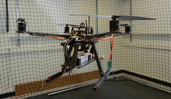
Roy and his team have tested this
technology on a drone, with the vehicle successfully navigating around moving rings in real time.
“Using vision sensors only, the drone can avoid stationary and moving objects and reach its target without collision,” Roy said. “While doing this, it has to determine how objects move in the visual field, estimate depth and then plan a path. These are timedependent operations, where understanding how things change over time is critical.”
Computation and memory converge in specialised hardware
Hardware, the final component of Roy’s system, is currently under development. He aims to harness in-memory computing to eliminate what is termed the von-Neumann bottleneck — the pathway that data must travel between a computer’s central processing unit and memory, often resulting in computational lags.
The hardware in development effectively eliminates that pathway by mapping computational operations and processes directly onto a memory chip.
One device, an electronic synapse that mimics how the brain learns, works by sending an electrical current through a layer of metal that then produces an effect called spin-orbit torque.
Spin-orbit torque works by moving regions of a magnetic layer in different directions depending on the timing and strength of the current. The device learns when the electrical current physically reshapes the magnetic structure, influencing how strongly the current passes in the future.
Devices like the electronic synapse reduce power consumption, increase energy efficiency and, most importantly, operate without internet connections — crucial for autonomous devices out in the field.
While the demonstrations use drones, the same brain-inspired architectures could apply to ground robots, autonomous vehicles, wearables and other embedded AI systems that need real-time perception and decision-making under energy constraints.

Scientists from the University of Edinburgh have developed a new material that could enable electronic devices to work faster and use less energy.
The research findings indicate the material, which was until now thought near-impossible to make, can act as a highly effective semiconductor — a key component of modern electrical devices.
Using the new semiconductor in electronics such as computer processors or medical imaging devices could help them run more efficiently, the team says.
The material — made by combining the chemical elements germanium and tin — can absorb and emit light more effectively than commonly used semiconductors made of silicon.
It works by facilitating the conversion of light into electrical energy, and vice-versa, which is key to the operation of so-called optoelectronic devices.
While previous research had suggested that the germanium–tin alloy could in theory act as an effective semiconductor for converting light to and from electrical energy, producing it had proven very challenging.
This is partly because the elements do not chemically react with each other under normal conditions.
Now, a team led by Edinburgh researchers has created not just a single material, but an entirely new class of semiconductors made of germanium–tin.
The approach involves heating mixtures of germanium and tin to more than 1200°C, while applying pressures of up to 10 gigapascals — around 100 times greater than the pressure at the bottom of the Mariana Trench, the deepest point in the ocean.
The process produces stable germanium–tin alloys at room temperature and pressure that could function as effective semiconductors.
The research has been published in the Journal of the American Chemical Society.
“This work opens up fertile avenues for new materials design through our newly defined inconcert route of creating reactivity and directing recovery of materials with desired crystal structure. This is demonstrated here towards addressing the growing power demand of electronic devices and data centres that need innovative paths to new materials that could boost energy efficiency by using light,” said Dr George Serghiou, School of Engineering.
Researchers at Rochester Institute of Technology (RIT) have developed a new computer chip design approach that allows electronic systems to automatically adapt to real-world conditions, improving how devices manage power in everyday use.
The results show improvements in how chips are designed and how power is managed for always-on electronic systems, from sophisticated biomedical wearables to smart devices such as locks, thermostats and appliances.
The team at RIT’s RF Analog Mixed Signal Laboratory (RAMLab) introduced an adaptive analog design approach for semiconductor chips that allows power delivery circuits to dynamically respond to real-world variability, enabling more reliable sensing and energy-efficient electronic systems. The work addresses key aspects of power management, including how circuits handle changing loads, maintain stable voltage, and suppress noise disturbances that distort or degrade system transmissions.
Their work improves ultralow-power low-dropout, or LDO, regulator design — a key function in power management of computer chips. The approach was tested on a custom chip designed in-house demonstrating energy efficiency during both low power ‘sleep’ modes and active operation.
“Our work is motivated by the need for circuits that can adapt to these changing conditions in real time,” said Teju Das, associate professor in the Electrical and Microelectronic Engineering Department in the Kate Gleason College of Engineering.
An expert in analog, RF and mixed signal integrated circuits, Das described the work done by the team over the past 18 months. The research findings were published in IEEE Transactions on Circuits and Systems.
“At a high level, the circuit we developed continuously monitors its operating environment, such as changes in load, noise and signal conditions, and dynamically adjusts its behaviour to maintain stable and efficient operation,” said Daniel Zeznick, one of the paper’s authors and a teaching assistant with the RAMLab.
Modern electronic systems, especially in areas like wearable health monitors, biosensing systems and Internet of Things sensors, operate under highly variable conditions. However, most power circuits today are designed assuming relatively fixed operating conditions or require external control, which can lead to inefficiencies, instability or degraded performance in real-world use.
“Our work introduces a fully analog, self-adaptive approach in which the circuit continuously adjusts its behaviour based on its operating environment, without requiring external control or discrete events. Rather than optimising for a single operating point, this enables reliable performance across a wide range of conditions,” Das said.
This shift from static or externally controlled operation to continuous, low-overhead adaptation allows for more efficient operation, particularly in energy-constrained systems where even idle power consumption matters. The progression of these concepts highlights the nature of analog and mixed-signal chip research, where developing and validating new ideas in hardware requires sustained effort across multiple stages of design, fabrication and measurement.
This is a modified version of a news item published by Rochester Institute of Technology.
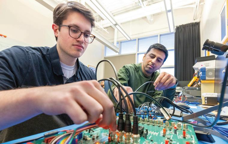
Daniel Zeznick, foreground, and Teju Das, associate professor of microelectronic engineering, test their integrated circuit on a PCB platform built inhouse to assess power and control in integrated circuits.

RESEARCHERS FROM THE EHU-UNIVERSITY OF THE BASQUE COUNTRY HAVE SHOWN THAT BATTERIES MADE FROM BIOMASS MATERIALS STORE SUFFICIENT ENERGY AND CAN ALSO WITHSTAND UP TO 1000 CHARGE AND DISCHARGE CYCLES. THIS DISCOVERY PAVES THE WAY FOR MORE ENVIRONMENTALLY FRIENDLY ALTERNATIVES TO TRADITIONAL BATTERIES.
Over the past few decades, sodium-ion batteries have garnered considerable interest owing to the abundance, low cost and widespread availability of sodium in the Earth’s crust. Sodium-ion batteries are a more cost-effective alternative to lithium-ion batteries (which are widely used, although they have a significant environmental impact) and are less reliant on mineral reserves. However, sodium-ion batteries pose significant challenges, such as low energy density and insufficient charge–discharge cycles.
“Almost all the batteries used in both electric vehicles and smaller devices are lithium-ion batteries. The lithium used in these batteries, as well as other materials needed to manufacture them, such as cobalt, nickel and manganese, are elements on the European Union’s list of critical materials, and efforts need to be made to reduce their use,” said Dr Nekane Nieto, from the EHU’s Materials and Solid-State Group. The group aims to develop sodium-ion batteries using biomass-based materials.
Batteries consist of a cathode (the positive terminal), an anode (the negative
terminal) and an electrolyte, which allows charges to move from one terminal to the other, thereby generating an electric current. The EHU group is conducting research to develop anodes based on carbons obtained from waste biomass collected in the ACBC (Autonomous Community of the Basque Country), in other words, by turning waste into materials that can be used in these batteries. “Our idea is to produce batteries that are as sustainable as possible,” Nieto said.
Button cell batteries
In this study, the team tested various types of biomass, such as coffee grounds, plant stems, shrubbery comprising invasive species, grape seeds and skins, maize cobs, and even compost made from biowaste. “But out of all of them, it was the carbons produced from sunflower seed shells that yielded the best results,” Nieto said. After optimising this anode made from sunflower seed shells, “we paired it with several different cathodes in rechargeable buttoncell batteries, which contain vanadium,
iron and/or titanium in their composition, elements that are not as critical and are used in smaller quantities in these materials”, Nieto said.
With all this in mind, the group carried out a life-cycle analysis to determine which anode/cathode combination offered the best battery performance and the lowest environmental impact. “We achieved some very competitive results compared with the ones described so far. These are rechargeable batteries made from sunflower seed shells that are capable of storing a sufficient amount of energy and withstanding up to 1000 charge and discharge cycles, with the most environmentally friendly cathode chemistry selected for each application,” Nieto said.
Nieto stressed the importance of having manufactured these batteries using biomass materials and components that are not on the list of critical materials. “Although it is true,” she said, “that our batteries are not yet competitive compared with lithium-ion ones, [they] can be used as a complementary system or in small devices”. The group is currently working to develop larger batteries.
Nieto added: “We shouldn’t always focus on batteries that are already on the market. It is always possible to explore a range of approaches and improve sustainability by using waste that is currently not put to any use. It is important to bear in mind that we need to look for alternatives to lithium-ion batteries, and that, going forward, industry may be able to use different types of waste to manufacture batteries, depending on their intended application.”
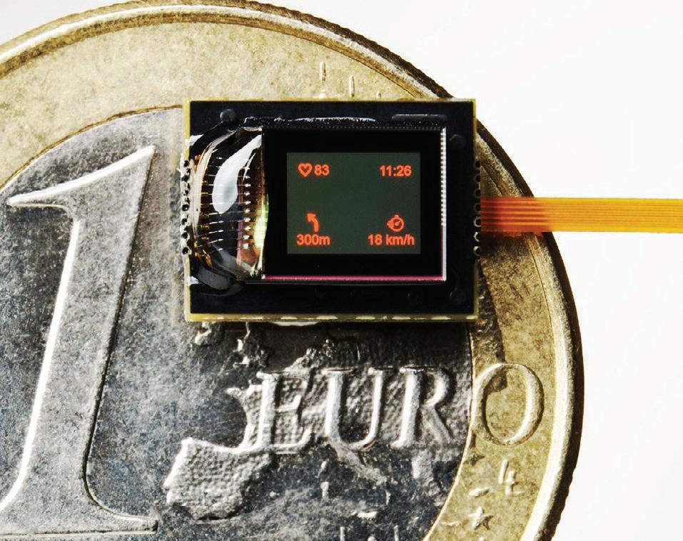
Scientists at the Fraunhofer Institute for Photonic Microsystems (IPMS) have developed a red OLED microdisplay that is both exceptionally bright and highly efficient.
OLED microdisplays are characterised by their compact design, sharp presentations and low energy consumption, making them
ideal for wearable technologies. The latest microdisplay from Fraunhofer IPMS raises the brightness of such systems to a new level. It allows for the display of changing full-graphic symbols, which not only improves precise alignment but also facilitates optical assembly.
Like all other microdisplays from the institute, this new display is based on standard CMOS semiconductor processes, with a silicon backplane serving as the foundation for the OLED technology.
“The new red OLED microdisplay achieves impressive brightness levels of 35,000 cd/m2 while consuming very little power,” said Uwe Vogel, division director of microdisplays and sensors at Fraunhofer IPMS. “Thanks to our ultra-low-power technology, only the necessary pixels are changed for the next image instead of updating the entire image, which saves a tremendous amount of power.”
The high brightness now enables use in data glasses and helmets under daylight conditions. This was achieved through a newly developed OLED stack with highly efficient materials, allowing previously unattainable brightness for red OLEDs. Moreover, the new OLED stack can be transferred to various backplane formats. The scientists at Fraunhofer IPMS are looking forward to customer- and application-specific developments of these new microdisplays, marking another important step in the evolution of display technology.
Australian scientists have created a proof-of-concept quantum battery that can charge, store and discharge energy, opening new possibilities for faster, more efficient energy storage. Fully functioning quantum batteries do not exist yet, but they could transform how energy is stored and used in the future.
The research by CSIRO, Australia’s national science agency, and collaborators RMIT University and the University of Melbourne, has been published in Light: Science & Applications. Dr James Quach, quantum science and technologies science leader at CSIRO, led the team that developed the prototype.
“My ultimate ambition is a future where we can charge electric cars much faster than fuel petrol cars, or charge devices over long distances wirelessly. Our findings confirm a fundamental quantum effect that’s completely counterintuitive: quantum batteries charge faster as they get larger. Today’s batteries don’t function like that,” Quach said.
Quantum batteries leverage unique properties of quantum mechanics such as superposition and entanglement. In contrast, today’s batteries largely rely on chemical reactions.
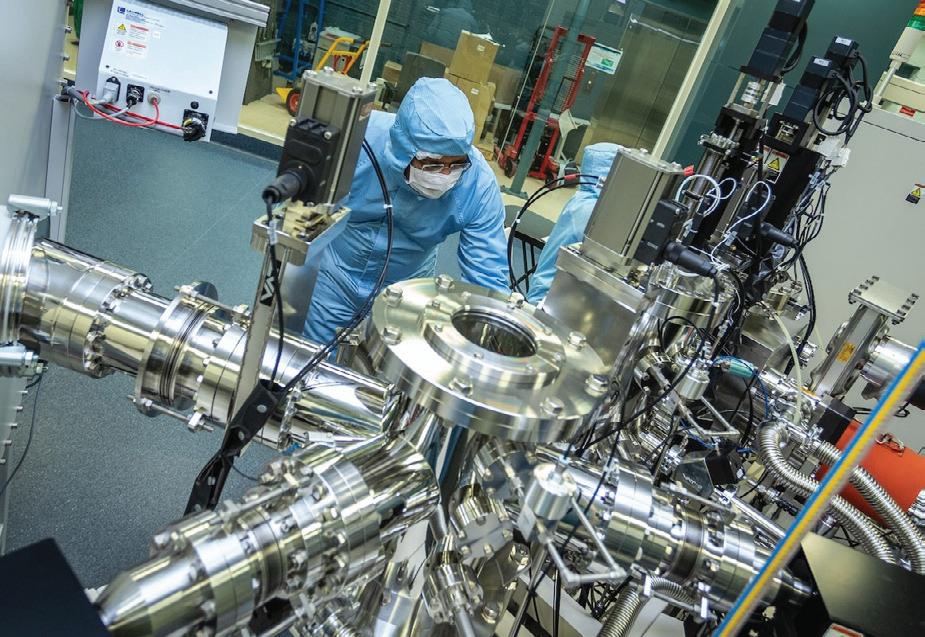
The battery the researchers engineered has a multi-layered organic microcavity and is wirelessly charged with a laser.
The team used advanced spectroscopy techniques to confirm the prototype’s charging behaviour, which showed it retained stored energy for six orders of magnitude longer than it took to charge.
This research proves key predictions about these revolutionary devices and offers a glimpse into a possible future powered by quantum energy storage.
“Our proof-of-concept device showcases rapid, scalable charging and energy storage at room temperature, laying the groundwork for next-gen energy solutions. The next step for quantum batteries right now is extending their energy storage time. If we can overcome that hurdle, we’d be that bit closer to commercially viable quantum batteries,” Quach said.
CSIRO is seeking interest from potential development partners.
A new study has revealed how tiny imperfections and vibrations inside a promising quantum material could be used to control an unusual quantum effect, opening new possibilities for smaller, faster and more efficient energy-harvesting devices.
The international team, led by Professor Dongchen Qi from the QUT School of Chemistry and Physics and Professor Xiao Renshaw Wang from Nanyang Technological University in Singapore, studied the mechanism governing the socalled nonlinear Hall effect (NLHE).
Unlike classical Hall effect, this quantum version allows alternating electrical signals, like those found in wireless or ambient energy sources, to be converted directly into usable direct current without the need for traditional diodes or bulky components.
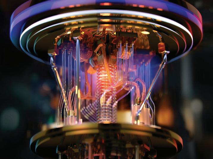
“The NLHE is a sophisticated quantum phenomenon in condensed matter physics where a voltage is generated perpendicular to an applied alternating current, even in the absence of a magnetic field,” Qi said.
“This effect allows us to convert alternating signals straight into direct current, which is what’s needed to power electronic devices. In principle, it means sensors or chips that could operate without batteries, drawing energy from their environment.”
The team studied bismuth telluride, a high-quality topological material known for its unusual electronic properties, and found that the NLHE remains stable up to room temperature.
The direction and strength of the generated voltage was also found to be controlled by temperature.
At low temperatures, tiny imperfections in the material dominated the behaviour. As the material warmed, natural vibrations of the crystal lattice took over, causing the electrical signal to flip direction.
“Once you understand what’s happening inside the material, you can design devices to take advantage of it,” Qi said.
“That’s when quantum effects stop being abstract and start becoming useful — supporting future applications ranging from self-powered sensors and wearable technology to ultra-fast components for next-generation wireless networks.”
The research findings have been published in Newton online.






ARTIFICIAL INTELLIGENCE IS OFTEN FRAMED AS A SOFTWARE BREAKTHROUGH. IN PRACTICE, IT IS ALSO AN ENERGY AND INFRASTRUCTURE CHALLENGE
Asingle AI query can consume roughly 10 times the electricity of a typical internet search, and demand is climbing rapidly.
By 2030, data centres are projected to account for around 3% of global electricity consumption — nearly double their share today and growing far faster than electricity demand from most other sectors.
That level of demand brings with it a practical constraint: heat.
AI infrastructure is becoming denser, more power-hungry and far more thermally intensive than the systems data centres were originally designed to support. Cooling systems that once performed reliably are now approaching their limits.
AI workloads are pushing rack power densities to new extremes.
Where traditional enterprise servers might draw only a few kilowatts per rack,
modern GPU-accelerated systems operate at dramatically higher levels. Today’s fully populated GPU racks draw around 132 kilowatts. The next generation of systems is expected to approach 240 kilowatts per rack, and industry roadmaps are already exploring future densities of one megawatt per rack.
These systems rely on graphics processing units and specialised accelerators that generate intense, concentrated heat loads. Moving enough air through racks at this scale quickly becomes inefficient and difficult to manage.
For decades, air cooling has been the standard approach in data centres. It remains effective at moderate densities, but AI infrastructure is pushing well beyond those thresholds.
Liquid cooling changes the equation. Rather than cooling the surrounding air, direct-to-chip liquid cooling captures heat at the source. Because liquids transfer heat far more efficiently than air, the difference in performance is significant. Direct liquid cooling
can be thousands of times more effective at removing heat from high-density components.
As AI systems scale, this approach is increasingly becoming a necessity rather than an optimisation.
Cooling is typically the second-largest energy consumer in a data centre after the IT equipment itself. Improving cooling efficiency therefore has a direct impact on total power demand.
In many cases, liquid cooling can reduce cooling energy consumption by 30 to 60%. Those gains translate into lower operating costs and lower emissions, particularly in regions where electricity grids still rely heavily on fossil fuels.
Water use is another factor that deserves closer attention.
Traditional cooling towers and evaporative systems can consume large

volumes of water, particularly in warm climates. By contrast, liquid cooling operates as a closed loop at the rack level, meaning the racks themselves do not consume water directly. The overall water footprint then depends largely on how heat is rejected from the facility.
This is where system design becomes critical.
Operating at higher inlet fluid temperatures can significantly reduce both energy consumption and water use. Heat rejection systems also play a role. Air-cooled chillers with economiser modes, for example, rely on cool ambient air to dissipate heat and can dramatically reduce reliance on water-intensive cooling towers.
Component choices matter as well. High-efficiency pumps, durable heat exchangers and coordinated control systems help minimise operational energy while extending equipment lifespan and reducing the embedded carbon associated with manufacturing replacements.
Adopting liquid cooling is an important step, but it is not sufficient on its own. The sustainability of AI infrastructure depends on how facilities are designed and operated. Several factors influence the outcome.
Adopting liquid cooling is an important step, but it is not sufficient on its own. The sustainability of AI infrastructure ultimately depends on how facilities are designed and operated.
Liquid cooling also makes heat reuse far more practical.
Air-cooled facilities typically release low-grade heat that is difficult to repurpose. Liquid-cooled systems, however, produce higher-grade heat streams that can be reused for district heating or nearby industrial processes. While still emerging in many markets, this approach offers a pathway for data centres to contribute energy back into local ecosystems rather than simply rejecting it.
Moving to liquid cooling requires careful planning and coordination.
Historically, IT hardware decisions and facility design have often occurred separately. In the AI era, those processes must happen in parallel. Otherwise organisations risk installing powerful AI hardware that existing infrastructure cannot properly support.
Flexibility is equally important. Hardware generations are evolving quickly, and facilities must be able to accommodate different density scenarios over time. Hybrid environments combining air and liquid cooling are becoming increasingly common, allowing operators to support current workloads while preparing for future systems.
Early collaboration across the technology ecosystem is also critical. Data centre operators, server manufacturers, cooling specialists and infrastructure partners all bring different expertise. Engaging these partners early helps avoid costly redesigns and ensures systems operate as intended once deployed.
Bottom line: efficient cooling is missioncritical for the AI era
AI will reshape industries and economies in the years ahead. But its growth will depend just as much on infrastructure as on algorithms.
Cooling may not attract the same attention as chips or AI models, yet it is quickly becoming one of the defining engineering challenges of the AI era.

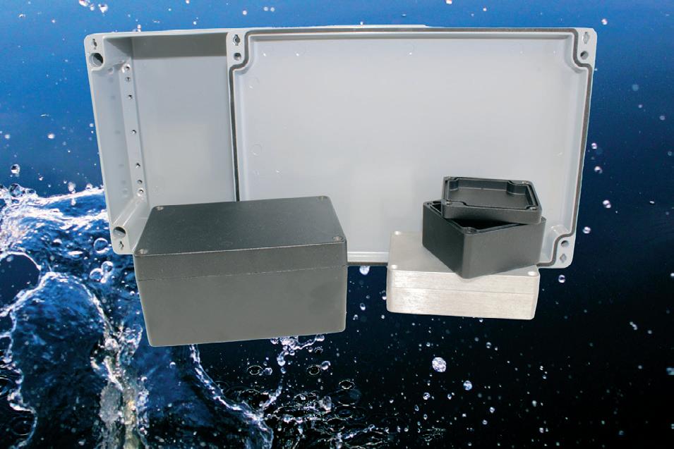
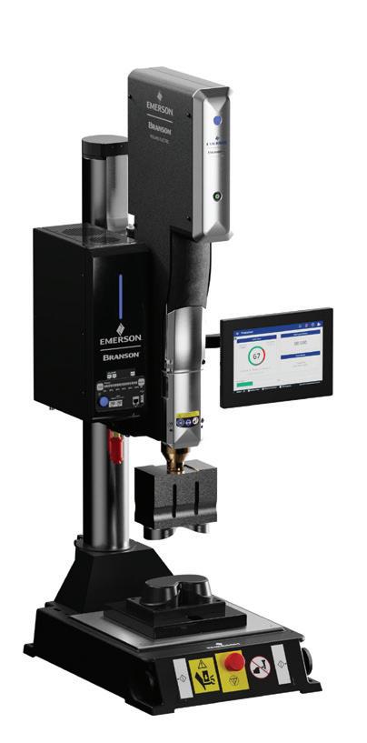
Emerson has launched the new Branson Polaris Ultrasonic Welding Platform, a configurable multi-use welding platform enabling advanced manufacturing engineers to design efficient joining solutions with software and hardware.
The platform offers an adaptable, smart solution with secure connectivity across the factory floor and real-time control capability able to join a range of materials and components, including automotive parts, medical devices, consumer electronics, food packaging, appliances, bioplastics and textiles.
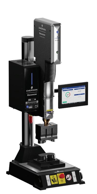
The Polaris platform consists of power supplies and controllers with varying degrees of functionality and software capabilities, as well as a line of actuators that can be selected to meet the needs of any application, regardless of size and complexity.
These technologies can be combined to build a benchtop machine for development, laboratory trials and proof of concept, then scaled up for use in a fully automated production line. Optional features can decrease the system footprint, increase data storage and enhance secure connectivity across enterprise networks.
Allowing for greater visibility and control of machine performance, the platform can connect to higher-level systems such as programmable logic controllers (PLCs) for improved efficiency and precision.
By accessing real-time information, operators can adjust control parameters and recipes in the moment, continuously improving processes and overall equipment effectiveness (OEE). For facilities operating in a regulated environment, the performance data also enables easier validation.
Manufacturing engineers can also select individual components or work with Emerson specialists to create a custom welding system that best suits their needs. Specialists from Emerson can also provide expert technical support throughout the full lifecycle of the welding system.
EMERSON www.emerson.com/au/automation








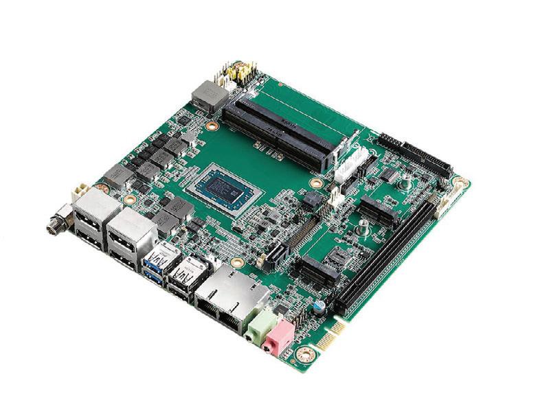
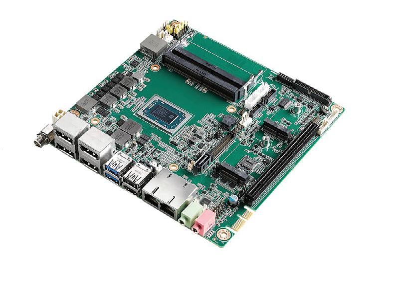
Advantech has expanded its Edge AI portfolio with a new range of embedded computing platforms powered by AMD Ryzen Embedded 8000 Series processors. The line-up includes the SOM-6873 COM Express Compact module, AIMB-2210 MiniITX motherboard and AIR-410 AI inference system, all designed to deliver high-performance AI processing at the edge for industrial and commercial applications.
A key advancement is the integration of neural processing units (NPUs), which, alongside CPU and GPU architectures, enable up to 39 TOPS of AI performance. This enhances inference efficiency while maintaining power optimisation. With support for DDR5 memory and PCIe Gen4, the platforms offer improved responsiveness and scalability for dataintensive workloads.
Each solution is tailored for different deployment needs. The SOM-6873 provides a compact, modular design with up to 96 GB DDR5 memory, rich I/O and consistent thermal performance. The AIMB-2210 balances size and expandability, featuring multiple USB ports, PCIe 4.0 and M.2 slots for storage and AI modules. For more demanding applications, the AIR-410 supports high-end GPU integration and includes a built-in power supply for compute-intensive environments.
Performance gains include up to 1.6x improvement in CPU and GPU capability over previous generations, and up to 1.79x better AI performance in models like YOLOv8, supporting applications such as machine vision, healthcare imaging and smart retail.
Complementing the hardware, Advantech offers software tools including the Edge AI SDK, DeviceOn and iManager for streamlined deployment, remote management and system optimisation. Supporting Windows 11 LTSC and Ubuntu LTSC, these platforms provide flexible, scalable solutions to accelerate AI adoption across multiple industries.
ADVANTECH AUSTRALIA PTY LTD www.advantech.net.au
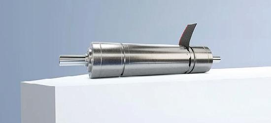
The DualGear drive system from FAULHABER is a compact solution designed for applications in smart logistics where space efficiency and torque transmission are required. The system combines a brushless DC motor with a dual planetary gearhead arrangement, enabling high torque density within a small installation envelope.
The DualGear concept integrates two gear stages into a single housing, allowing loads to be distributed more evenly across the gear train. This design supports longer service life under continuous operation and frequent start–stop cycles, which are common in automated logistics systems such as autonomous mobile robots, conveyor modules and handling units.
The drive system is suited to applications that require precise motion control and consistent performance, even under varying load conditions. Its compact dimensions make it suitable for confined installation spaces, while the modular configuration allows it to be combined with suitable controllers and encoders depending on application requirements.
Typical use cases include material transport systems, automated storage and retrieval solutions, and mobile logistics platforms where efficiency, controllability and mechanical robustness are required. The DualGear drive system is intended to support scalable automation concepts in intralogistics and related industrial environments.
ERNTEC PTY LTD
www.erntec.net
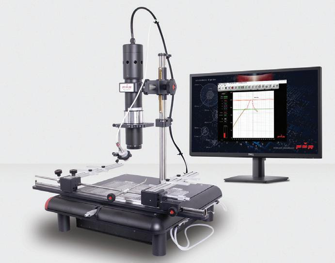
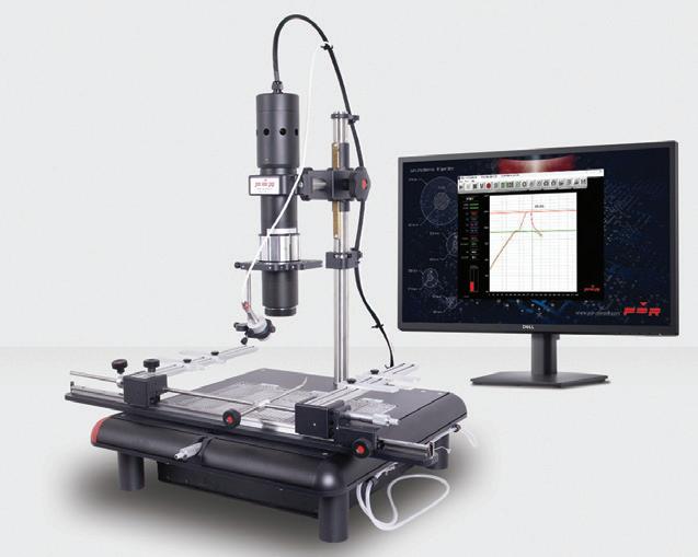
Designed for today’s increasingly complex PCBs, the PDR Focused IR stations are designed to deliver precise, repeatable rework without thermal shock or unnecessary stress to surrounding components.
The rework systems transform complex rework tasks into a stable, intuitive and repeatable process. The result is higher success rates and reduced scrap when working on high-value electronic assemblies.
The rework station’s focused infrared heating targets only the component being reworked, for controlled removal and replacement of BGAs, QFNs, CSPs, LEDs and lead-free devices.
PC-based, closed-loop thermal management also allows users to control both component and board temperatures, delivering repeatable results and protecting sensitive assemblies.
The rework station enables tool-free, gas-free operation with instant thermal response, thereby simplifying setup and creating a cleaner, more efficient rework environment.
From entry-level systems, such as the IR-E1, to advanced semi-automated platforms, the rework station’s modular design enables systems to scale as rework complexity and production demands increase.
Now exclusively represented in Australia and New Zealand by Hawker Richardson, PDR brings leading rework capability to local electronics manufacturers and repair specialists.
HAWKER RICHARDSON www.hawkerrichardson.com.au







According to Xingjie Ni, associate professor of electrical engineering at the Penn State School of Electrical Engineering and Computer Science, the key to addressing this roadblock could lie in computers powered by light instead of circuitry.
Ni and his team have developed a prototype device that can accelerate and reduce the energy cost of AI computation, which they detailed in a paper published in Science Advances. Their system routes light through an ‘infinity mirror’-like loop of tiny
optical elements, encoding data directly into the beams of light and capturing the resulting light patterns with a microscopic camera. AI models powered by this lightprocessing unit run faster and require far less energy than conventional electronic computing systems to complete tasks and perform calculations.
In the following Q&A, Ni discussed optical computing, how this new approach is more efficient than previous optical systems and the impacts this research could have on the future of AI and computing technology.
What is optical computing? How is it different from traditional computing technology?
Traditional computers encode data into binary 1s and 0s and perform operations with electronic circuits, a very flexible and reliable approach, but one that consumes significant energy and generates a lot of heat. Optical computing is a way to process information using light instead of electricity — rather than relying on billions of electronic transistors to do calculations step by step, systems feed light through carefully
Many light signals can pass through the same system simultaneously, allowing optical computers to process large data sets incredibly quickly. Xingjie Ni
How has optical computing been used in AI previously? How does your approach improve its implementation?
Since light can process many signals at once and travel extremely fast, these systems can, in principle, execute tasks like pattern recognition at high speed using little energy. This is why optical computing has been explored as an AI accelerator that performs the ‘heavy math’ at the core of many AI models. In most prior demonstrations, however, light handles only the linear, or straightforward, part of computation, where doubling the input doubles the output, and multiple inputs combine predictably.

designed optical components like lenses or mirrors, encoding calculations and relevant answers directly into these patterns of light.
Optical computing offers key advantages for certain math-heavy tasks because photons, the atomic building blocks of light, don’t interact with each other under normal conditions. This means many light signals can pass through the same system simultaneously, allowing optical computers to process large data sets incredibly quickly. These transformations happen at the speed of light, leading to very low latency, and they can be highly energy-efficient because much of the computation can be performed with minimally powered or even passive optical components.
The decision-making that makes AI powerful is nonlinear in nature — meaning the output isn’t proportional to the input, or that you could input a little bit of information or power and receive a much larger response. This behaviour, which drives the highly complex functions AI models can execute, has previously been done electronically or by using specialised optical materials and high-input power. However, that means these actions require extra conversions between optical and electronic signals — resulting in slower, more complex, power-hungry hardware.
Our approach targets this bottleneck directly. Instead of relying on high optical power and special materials to create the needed non-linear behaviour, we use a compact multi-pass optical loop, like an ‘infinity mirror’ in which the light pattern effectively ‘builds up’ a nonlinear relationship between the input data and the output over repeated passes between the mirrors. The core of our system is built from widely available components — like what’s used in everyday LCD displays and LED lights — rather than exotic materials or high-power lasers. By arranging these familiar elements in a multi-pass loop, we can produce the energy AI needs, while remaining compact and efficient.
According to the paper, your optical computing approach could significantly reduce the size and energy requirements of AI systems. What impacts would this have on industry?
Companies are spending enormous amounts on electricity and cooling as AI usage has grown — in many data centres, the biggest problem facing operations is the energy used and heat generated by the GPUs powering AI models, not just the lack of GPUs. If the most computationheavy parts of AI could be done with a smaller, energy-efficient optical module, it would ease that bottleneck. Companies could offer the same capabilities for less overhead cost, which translates to cheaper, more sustainable AI services for consumers.
Today, many devices still must send data back to a cloud because the local hardware can’t run advanced models without draining the device’s battery or overheating. Shrinking the size and power of AI hardware would push intelligence outward — into cameras, sensors, cars, drones, factory robots and medical devices — so they can respond in real time, keep sensitive data local and rely less on constant connectivity. What’s next for this work?
Going forward, our goal is to turn this proof of concept into an optical computing module that is programmable, robust and ready to deploy. We want to offer developers the flexibility to tune the module’s behaviour for different tasks, rather than relying on whatever non-linearity it naturally produces. We’re working to shrink the setup into a compact unit that can plug into real computing platforms, so the optical part does more of the work end-to-end with minimal electronic overhead, and have plans to scale up to larger, more realistic workloads over time.
Although we don’t see this replacing electronic computing, it could substantially accelerate it. Conventional electronics would handle general control, memory and flexibility, while the compact optical module takes on specific, high-volume computations that drive much of AI’s cost and energy use. If this technology matures into something that can plug into today’s platforms, we could power AI models with smaller, faster and more sustainable hardware.
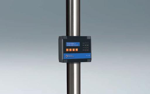
Shipping operators are under increasing pressure to continuously monitor and document vessel emissions to comply with tightening environmental regulations. Continuous emissions monitoring systems (CEMS) are central to this task, measuring pollutant concentrations before and after exhaust gas treatment to verify compliance and assess scrubber performance. However, when these analyser systems fail, operators can be left with critical data gaps. This creates compliance risks, increases administrative workload and may expose operators to penalties. The challenge is amplified at sea, where access to specialist personnel capable of repairing CEMS hardware is often limited.
To address this issue, Endress+Hauser developed a software-based solution that maintains emissions monitoring continuity without relying solely on physical sensors. Its maritime predictive emissions monitoring system (MARpems) applies digital twin technology and machine learning to provide a reliable fallback in the event of analyser downtime, enabling operators to maintain compliance even when instrumentation is unavailable.
The system was developed using data-driven modelling techniques, with machine learning algorithms trained on historical vessel operating data, including engine performance, fuel consumption and scrubber behaviour. These models establish a digital twin of the onboard emissions monitoring system, replicating its functional behaviour under varying operating conditions. By correlating available process variables with expected emissions outputs, the software can estimate pollutant levels and compliance status when direct measurements are not available, reducing reliance on redundant sensing hardware.
Designed as part of Endress+Hauser’s Maritime Suite, MARpems is deployed as an on-premise solution, ensuring that operational and compliance data remains within the ship operator’s IT environment. The software integrates with existing vessel systems and CEMS infrastructure, accessing real-time process data streams. When a sensor or analyser fault is detected, the system automatically transitions to predictive mode, generating validated emissions data based on current operating conditions. The solution has also achieved regulatory acceptance from multiple flag states, including Germany, Malta and Liberia, enabling its use as a compliant alternative during equipment outages.
In operation, MARpems mitigates the immediate risks associated with monitoring system failures while delivering broader operational benefits. Continuous visibility into scrubber and exhaust treatment performance improves transparency and supports more informed decision-making. Predictive insights enable condition-based maintenance strategies, helping to reduce unnecessary servicing and lower overall maintenance costs. The ability to maintain uninterrupted emissions records also simplifies reporting and reduces the administrative burden on crew.
“It’s more than an emergency back-up system — it’s also a strategic tool for greater efficiency and competitiveness in the maritime industry,” said Fabienne Jäckle, team lead for digital product management at Endress+Hauser SICK.
For electronics and instrumentation engineers, the solution reflects a broader shift towards hybrid measurement architectures, where software-defined sensing and data modelling complement traditional hardware. Rather than relying exclusively on physical redundancy, digital twins and machine learning provide an alternative pathway to resilience, particularly in remote environments such as maritime operations.
Endress+Hauser Australia Pty Ltd www.au.endress.com


Hannah Ashton, Oregon State University College of Science
ANYONE SHOPPING FOR A NEW TV IS LIKELY TO NOTICE THE TERM OLED, SHORT FOR ORGANIC LIGHT-EMITTING DIODE. UNLIKE TRADITIONAL INORGANIC SEMICONDUCTORS, OLED DISPLAYS USE THIN, CARBON-BASED ORGANIC SEMICONDUCTOR LAYERS TO EMIT LIGHT, DELIVERING BETTER PICTURE QUALITY, FASTER RESPONSE TIMES AND THINNER DISPLAYS. THAT FLEXIBILITY OPENS THE DOOR TO NEW KINDS OF DEVICES.
The materials that make that flexibility possible are chemically different from silicon and other high-performance inorganic semiconductors, which allows the materials to be printed on a variety of surfaces, bent or stretched, and manufactured at lower temperatures — capabilities impossible with inorganic alternatives.
Physicist Oksana Ostroverkhova studies similar organic semiconductors in her laboratory at Oregon State, exploring how light interacts with these materials and how those interactions can be harnessed to create new optoelectronic and photonic devices. Her work extends beyond semiconductors to organic, carbon-based compounds — including pigments from fungi that can bend, guide light or change colour in response to electricity. She is also advancing spintronics, an emerging approach that transmits information via spin waves rather than electric current.
From televisions to solar cells, the technologies she studies are already part of everyday life, even if most people don’t realise it.
“If we can make them sustainable, low-cost and wearable, that’s an added bonus,” Ostroverkhova said. “Right now, the performance of organic molecules isn’t as good as silicon, and the stability isn’t as high. We want to understand how we can make them perform better and what kinds of tricks we can use to improve them. They’re not going to replace silicon everywhere, but we want to find their niche.”
Focusing on the unique needs of specific products helps narrow down where organic versions can shine.
“For example, disposable sensors. You don’t want to have an expensive silicon sensor telling you whether your milk is still OK to use,” Ostroverkhova said. “We are also thinking about toys and games and other products which shouldn’t need the high performance of silicon.”
Her team is also exploring how organic materials can complement, rather than compete with, traditional versions. “Can we use a carbon-based layer on a silicon solar cell and boost its performance?” she wonders.
The advantages of organic materials could be especially meaningful when it comes to sustainability. Although organic semiconductors don’t produce as many toxic substances during processing, they are still synthesised in laboratories. Ostroverkhova is working with collaborators to explore a natural alternative.
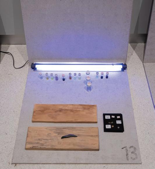
In collaboration with researchers in the colleges of forestry and engineering, her team is investigating pigments like xylindein, a blue-green compound produced by woodeating fungi. Its durability makes it especially compelling, as artists have used it for hundreds of years.
“If something lasts on a church ceiling for more than 500 years and hasn’t degraded from light or heat, I want to know why,” Ostroverkhova said.
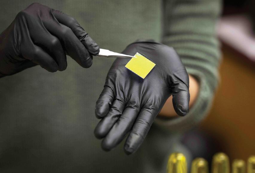
Through their research, the team has discovered that the fungus grows fibrous and highly flexible crystals. Because you can bend them, these crystals can act as waveguides, structures that direct the flow of light.
The pigments can also respond dynamically to electrical signals. “You can apply voltage to some of these pigments and they change colour. So we are thinking of applications where this might be useful,” she said.
In addition to researching what highperformance semiconductors should be made of, Ostroverkhova is also rethinking how they function.
Boosted by a College of Science Research and Innovation Seed grant, she is part of a collaborative research group of physicists, chemists, mathematicians and engineers collaborating on spintronics, an emerging approach to computing that uses magnons, or tiny packets of spin waves, rather than electrical charge to carry information. In conventional
semiconductors, information is processed by moving electrons through a material, generating heat as electrical resistance builds. Spintronics takes a fundamentally different approach: instead of moving charge, it transmits information through waves of electronic spin.
To do that, researchers are relying on a new class of materials known as two-dimensional (2D) magnetic semiconductors, ultrathin materials that can support both electronic behaviour and maintain magnetic order.
Because magnons do not produce resistive heating, they offer a path to faster, more energy-efficient technologies. But to make that possible, scientists first need to understand how these waves move through a material and how to control them. Integration of these 2D magnets with organic molecules could be one of the knobs to tune spin wave propagation.
The group will use the new supercomputer in the Huang Collaborative
Innovation Center to model spin waves with greater accuracy than previously possible.
Looking ahead, Ostroverkhova envisions a world where light-based technologies are integrated into everyday environments in ways that are difficult to imagine today.
“We’re going to have entire walls that function as a display and use touch screens,” she said. “Possibly 3D holographic displays, where you can create a rewritable 3D image.”
While this almost sounds like magic, she emphasises that these advances are rooted in fundamental research, the kind that often goes unnoticed. “People are so used to technology that they don’t think about where all of this is coming from,” Ostroverkhova said. “And it is coming from research labs, doing research in this field.”
This is a modified version of a news item published by Oregon State University College of Science.
Getac has launched its CommandCore rugged drone control station for defence, public safety and utilities in Australia and New Zealand. CommandCore lets customers combine Getac’s rugged hardware with industry-specific accessories, payloads and software based on their individual needs and use cases. The result is a comprehensive UAV/USV/UGV control solution that is fully adaptable and can be tailored to suit a range of challenging environments and operational scenarios, such as those found in the defence, public safety and utilities industries.
At the heart of CommandCore is Getac’s Ground Control Station (GCS), which serves as a centralised, mission-ready hub, designed for realtime data processing, drone control and overall management of operational parameters. Customers can choose between several different Getac devices depending on their GCS needs, including the ZX80 fully rugged Android tablet, UX10 fully rugged Windows tablet, S510 rugged Windows laptop, B360 fully rugged Windows laptop, and X600 fully rugged Windows workstation.
The form factor of the GCS can also be customised for maximum flexibility. Options include a fully integrated design with built-in drone controls and an accessory-type design that lets users separate the Getac device from externally housed drone controls as needed. Additional form factors include an office dock design and a comprehensive suitcase design with dual display for use as part of mobile command and control activity.
CommandCore has been designed to withstand harsh, unpredictable and mission-critical operational environments. Its scalable and configurable system architecture enables seamless customisation, expansion and adaptation to evolving operational requirements across a range of industries.
The drone control solution also integrates smoothly with diverse drone ecosystems, supporting interoperability with third-party technologies and long-term collaborative system evolution. Getac’s GCS is available in both Android and Windows options, while the stable, high-performance computing platform supports real-time, mission-critical operations in demanding situations and environments.
GETAC TECHNOLOGY CORP
www.getac.com

PEROVSKITE SOLAR CELLS ARE WIDELY SEEN AS THE NEXT BIG LEAP IN PHOTOVOLTAICS. THESE DEVICES USE A SPECIAL CLASS OF CRYSTALLINE MATERIALS THAT CONVERT SUNLIGHT INTO ELECTRICITY WITH EXCEPTIONAL EFFICIENCY. HOWEVER, THEIR SENSITIVITY TO TEMPERATURE SWINGS HAS SLOWED THEIR PATH TO OUR ROOFTOPS. RESEARCHERS AT THE TECHNICAL UNIVERSITY OF MUNICH (TUM) AND THE CLUSTER OF EXCELLENCE E-CONVERSION HAVE NOW IDENTIFIED WHY THESE PROMISING MATERIALS LOSE THEIR PERFORMANCE — AND HOW THEY CAN BE STABILISED.
Perovskite solar cells are among the most promising technologies for making solar power cheaper and more efficient. Working with partners from the Karlsruhe Institute of Technology (KIT), DESY (Deutsches Elektronen-Synchroton), and the KTH Royal Institute of Technology in Stockholm, the team uncovered the microscopic mechanisms behind the deterioration of the material through temperature swings and developed a strategy to prevent it. Their approach focuses on stabilising the fragile crystal structure with specially designed molecular ‘anchors’.
To achieve the climate goals of tomorrow, solar cells must endure for decades. While perovskites have reached record-breaking efficiencies in converting solar light into electricity, they face a brutal enemy in nature: extreme temperature changes. Experts refer to this as thermal cycling. In a single day, a solar panel can fluctuate from freezing nights to scorching heat. These real-world conditions, repeated heating and cooling, can trigger an early degradation phase in which perovskite solar cells may lose their relative performance.
“If we want these cells on every roof, we have to ensure they don’t just perform in the lab, but endure the stress of the seasons,” said Professor Peter Müller-Buschbaum,
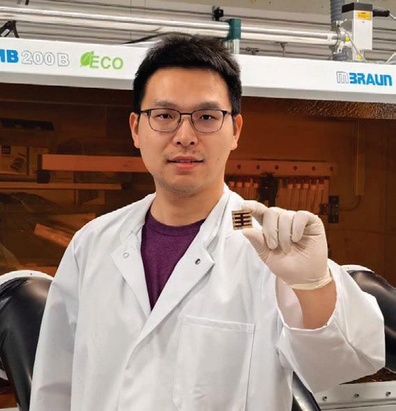
Chair of Functional Materials at TUM School of Natural Sciences. His research team works on this challenge and has identified the microscopic causes of this instability. They developed new design strategies to make the top layer of tandem solar cells more robust, enabling them to withstand real-world conditions. Tandem solar cells are made up of stacked solar cells (two in minimum) and therefore make better use of sunlight.
The ‘burn-in’ phase decoded
In a study published in Nature Communications, lead author Dr Kun Sun from the TUM Chair of Functional Materials
investigated so-called High-Efficiency WideBandgap cells — the upper cells in a tandem solar cell. Using high-resolution X-ray measurements at DESY, the team watched the material ‘breathe’ in real time during rapid temperature changes; the lattice periodically expanded and contracted in response to rapid temperature fluctuations.
The discovery was striking: degradation happens in a massive initial ‘burn-in’ phase, where cells can lose up to 60% of their relative performance. “We revealed that a microscopic tug-of-war triggers this loss. Tensions arise inside the material and its structure changes — this costs power,” Sun said. This finding gives engineers a clear target: if the burn-in can be eliminated, the engineers can unlock long-term stability.
In a second paper published in ACS Energy Letters, the researchers reported how to stabilise the sensitive crystal material. They used special organic molecules that act as spacers, holding the structure together — like a molecular scaffold.
By comparing different spacers, the researchers found a winner: while common spacers led to structural breakdown, the bulkier organic molecule PDMA acted as a superior anchor. The result is a significantly more robust solar cell that remains stable even under the mechanical stress of rapid heating and cooling.
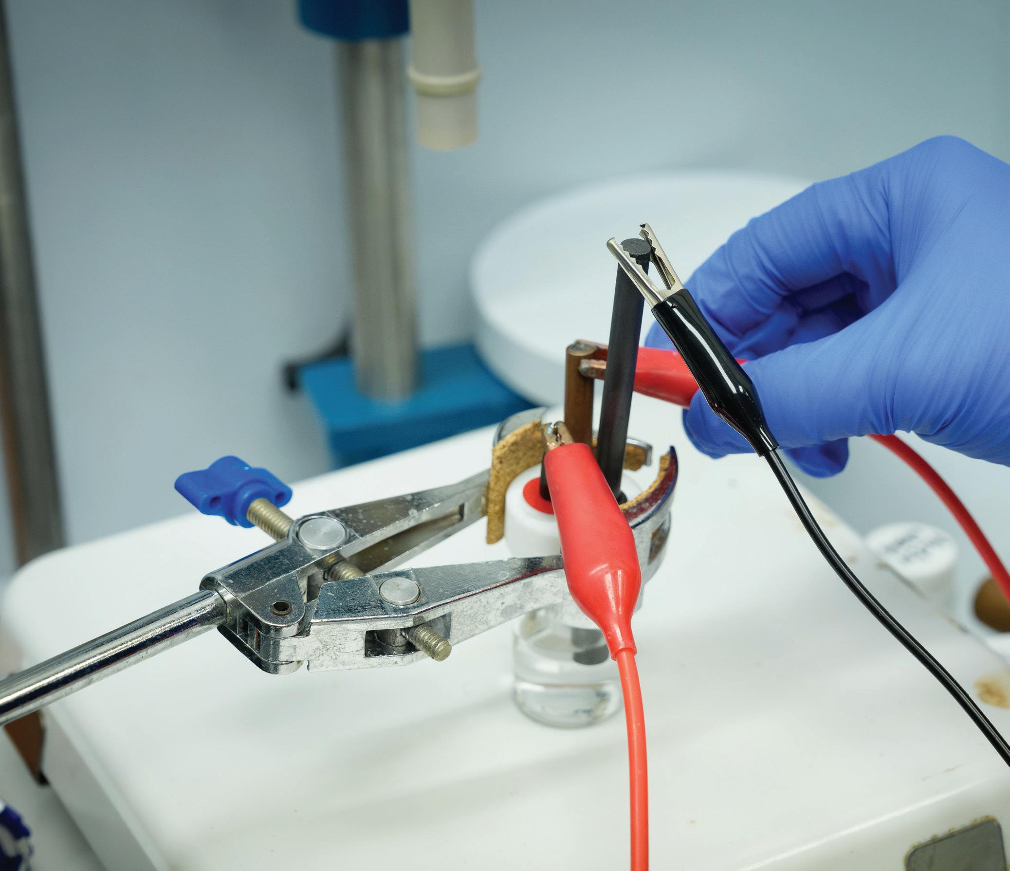
The new method achieved about 94% defluorination and 95% degradation of the PFAS chemical perfluorooctanoic acid (PFOA). Of the 33 PFAS compounds tested, 22 demonstrated degradation amounts exceeding 70%, with some degradation up to 99%.
TALES OF BATTERY BREAKDOWNS AND DEGRADED ELECTROLYTES.
Working with researchers from Northwestern University, the UChicago PME team turned the conditions that unfortunately degrade battery components into a new, powerful technique for intentionally degrading the water pollutants known as per- and polyfluoroalkyl substances, or PFAS.
“If somebody complains, ‘Oh, this compound degrades in this manner and leads to a poorly cycling battery’, we get excited about that,” Amanchukwu said. “Because we can flip it around for PFAS degradation.”
The research findings, published in Nature Chemistry, show remarkable results in breaking down the long-chain PFAS molecule perfluorooctanoic acid (PFOA) into mineralised fluorine without forming short molecular chains that can be even trickier
to remove from water. This new fluorine source can be used to create PFAS-free compounds, turning pollutants into valuable commercial products.
“We achieve about 94% defluorination and 95% degradation. That means we break nearly all the carbon–fluorine bonds in PFAS,” said first author Bidushi Sarkar, a UChicago PME postdoctoral researcher. “We are mainly mineralising and pushing complete breakdown of PFAS instead of just chopping it into shorter fragments.”
As researchers across the globe build ways to destroy the tenacious PFAS molecules through UV light, high temperatures, plasmas, plastic-hungry microbes or other means, this new work sees electrochemistry — the dance between electricity and molecular bonds — joining the fight.
“The reason people love electrochemistry is that it is quite modular,” Amanchukwu said. “I can have a solar panel with batteries, and I can have an electrochemical reactor on site that is small enough to deal with any local waste streams. You don’t need a large plant that operates at high temperatures or high pressures, which are in some of the systems that people are trying to build today.”
Stubborn chemicals, a stubborn question
PFAS are a class of thousands of durable, resilient chemicals used in products including firefighting foams, raincoats, non-stick pans and even the lab coats the team wore during the research. But that durability makes PFAS so difficult to remove from ground, surface or drinking water that they’ve earned the nickname ‘forever chemicals’.
We achieve about 94% defluorination and 95% degradation. That means we break nearly all the carbon–fluorine bonds in PFAS. – Bidushi Sarkar
“All of these properties — fire resistant, water resistant, oil resistant — are because of these strong carbon–fluorine bonds in PFAS,” Sarkar said. “These properties that make PFAS so useful are also what make them so difficult to degrade.”
This PFAS research marks new ground for UChicago PME’s Amanchukwu Lab, which focuses on designing electrolytes for the batteries and electrocatalytic reactors needed to transition the planet off fossil fuels. But after conference presentations and other lectures, Amanchukwu, Sarkar and their team members kept getting questions about a different environmental concern.
“No exaggeration, when I would give talks, I guarantee you a question I would get at the end would be ‘Professor, why are you making more forever chemicals?’” Amanchukwu said.
While the Amanchukwu Lab is pioneering PFAS-free battery electrolytes, many electrolytes contain PFAS, currently in small amounts and not of the type known to cause cancer or other health problems. Rather than dismiss the question, however, the team flipped it: If PFAS-based electrolytes already degrade in batteries, what can scientists learn from that?
The hunt for failure
“The electrochemistry is simply putting electrodes into a solvent,” said Northwestern University Chemistry Professor George Schatz, a co-author of the new work. “If you have these molecules dissolved into solvents, and then you pass current from the electrodes through the solvent, Chibueze and his team developed a scheme where that destroys the PFAS.”
Just zapping water isn’t enough. Breaking down PFAS by oxidising them — removing electrons until the bonds linking the atoms become unstable — is difficult because of fluorine’s chemical properties.
“Fluorine is the most electronegative element, so it really loves electrons,” Amanchukwu said. “This makes oxidising fluorinated compounds hard to do. It is much easier to reduce them.”
Trying to reduce the compounds — adding electrons until the bonds become unstable — kept reducing the surrounding water instead, breaking the water down into hydrogen and oxygen. Studying papers showing PFAS unintentionally degraded in water-free battery electrolytes led to a new plan.
“Our innovation here was working with non-aqueous electrolytes that have high reductive stability, such that when we add a fluorinated compound to it, it’s the fluorinated compound that is reductively degraded,” Amanchukwu said. “That has been the breakthrough that has made this possible.”
Treating copper electrodes with the lithium commonly found in batteries finalised the new procedure. Applying their success with PFOA to other members of the massive ‘forever chemical’ family proved promising for future work. Of the 33 PFAS compounds tested, 22 demonstrated degradation amounts exceeding 70%, with some degradation up to 99%.
“People have done electrochemistry for a long time,” Schatz said. “If it was easy, it would have already been discovered.”
This is a modified version of a news item published by the University of Chicago Pritzker School of Molecular Engineering.
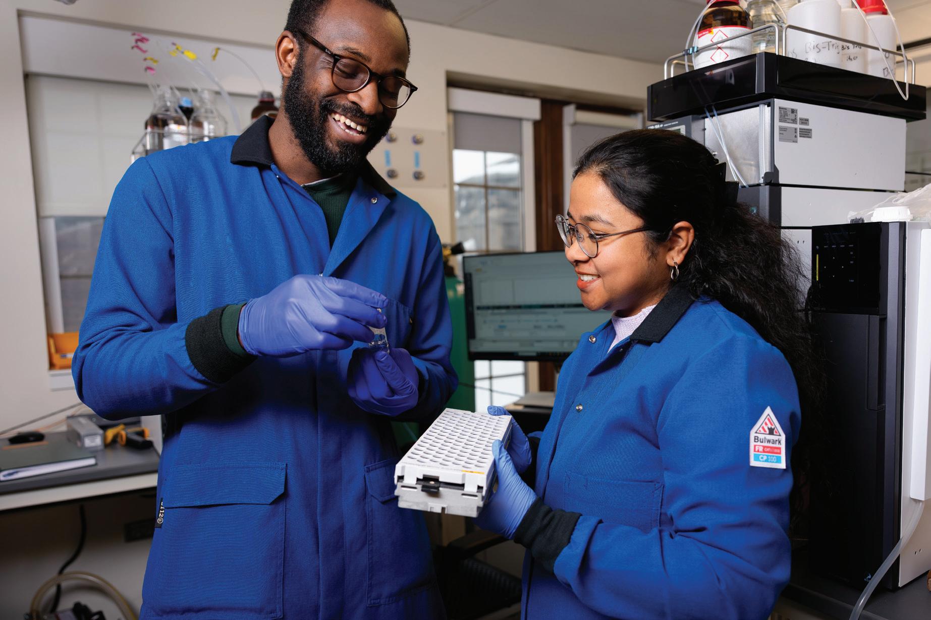

ACCURATELY MEASURING SMALL SHIFTS IN BIOLOGICAL MARKERS, LIKE PROTEINS AND NEUROTRANSMITTERS, OR HARMFUL CHEMICALS IN THE WATER SUPPLY CAN IDENTIFY CRITICAL PROBLEMS BEFORE THEY HAVE A CHANCE TO IMPACT PATIENTS OR THE ENVIRONMENT. WHILE SOME EXISTING SENSORS CAN MONITOR THE MICROSCOPIC MATTER BEHIND THESE ISSUES, THEY OFTEN HAVE LIMITATIONS. A PRIMARY EXAMPLE IS A DEVICE KNOWN AS A FIELD-EFFECT TRANSISTOR — A TINY COMPONENT THAT CONTROLS THE FLOW OF ELECTRICAL CURRENT IN A SYSTEM — THAT STRUGGLES TO REMAIN STABLE WHEN EXPOSED TO LIQUID.
Researchers at Penn State have designed a new type of field-effect transistor that can facilitate responsive and versatile sensing, even in liquid-rich environments like the human body. Sensors built with the team’s transistors were up to 20 times more sensitive to various chemical and biological signals, like hazardous chemicals in water or the levels of dopamine in the brain, than other sensors built with comparable transistor designs. The team published their work in npj 2D Materials and Applications
The technology is based on graphene, a two-dimensional (2D) material that is conductive and highly sensitive to its environment despite being only a few atoms thick. Field-effect transistors used in biosensors have traditionally been constructed with silicon, but are increasingly built with 2D materials like graphene. However, according to Aida Ebrahimi, corresponding author of the paper, when immersed in liquid, these field-effect transistors face signal drift — the sensor’s readings gradually shift over time, even when the inputs measured remain the same, consequently lowering accuracy.
“Aside from signal drift, these devices struggle with electrical leakage and the instability caused by sweeping, a common measurement technique that substantially impacts their reliability over time,” Ebrahimi said. “This makes it difficult to apply these transistors in biointerfaces, like implantable devices, or in any interaction that interfaces with fluid.”
Field-effect transistors essentially work like a tap in a sink, explained Vinay Kammarchedu, an electrical engineering doctoral candidate and first author on the paper. When the tap — or gate, in the language of electronics — is open, the field-effect transistor allows current to flow freely through a system. When the tap or gate closes, the flow stops. However, taking measurements with conventional sensors requires constantly adjusting that tap up and down. According to Kammarchedu, this constant shifting causes instability in the system, leading to inaccurate readings.
“We adjusted the design to have two gates rather than one, allowing us to have independent control over the amount of current flowing through the system,” Kammarchedu said. “Using two gates, we can keep the current running through the system constant, removing a primary cause of signal drift. On top of that, we added a
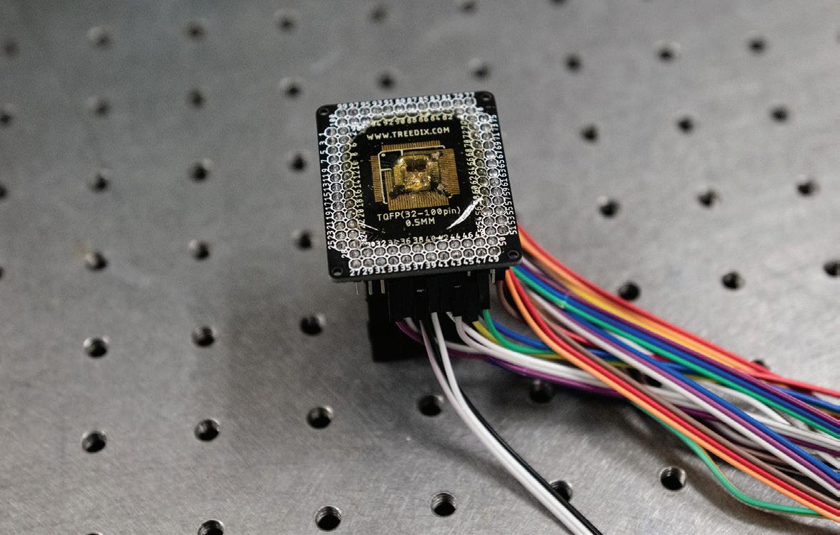
feedback system to one of the gates to more accurately track the impact that molecules have on the sensor’s voltage.”
Kammarchedu explained that the feedback system works by taking advantage of each gate’s different electrical capacity — the top gate has 10 times the capacitance of the bottom gate, meaning it is very sensitive to the environment, while the bottom gate acts as a stiff electronic counterbalance. This relationship between the gates amplifies signals coming through the transistor and substantially increases the sensor’s overall responsiveness.
“If there is a tiny chemical change in the charge at the sensor’s surface, we see it multiplied by 10 in our measurements due to this feedback system,” Kammarchedu said. “This allows us to clearly see very minor changes in chemical readings.”
The team used Penn State’s Nanofabrication Lab to create their transistors, patterning ultra-thin metals, an insulating oxide and a single-atom-thick layer of graphene on top of a base layer made from silicon wafers — polished discs of silicon which serve as a foundational material in chip manufacturing. They then integrated multiple sensors directly into a series of custom circuit boards, which they wired together. To test their design, the team added liquid solutions containing different biological and chemical compounds to the sensors once they were wired into the boards, measuring how well the sensors could track the contents of each sample.
“We can integrate up to 32 sensors and measure each one independently without electrical interference,” Kammarchedu said.
“By stacking arrays of these circuit boards together, we can scale up the number of sensors in a system, all while keeping the sensors themselves very small.”
The team’s sensors demonstrated up to 20 times more sensitivity than other conventional single-gate field-effect transistors and up to 15 times less signal drift. According to Ebrahimi, another major highlight of the sensors is that they can effectively monitor a variety of chemical and biological targets — including neurotransmitters like dopamine and serotonin in the brain; IL-6, a protein agent largely responsible for inflammation; and PFAS, the harmful synthetic chemicals that persist in contaminated water, among other environments.
“Not only are the transistors highly resilient to electrical noise and signal drift, but the engineering improvements we’ve introduced increase their sensitivity substantially,” Ebrahimi said. “This makes the sensing applications extremely broad. They can effectively detect chemicals and biomolecules at low concentrations in healthcare applications, and for agriculture and environmental monitoring.”
The team plans to continue developing the sensing architecture and prepare the technology for commercial use. Currently, they are optimising the sensors to identify volatile organic compounds associated with Parkinson’s disease. By detecting the markers earlier, Ebrahimi said, clinicians could potentially improve early interventions. The researchers are also exploring using different 2D materials in their architecture to possibly improve the sensing abilities of their device.
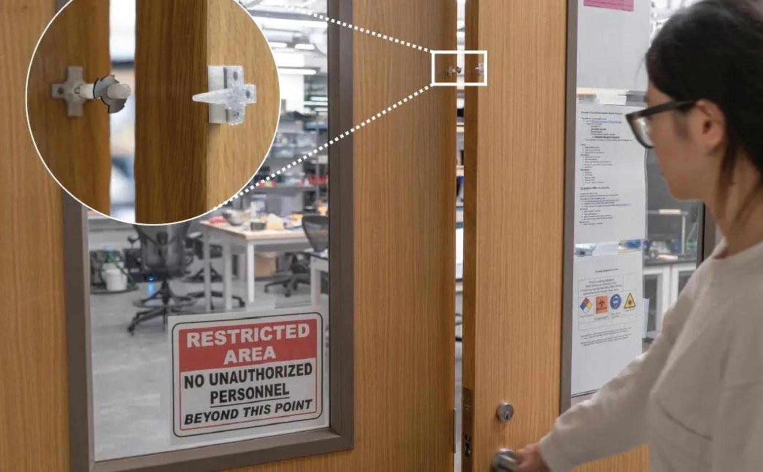
Engineering and computing researchers have created simple metal tags with unique ultrasonic fingerprints to detect door openings and other movements.
Joshua Stewart, Georgia Institute of Technology
MOST SMART HOME DEVICES REQUIRE POWER ONE WAY OR ANOTHER. YOU HAVE TO PLUG THEM IN, RECHARGE THEM OR REPLACE THEIR BATTERIES AT SOME POINT.
Georgia Tech researchers think they have a better way with small metal tags that can signal when a door or drawer is opened, count reps in the gym or even track bathroom use for elderly relatives. Their tags are batteryfree, quiet, inherently private and cost only a few cents each. They’re smaller than a penny.
Like other kinds of smart home sensors, the tags are designed to be mounted on a cabinet or doorframe, for example, using a 3D-printed base. A small tab is attached to the corresponding door or drawer. When it’s opened, the tab strikes the metal disk, triggering a brief ultrasonic pulse imperceptible to human ears but detectable by a wearable device that logs the activity.
The shape of the metal tag — a small disk with a hole in the centre like a flat washer and various cut-outs along the outer edge — determines the frequency of the sound, so each tag can be uniquely identified.
“Those unique fingerprints can be used for smart home sensing, or what we call ‘activity recognition’,” said Yibo Fu, a robotics PhD student who led development of the tags with other engineering and computing researchers.
Fu said the tags could be attached to faucets to help monitor water use or toilet
lids to alert caregivers that an elderly relative might need assistance in the bathroom. Attached to weights in the gym, they could count squats or presses. Users could manually press button versions to trigger a timer or log an activity.
Bolei Deng in the Daniel Guggenheim School of Aerospace Engineering specialises in vibration and waves and how the geometry of an object influences its resonance. He and his team created a modelling and simulation tool to design the metal disks so they would generate specific ultrasonic frequencies when they’re struck.
Their simulations identified nearly 1300 initial designs that would each produce a unique frequency in the ultrasound range. Those frequencies are above 20 kilohertz, which is the upper limit of sounds humans can hear. The team used 15 of the proposed designs in their tests.
“We could select 20 or 50 or 100 designs and it most likely still works,” Deng said. “And with more careful design, I think the total number of available tags can be very, very large — easily thousands — because the ultrasound frequency range is very broad.”
Using ultrasound presents advantages beyond the tags’ silence to human ears.
They’re easy to pick out even in noisy environments. And they don’t travel very far, so only nearby microphones would ‘hear’ the tag. That makes the devices inherently private, Deng said, because other people wouldn’t detect any activity unless they were within a metre or so.
One other way the researchers worked to keep their system simple: they did not use any complicated machine learning algorithms to detect the ultrasound signatures. Instead, they created an algorithm with simple, hardcoded rules. That approach means identifying signals requires little computational and electrical power.
Along with Deng, Fu worked on the tags with School of Interactive Computing researchers Alexander Adams and Josiah Hester.
“This has really been a collaboration between computing and engineering,” Fu said. “There is the physics simulation part, but also there’s the computing we needed to design the algorithm for reading the signals.”
This is a modified version of a news item published by the Georgia Institute of Technology.