20 minute read
The component placement process

The mounting process often utilises pick-and-place systems, which is still the most efficient way to mount components onto boards — but as components get smaller, this process becomes a constant battle to ensure the components are mounted accurately.
Focusing on some of the key challenges during the production of the printed circuit board, including the mounting process, we explore how to overcome some of the pain points, as well as potential difficulties that may occur in the future. Utilising this document to implement a proactive approach may help you to minimise some of these potential problems before they occur.
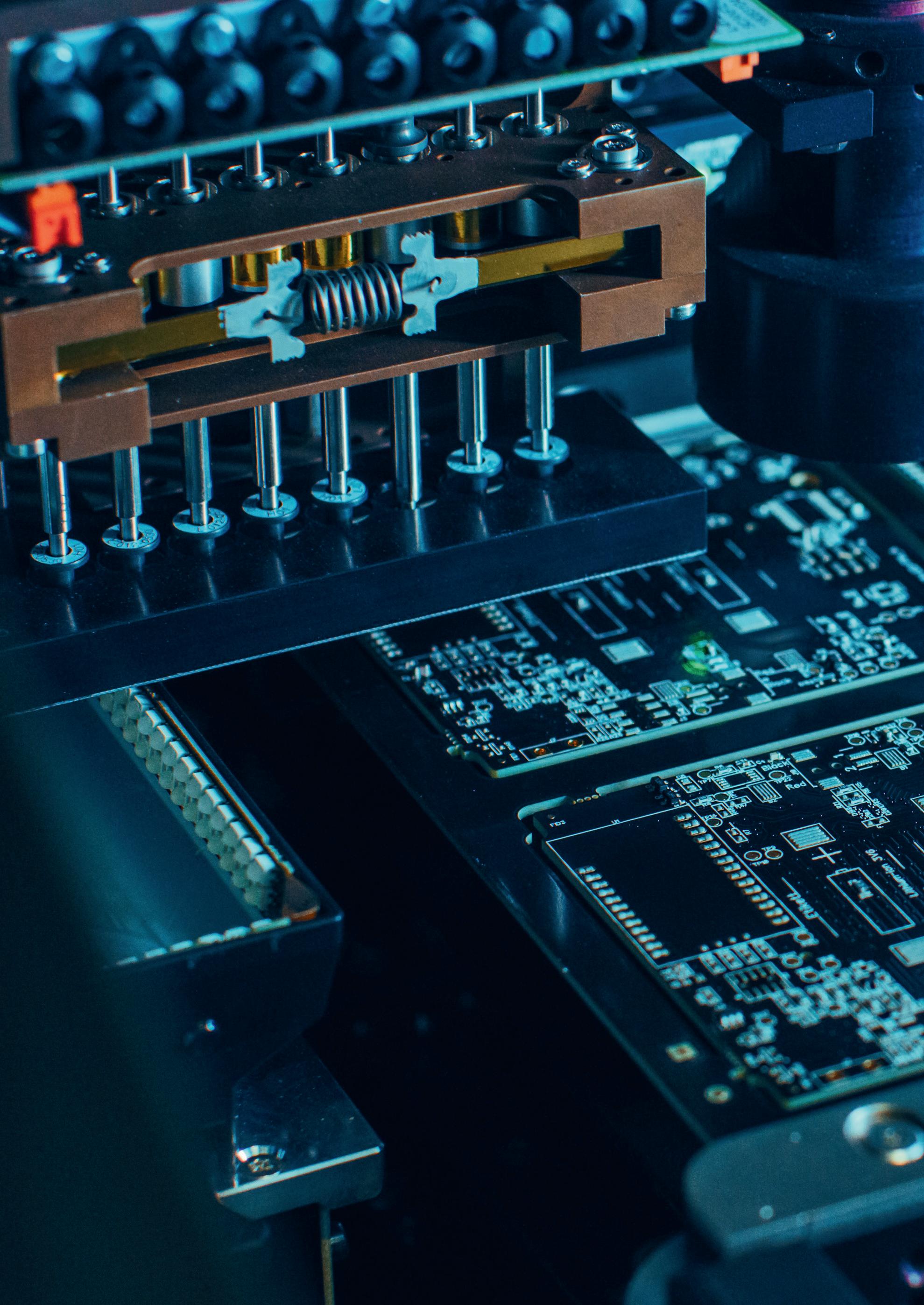
Miniaturisation of holes As we discussed in the article ‘The screen printing process: challenges and considerations 101’, components are constantly decreasing in size, sometimes requiring an aperture size of 0.1 mm. When producing boards requiring apertures of 0.1 mm to accommodate the 0201 chip, it introduces challenges that need to be addressed from the outset such as increasing routine cleaning and inspection. Cleaning: Needless to say, additional requirement to increase these mandatory processes costs valuable time. To minimise wasted production time, some manufacturers have introduced systems that are designed to provide a quickrelease nozzle, using a jig. It can then be replaced with a clean nozzle, while the current part is cleaned in an ultrasonic cleaning system. This process can help to minimise downtime, while ensuring your system is kept clean from debris. Nozzle health check: Checking the health of the nozzle is critical and this can be categorised into two parts — a visual check and a performance check. • Visual check — This can prevent a build-up of debris before it occurs.
Any debris on the nozzle, particularly at the tip, can impact the recognition of the components and potentially lead to mounting failure. Typically, if you
maintain a good clean nozzle, it will ensure you maintain a good recognition rate. A visual check will also ensure the nozzle stays aligned. Any deviation can result in a decrease in pick-up rate, but potentially an increase in mounting failures too. • Performance check — This includes the vacuum functionality and the spring action of the nozzle. Both of these actions are critical in maintaining good pick-up rate and mounting consistency, as well as accuracy. If there are any inhibiting factors preventing the nozzle from performing its full spring action, it can also lead to component breakage.
However, nozzles that are manufactured from ceramics with bespoke ESD coatings improve the stability and durability of the nozzle. This will also help prevent deformation from premature wear, which could lead to the nozzle sticking.
The ESD coating will also ensure that the movement of the nozzle does not create a build-up of electrostatic discharge.
Performing both visual and performance checks are imperative, especially with 0201 components, which require high-precision throughout. This is especially the case during the pick-up process where the components are micro size.
Maintaining high-precision pick-up Maintaining high-precision pick-up requires constant evaluation of several factors including pick-up position and height, as well as the vacuum level and the build-up of static charge from the tape. • Pick-up position — Position of the pickup needs to be accurate, but there are a few aspects that can cause pick-up to become displaced. These include ele
ments such as the accuracy of the tape alignment, nozzle distortion and feeder plate positioning, as well as the actual alignment of the feeding by the feeder. • Pick-up height — Clearly this has to be set up correctly at the start of the process, but there are other variables which can affect the accuracy of the pick-up height including the tolerance of the feeder head and the spring action of the nozzle itself.
Any abnormality in the spring action that inhibits a fluid motion can cause issues with the pick-up height.
Ensuring accuracy and working out any issues with a process of elimination can become tedious and very time-consuming. Some systems have been developed with functionality that enables engineers to teach the machine to maintain both pick-up height and positioning. This is achieved by ‘teaching’ the system to pick up at the centre of
the nozzle every time, by recognising the image of the nozzle tip. It then automatically corrects any deviation off the centre.
Pick-up height can be taught by measuring the pick-up position and the height of the tape by contact tip with the nozzle. Comparison between the current setting can provide a different value. This can be input back into the system for increased accuracy, simultaneously minimising damage to component parts.
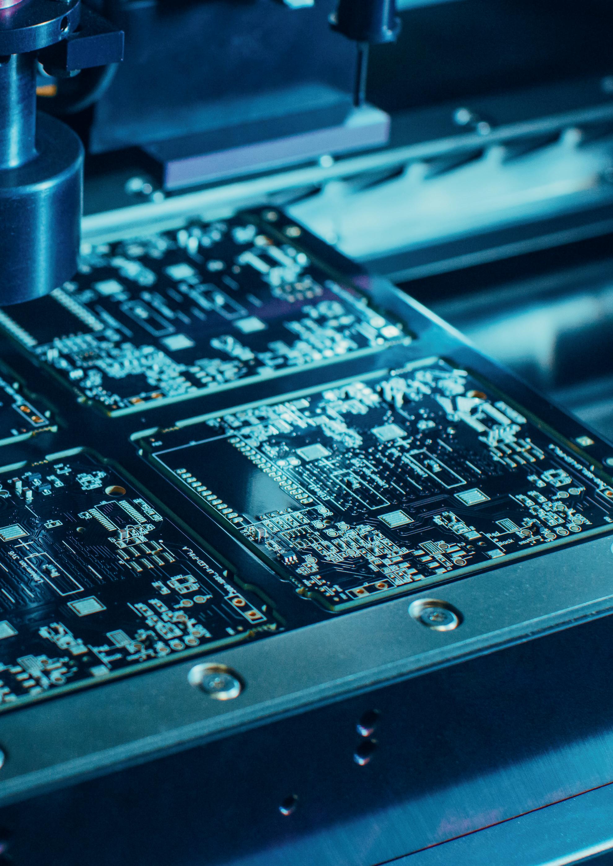
Optimising mounting onto the board Assuming the pick-up height and the pick-up positioning are set correctly, the focus moves onto ensuring the components are mounted correctly onto the board.
One of the main considerations is mask thickness in relation to the component part size. For example, if you are intending to
mount 0201 or 03015 components onto the board, you need to ensure you have set the mask thickness to between 40 and 60 µm.
However, as a component’s size increases it requires a thicker mask, so if the 0201 components are integrated onto the board with larger components (1005), this will require higher levels of mask thickness to account for the variation in the size of the components.
Another solution is to consider utilising solder paste in chip form. Recognising the increasing complexity of board designs, some suppliers now offer the paste in chip form so it can be placed on or next to the pads, where an increase in the amount of solder is required, ie, for the larger components on mixed boards.
Root cause failure analysis (RCFA) Unfortunately, even if you ensure best practice has been implemented and you have done everything you can to ensure production of a good-quality PCB, you could still end up experiencing unexpected faults.
Cameras and vacuum sensors can inform you of issues such as tombstoning, or if the components aren’t released onto the board, but don’t provide any information as to why these issues have occurred.
Utilising a light high-resolution camera with a wide field of view, along with analysis software, could provide rapid analysis feedback, minimising downtime. The software can analyse each image to detect inaccuracies during the pickand-place steps. However, it is essential that the system is configured accurately

EVEN IF YOU ENSURE BEST PRACTICE HAS BEEN IMPLEMENTED AND YOU HAVE
DONE EVERYTHING YOU CAN TO ENSURE PRODUCTION OF A GOOD-QUALITY
PCB, YOU COULD STILL END UP EXPERIENCING UNEXPECTED FAULTS.
and synchronised to firstly capture the image and analyse it at the exact point of picking and placing.
Multi-Accuracy Compensation System (MACS) The MACS system which has been introduced onto some of the Yamaha YS series mounters provides engineers with real-time machine vision. Utilising side-view and upward-looking cameras, the system can identify the centre of the component and, by capturing its position with the centre of the nozzle, it can automatically correct any deviation that occurs in real time.
Utilising the MACS system feature on the Yamaha YS series could reduce positional error from around 30 µm to less than 10.
Checklist Taking everything above into consideration, we have listed the main considerations below, which can be utilised as a checklist. There is no winning formula, because every aspect from the design (including the mixture of component size) to the cleanliness of the nozzle needs to be considered.
Some factors can be counterbalanced with tools and functions on your equipment, such as the ‘teach’ mechanism, helping you to achieve the best results. 1. Invest in an ultrasonic cleaner and a spare nozzle to maintain accuracy and efficiency. 2. Conduct both a visual check and a performance check on the nozzle regularly. 3. Invest in a quality nozzle with an
ESD coating to prevent sticking and electrostatic discharge. 4. Follow the steps to ensure both the pick-up position and the pick-up height are accurately calculated and maintained. 5. Utilise ‘teach’ functionality to ensure accuracy and consistency. 6. Investigate solder paste in chip form.
This can be utilised by your pick-andplace machine, for boards designed with a range of component sizes. 7. Minimise downtime by installing and configuring analysis software to provide feedback on why a failure has occurred. 8. Consider upgrading your system to one of the Yamaha YS series mounters and benefit from MACS system functionality, reducing positional error to less than 10 µm.
New STM32MP1 series @ 800MHz
Boosting Performance, Enhanced Ecosystem

Dual-core Arm® Cortex®-A7 up to 800MHz Arm® Cortex® -M4 core with FPU operating at 209 MHz OpenSTLinux Distribution containing all essential building blocks Continuous investment on Linux and Android to accelerate customer development 3D GPU and HD video decoder for Advanced HMI capability Junction temperature: - 40°C to 125°C 10 years longevity commitment Ideal for smart home gateway, AI, industrial and IoT applications Growing base of partners addressing customers’ challenges
SHORTcircuits
SMART MOLECULES COULD ENABLE COMPUTERS WITH BIGGER MEMORIES
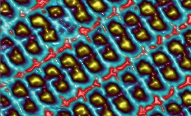
An international team of researchers have discovered a single-molecule ‘switch’, measuring around 5 nm 2 in size, that can act like a transistor and offers the potential to store binary ©stock.adobe.com/au/35microstock that are only one molecule thick, in a process called self-assembly. Ours is the first example that combines all these features in the same molecule.” In laboratory experiments, information — such as the the research team used small 1s and 0s used in classical electric pulses in a scanning computing. Writing in the tunnelling microscope to journal Angewandte Chemie, switch individual molecules the scientists claim that from bright to dark. They molecules like this one could were also able t o read offer information density of and erase the information around 250 terabits per afterwards, at the press of square inch — around 100 An image of the smart molecular switches as seen with a scanning a button. times the storage density of tunnelling microscope. Every bright square is a single switch. During the switching, the current hard drives. electric pulse changes the
In the team’s study, molecules of an organic salt were way the cation and the anion in the organic salt are stacked switched using a small electrical input to appear either bright together, and this stacking causes the molecule to appear either or dark, providing binary information. Crucially, this information bright or dark. Apart from the switching itself, also the spontaneous can be written, read and erased at room temperature and in ordering of the molecules is crucial: through self-assembly, they normal air pressures. These are important characteristics for find their way into a highly ordered structure (a two-dimensional practical application of the molecules in computing storage crystal), without the need for expensive manufacturing tools as devices. Most previous research into molecular electronics is the case in currently used electronics. for similar applications has been conducted in vacuum and at Although the researchers do not expect that the particular very low temperatures. molecules they discovered will be used in real hard drives, the
“There is an entire list of properties that a molecule has study is an important proof of concept that brings us closer to the to possess to be useful as a molecular memory,” said lead brave new world of true molecular electronics. researcher Dr Stijn Mertens, from Lancaster University. “Because chemistry allows us to make molecules with “Apart from being switchable in both directions under ambient sophisticated functions in enormous numbers and with atomic conditions, it has to be stable for a long time in the bright and precision, molecular electronics may have a very bright future,” dark state, and also spontaneously form highly ordered layers Dr Mertens said.
ELECTRONEX 2020 RESCHEDULED TO NOVEMBER
With Electronex –Electronics Design and Assembly Expo set to return to Sydney’s Rosehill Hardens Event Centre later this year, organiser Australasian Exhibitions & Events (AEE) has been closely monitoring the COVID-19 situation and industry associations have been working with federal and state governments in relation to the reopening of business events and exhibitions. Indications are that exhibitions will commence again in the final quarter of this year as restrictions are progressively eased. As a result, a decision has been made to reschedule Electronex from 9–10 September to 10–11 November 2020, to provide sufficient lead time for the event.
While COVID-19 has had a significant impact on the exhibition industry, AEE and the Surface Mount and Circuit Board

Association (SMCBA), the latter of which holds the associated conference, are committed to staging Electronex this year. The event is expected to play a significant role in helping companies generate sales and new business as we come out of this crisis, with the federal government also announcing increased support and stimulus for the manufacturing sector in Australia.
Companies interested in securing a stand at this leading electronics event for the manufacturing and service sector should contact Vee Johnson on 0422 399 818 o r email vee@ auexhibitions.com.au.


SHORTcircuits
EMC TECHNOLOGIES NATA ACCREDITED FOR EN 55035/CISPR 35 The EMC Technologies group of laboratories, located in Melbourne and Sydney, have achieved NATA accreditation for EN 55035 and CISPR 35: Electromagnetic compatibility of multimedia equipment –Immunity requirements. This is believed to make the EMC Technologies group the only NATA accredited labs in Australia for this standard.
Although not mandatory, CISPR 35 has been adopted for use in Australia and New Zealand as AS/NZS CISPR 35 and also published as EN 55035. It is a common EMC emissions standard that is applied to a vast range of ITE and multimedia equipment (MME), including gaming machines, office equipment, modems and many Internet of Things (IoT) devices, and a companion to emission standard CISPR 32 (EN 55032): Electromagnetic compatibility of multimedia equipment –Emission requirements. Both are CE marking EMC standards in the European Union, appearing on the list of harmonised EMC standards used to demonstrate conformity with the EMC Directive 2014/30/EU.
The CISPR 35/EN 55035test standard is intendedto replace CISPR 24 and the EN 55024 and AS/NZS CISPR 24 immunitytests. The approach to monitoring the performance of the device while undertaking testing has also undertaken some changes. The older CISPR 24 test standard on which CISPR 35 is based had more personalised key parameters to monitor based on the type of device such as printers and telephone devices, while CISPR 35 focuses on the primary function or functions of the product under test.
While the CISPR 24 tests have not changed significantly in CISPR 35, there are some new additions — such as spot frequency testing for IEC 61000-4-3 radiated immunity tests — that were not previously required for CISPR 24. This means that even if a product has passed testing for CISPR 24/EN 55024 in the past, there is no guarantee that it will pass CISPR 35/EN 55035. Therefore, it would seem prudent to test the MME to EN 55035 for future products or products that have undertaken modifications.
EN 55035 is currentlylisted on the European Union’s Official Journal (OJ) as a means of demonstrating compliance with the CE Marking EMC Directive, hence to demonstrate the conformity of MME with the immunity requirements for CE marking of electrical products. Showing compliance with this harmonised standard fulfils the first step for CE marking a product for European markets.
EMC Technologies alreadyhas a comprehensive scope fortesting to a range of standards, with the company’s NATAscope of accreditation also including EN 55032. The company provides Australian manufacturers with a route to compliance with the standards and regulations for several global markets.
©stock.adobe.com/au/Sikov

MAGNETOMETRY TO MEASURE THE STATE OF LITHIUM-ION BATTERIES
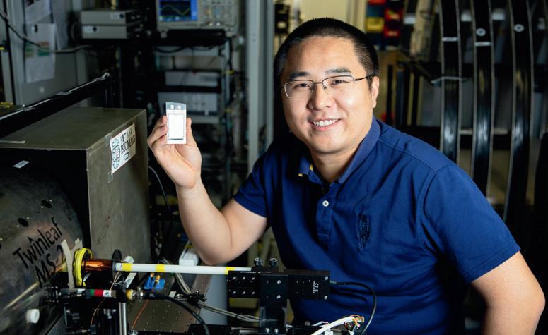
Image ©Arne Wickenbrock
Scientists at Germany’s Johannes Gutenberg University Mainz (JGU) and Helmholtz-Institute Mainz (HIM) have presented a non-contact method for detecting the state of charge and any defects in lithium-ion batteries, using atomic magnetometers to measure the magnetic field around battery cells. Their work has been published in Proceedings of the National Academy of Sciences.
The demand for high-capacity rechargeable batteries is growing, and so is the need for a form of sensitive, accurate diagnostic technology for determining the state of a battery cell. The success of many new developments will depend on whether batteries can be produced that can deliver sufficient capacity and a long, effective life span.
Prof Budker’s group has now achieved a breakthrough by using atomic magnetometers to take measurements — an idea that came about during a teleconference between Prof Budker and his colleague Professor Alexej Jerschow of New York University. They developed a concept and, with close cooperation between the two groups, carried out the related experiments in Mainz.
“Our technique works in essentially the same way as magnetic resonance imaging, but it is much simpler because we use atomic magnetometers,” said DrWickenbrock, referring to optically pumped magnetometers that use atoms in gaseous form as probes for a magnetic field. Prof Budker’s group uses atomic magnetometers for fundamental research in physics.
In the case of battery measurements, the batteries are placed in a background magnetic field. The batteries alter this background magnetic field and the change is measured using atomic magnetometers.


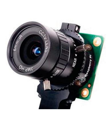
RASPBERRY Pi CAMERA The Raspberry Pi High Quality Camera comes complete with a 12 MP ultradefinition-resolution camera and interchangeable lenses. It is suitable for professional and consumer applications that require high levels of visual fidelity and integration with specialist optics.
The camera can effectively capture still images and video footage. It is compatible with all models of Raspberry Pi boards from the Raspberry Pi 1 Model B onwards and can be used as a desktop camera. It is useful for applications including machine vision, robotics, industrial and agriculture, as well as home and professional security systems that operate in low ambient light conditions. The camera can be programmed to collect data to support facial and number plate recognition and parking space monitoring.
Professional designers will find the camera and interchangeable lens combinations simple to integrate into monitoring and quality control systems while educators, makers and consumers should enjoy the camera’s capability and functionality for Raspberry Pi projects. The camera is designed to extract more information from the lens to create high-quality, content-rich images that could not be achieved by the existing Raspberry Pi Camera Module v2.
The Raspberry Pi High Quality Camera offers a high resolution of 12.3 MP and approximately 50% greater sensitivity than its predecessor for improved low-light performance. It features a circuit board with Sony IMX477 sensor, an FPC cable for connection to a Raspberry Pi computer, a milled aluminium lens mount with integrated tripod mount and focus adjustment ring, and a C- to CS- lens mount adapter. Other lens form factors can be accommodated using third-party lens adapters.
Two interchangeable lenses, a 6 mm wide-angle lens and a 16 mm telephoto lens, can be integrated with the camera’s C- and CS-mount form factors. Users will no longer be limited by fixed lens autofocus cameras, as each interchangeable lens improves the camera’s core functionality as a result of manual focus options including wide and narrow angles and telephoto zoom to identify objects. element14 au.element14.com
REMOTE GPS RECEIVER MODULE ICP DAS’s GPS-721U-MRTU, a remote GPS receiver module, is designed to ensure high sensitivity and low power consumption with an ultrasmall form factor and supports the NMEA 0183 GPS protocol. The embedded GPS module is powered by a MediaTek solution and can provide high performance even in an urban environment or an environment that features dense foliage.
In addition to the ability to acquire GPS data, the module includes a single digital output channel and a single PPS (pulse per second) channel that can be used for precise timekeeping and time measurement. PPS functionality can be combined with an additional external time source in order to synchronise signal operations and provides the full date and time for accurate and precise applications.
Consequently, the product can act as a powerful remote GPS module as well as a general-purpose GPS module with an RS-232 interface. It can also be applied to applications related to automotive navigation, personal positioning and navigation, marine navigation, satellite time correction, etc.
ICP DAS now also provides an option that allows NMEA 0183 format GPS data to be converted to Google Maps format. This feature is available for both the DCON and Modbus protocols from firmware version 2.10 or later. ICP Electronics Australia Pty Ltd www.icp-australia.com.au

SINGLE-BOARD COMPUTER
The MIO-5393 single-board computer (SBC) is powered by a 9th Gen Intel Xeon/Core. With a compact 3.5″ design, the SBC offers good I/O functionality as well as domain-focused features like CAN bus. The small form-factor design functions in broad operating temperature ranges (-40 to +85°C), making it suitable for diverse applications that require high processing speeds, including military defence micro-servers, AOI machines, passenger information systems and outdoor kiosks. The new-generation SBC doubles USB speed by utilising USB 3.2 Gen 2 (10 Gbps). With a built-in Gen9LP graphics engine, the MIO-5393 supports three simultaneous displays with 48-bit LVDS, HDMI (up to 4k @ 30 Hz) and DisplayPort (up to 4k @ 60 Hz). It also supports up to 32 GB/64 GB memory size dual-channel DDR4 2400 MHz and features an M.2 M-Key 2280 slot for supporting NVMe/PCIE Gen3x4 high-speed PCIe SSD storage. The built-in iManager 3.0 integrates power sequence control to improve reliability and enable GPIO, hardware monitoring, smart fan control and watchdog timer functions. Also supported by iManager 3.0 are domain-focused features like high-speed RS-232/422/485 up to 1 Mbps, I²C (100 kb/400 kb/1 Mb) and CANBus. Advantech Australia Pty Ltd www.advantech.net.au

THREE-PHASE BUILT-IN FILTER WITH NEUTRAL LINE SCHURTER’s FMAD CP is a single-stage filter family for three-phase systems with a neutral line. Due to their compact dimensions and high performance, the filters are suited to the tight space conditions in today’s machine and equipment construction. Their extended temperature range means they can also be used in critical applications. The filter family is suitable for devices with high EMC loads at low or medium power. Typical applications include converters for photovoltaics, battery storage or charging stations for electric vehicles. The powerful compact filters are also useful for modern frequency inverters for motor control.
The standard versions can be used over a temperature range of -40 to +100°C. The filters are designed for currents from 3 to 20 A at an ambient temperature of 50°C. They have ENEC and cURus approval and are recommended for applications up to max 520 VAC. Versions with different leakage currents are available for various applications, including industry (≤3 mA), standard (≤0.5 mA) and medical technology (≤5 µA).
Although the filter family is already equipped with high-quality components, an even stronger filter effect may be required for particularly demanding applications. This is where the ‘High Performance’ version comes into play. Due to compact chokes with particularly high inductance and a larger X capacitor, both symmetrical and asymmetrical interference can be suppressed even more effectively.
The filter series has 6.3 x 0.8 mm plug-in connections for quick and easy wiring. Due to a metal flange, a good earth connection is ensured when screwed to the chassis. The series is a suitable replacement for the SCHURTER FMW4-65, offering the same if not higher performance at lower weight. SCHURTER (S) PTE LTD www.schurter.sg