
6 minute read
Low-resourced communities benefit from 3D-printed electronic systems

Suzanne Smith Trudi Joubert
Imagine that a smart and interconnected sensor system can be formed digitally in an economical and environmentally friendly way. Now imagine that it can be done in South Africa, near low-resourced communities who need these products the most. One need not only imagine – the local design and manufacture of smart sensors and wireless sensor networks are precisely the overarching vision of the Integrated Microelectronic Sensor System Research Programme of the Carl and Emily Fuchs Institute for Microelectronics (CEFIM) in the Department of Electrical, Electronic and Computer Engineering.
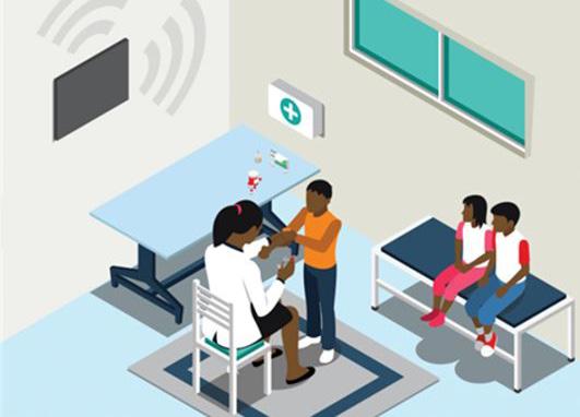
In the midst of the COVID-19 pandemic, with many people working from home during the nationwide lockdown, there is much discussion about the efficiency of combining two important mitigation measures to curb the uncontrolled spread of the disease. These measures are extensive testing and case tracking, which includes contact tracing.
The work of the CEFIM research group envisages appreciable contributions in this context, including the following:
The availability of a low-cost platform for smart rapid diagnostic devices that can be produced locally The interconnection of tests to provide data that initiates case tracking and may simplify contact tracing
The multiplexed microsensor platform that is under development integrates into low-cost printed microsensor systems using printed electronics and integrated sensor micromanufacturing, pushing the boundaries of current solutions. Such a platform can impact not only on point-of-care health diagnostic tools, but also environmental point-of-need monitoring devices. Environmental monitoring, including water quality, is critical to the scientific understanding of global change, and such devices and technologies can assist with responding to these changes.
This multidisciplinary research programme aims to position CEFIM towards innovation relevant to the sustainable development of local communities, while maintaining global relevance and excellence. Historically, CEFIM has specialised in the design of novel integrated microelectronic circuits. Its consistent “more than Moore” 1 approach means that it is focused on improving the functionality of microelectronics through the design of innovative and novel devices and structures, rather than merely the brute force implementation of technology.
The recent inclusion of additive manufacturing in CEFIM’s work aims to be less wasteful of material resources than traditional subtractive manufacturing, while research is ongoing to use manufacturing materials that have a reduced environmental footprint, contributing to a number of the United Nations’ Sustainable Development Goals (SDGs).
Process modelling, analytics and design are important to facilitate technology transfer in this context, in alignment with the global trends of the Fourth Industrial Revolution, machine learning and big data. These design methodologies and modern micromanufacturing technologies are currently being harnessed to realise novel solutions in optical, physical, gas and electrochemical sensor systems.
Important engineering aspects for the platform that are currently being developed are sensor signal transduction and readout, analogue and digital signal processing, algorithmic result extraction, visual or audible results display, data communication and networking, as well as energy harvesting and storage.
Device integration strategies that best exploit modern additive manufacturing technologies are used. Printed functionality enables different functional components to be printed directly onto a variety of substrates, including low-cost options such as adhesive labels, paper and cardboard. By printing onto flexible substrates, system integration into customisable form factors is a possibility. Key processes include planar printed electronics (inkjet, screen and aerosol jet printing) and 3D printing (filament extrusion and stereolithography).

CEFIM’s work considers novel materials for custom-printed sensors. The envisaged solution is illustrated below, showing a flexible, thin device with different building blocks that would be required for an automated, intelligent device to be realised.
Envisaged printed functionality solution and various on-board components for point-of-need applications in health, water, wireless communication and climate sciences. Reproduced with permission from The Royal Society of Chemistry.
Functional blocks such as sensing, electronics, data processing, connectivity, and readout and display are all components that are currently being explored. These building blocks are important in the development of point-of-need solutions, where ideally, low-cost, automated and disposable devices would be needed. This is particularly crucial in resource-limited settings, including clinics and rural villages, where infrastructure is limited. In recent years, there has been a drive to develop low-cost and innovative point-of-need diagnostics to reach resource-limited populations, where the burden of disease is greatest and resources are the least. South African research affords the opportunity to understand first-hand the challenges faced in these settings, and the potential to make a difference where it matters most.
CEFIM’s work focuses on novel electronic components and circuits, with the goal of developing customintegrated circuits and printed electronic devices. Various printed electronic components can be produced by printing single or multiple layers of conductive, resistive, insulating and semi-conductive layers. These include resistors, capacitors, inductors, and even light-emitting structures and transistors. Hybrid printed electronics currently provide feasible implementations, utilising off-the-shelf components and customdesigned, integrated circuits. These are then integrated with printed tracks and other printed circuit components to realise flexible solutions on various substrates. Several printed electronic components, circuits and subsystems have been developed utilising different materials with inkjet and screen-printing processes.
THE MULTIPLEXED MICROSENSOR PLATFORM INTEGRATES INTO LOW-COST PRINTED MICROSENSOR SYSTEMS USING PRINTED ELECTRONICS AND INTEGRATED SENSOR MICROMANUFACTURING, PUSHING THE BOUNDARIES OF CURRENT SOLUTIONS.
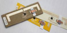
Examples of additively manufactured electronic components and circuits:
READOUT PRINTED HYBRID CIRCUITS
EXAMPLE OF APPLICATION
An example of a solution for health applications involves a low-cost, automated wireless reader device, using cardboard packaging to house printed functionality components. This provides a maintenance-free device that can be deployed in clinics, used several times, and then disposed of. The device provides automated result readouts from diagnostic tests, and communicates the results wirelessly to a central database. The device is low in cost, with the long-term goal of being environmentally friendly and able to be mass produced, using existing and modified industry processes for printing and packaging.
Credit: Trudi Joubert, Suzanne Smith and Petroné Bezuidenhout
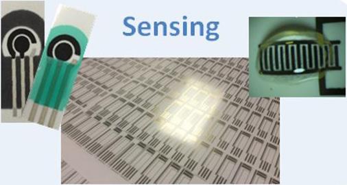
SENSING
WIRELESS COMMUNICATION
Credit: The Royal Society of Chemistry
The specific applications that are currently being explored through various research collaborations include the following:
Medical diagnostic sensor devices Environmental and climate monitoring, for example of water and quality Veterinary diagnostic sensors and remote sampling devices Sensors for agriculture, farming and conservation Energy-harvesting devices to power the additively manufactured devices The aspiration is to facilitate lowcost and low-volume production technologies that will enhance scientific research and support local manufacturing infrastructure, extending to small-scale industrial enterprises. For the upscaling of additively manufactured devices, it will be crucial to work with local companies to pave the way for production and the deployment of intelligent printed devices across Africa. Collaborations have already been established with companies to assist with printing and packaging, as well as the pick-and-place of electronic components onto flexible substrates. Discussions with local companies in areas of wireless communication and printed touch pads and circuitry have also been fruitful. The goal is to maintain and strengthen these networks with industry to establish a pipeline for the development and production of additively manufactured electronic devices and solutions for the future. This work has the potential to make a globally relevant and unique impact in Africa, and by establishing the infrastructure, equipment and expertise required to develop these solutions in South Africa, unique local solutions can be developed for local challenges.
