1 minute read
My workspace


2
3 1
3
5
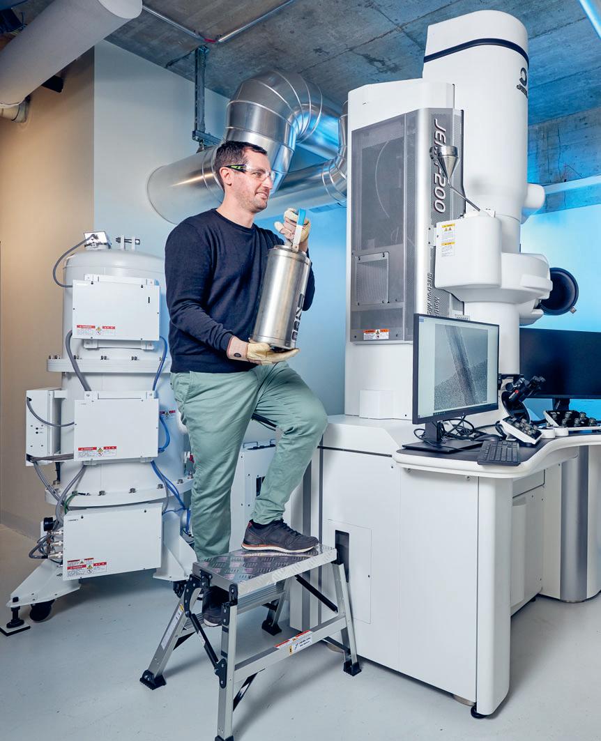
Ice-cold electrons.
A new high-tech microscope recently took up residence at the Nano Imaging Lab of the Swiss Nanoscience Institute. Known as a scanning transmission electron microscope (STEM), the instrument allows researchers to study samples such as new materials with superconducting properties. A highly focused electron beam strikes the material, passes through it, and bounces off atomic nuclei or is defl ected by atomic shells in the process. The resulting pattern of scattered electrons produces an image of the material in which it is possible to distinguish individual atoms.
Markus Dürrenberger (right) has been head of the Nano Imaging Lab for many years and is retiring in summer 2023.
Marcus Wyss (left) is taking over as the new head of the team.
Photo: Oliver Hochstrasser 1 With the new microscope, users can choose between two imaging modes: aiming the beam at the whole sample or focusing it and scanning the sample point by point, which takes signifi cantly longer but produces a much clearer image. The resulting X-rays even provide information about the elements present at various points in the material. 2 The voltage source produces a voltage of 200 kilovolts, which is applied to an electron source (known as a fi eld emission gun) at the top end of the microscope. This voltage draws the electrons out of a fi ne microcrystalline needle tip and accelerates them. 3 The area around the specimen is cooled using liquid nitrogen, which the staff of the Nano Imaging Lab top up at regular intervals using a special container and a funnel. 4 On a special mounting, the prepared sample is introduced via the open chamber door, which must be closed before the vacuum can be built up. A vacuum is needed because air would defl ect the electron beam and disrupt the image. 5 High-resolution images of this kind allow researchers to examine, among other things, the results of newly developed methods for the manufacturing of nanowires for quantum computers.


